EP0421240B1 - Flüssigkristallanzeige - Google Patents
Flüssigkristallanzeige Download PDFInfo
- Publication number
- EP0421240B1 EP0421240B1 EP90118391A EP90118391A EP0421240B1 EP 0421240 B1 EP0421240 B1 EP 0421240B1 EP 90118391 A EP90118391 A EP 90118391A EP 90118391 A EP90118391 A EP 90118391A EP 0421240 B1 EP0421240 B1 EP 0421240B1
- Authority
- EP
- European Patent Office
- Prior art keywords
- liquid crystal
- display element
- crystal display
- liquid
- composite film
- Prior art date
- Legal status (The legal status is an assumption and is not a legal conclusion. Google has not performed a legal analysis and makes no representation as to the accuracy of the status listed.)
- Expired - Lifetime
Links
- 239000004973 liquid crystal related substance Substances 0.000 title claims description 94
- 239000002131 composite material Substances 0.000 claims description 49
- 238000009835 boiling Methods 0.000 claims description 44
- 239000007788 liquid Substances 0.000 claims description 43
- 229920000642 polymer Polymers 0.000 claims description 35
- 239000011159 matrix material Substances 0.000 claims description 27
- 239000011248 coating agent Substances 0.000 claims description 17
- 238000000576 coating method Methods 0.000 claims description 17
- 239000002904 solvent Substances 0.000 claims description 16
- ZDWGXBPVPXVXMQ-UHFFFAOYSA-N bis(2-ethylhexyl) nonanedioate Chemical compound CCCCC(CC)COC(=O)CCCCCCCC(=O)OCC(CC)CCCC ZDWGXBPVPXVXMQ-UHFFFAOYSA-N 0.000 claims description 9
- 239000004988 Nematic liquid crystal Substances 0.000 claims description 7
- 238000000034 method Methods 0.000 claims description 6
- 239000004925 Acrylic resin Substances 0.000 claims description 5
- 229920000178 Acrylic resin Polymers 0.000 claims description 5
- 238000001035 drying Methods 0.000 claims description 5
- ZVFDTKUVRCTHQE-UHFFFAOYSA-N Diisodecyl phthalate Chemical compound CC(C)CCCCCCCOC(=O)C1=CC=CC=C1C(=O)OCCCCCCCC(C)C ZVFDTKUVRCTHQE-UHFFFAOYSA-N 0.000 claims description 4
- 229920003229 poly(methyl methacrylate) Polymers 0.000 claims description 4
- 239000004926 polymethyl methacrylate Substances 0.000 claims description 4
- 239000011347 resin Substances 0.000 claims description 4
- 229920005989 resin Polymers 0.000 claims description 4
- 125000005395 methacrylic acid group Chemical group 0.000 claims description 3
- 239000000203 mixture Substances 0.000 claims description 3
- 239000004803 Di-2ethylhexylphthalate Substances 0.000 claims description 2
- BJQHLKABXJIVAM-UHFFFAOYSA-N bis(2-ethylhexyl) phthalate Chemical compound CCCCC(CC)COC(=O)C1=CC=CC=C1C(=O)OCC(CC)CCCC BJQHLKABXJIVAM-UHFFFAOYSA-N 0.000 claims description 2
- 238000010030 laminating Methods 0.000 claims description 2
- 239000002998 adhesive polymer Substances 0.000 claims 1
- 239000000113 methacrylic resin Substances 0.000 claims 1
- 238000002834 transmittance Methods 0.000 description 18
- 230000000052 comparative effect Effects 0.000 description 7
- 239000000243 solution Substances 0.000 description 5
- 239000000853 adhesive Substances 0.000 description 4
- 230000001070 adhesive effect Effects 0.000 description 4
- 239000000463 material Substances 0.000 description 4
- 229920002959 polymer blend Polymers 0.000 description 4
- YMWUJEATGCHHMB-UHFFFAOYSA-N Dichloromethane Chemical compound ClCCl YMWUJEATGCHHMB-UHFFFAOYSA-N 0.000 description 3
- 239000004695 Polyether sulfone Substances 0.000 description 3
- NIXOWILDQLNWCW-UHFFFAOYSA-N acrylic acid group Chemical group C(C=C)(=O)O NIXOWILDQLNWCW-UHFFFAOYSA-N 0.000 description 3
- 230000007423 decrease Effects 0.000 description 3
- 230000000694 effects Effects 0.000 description 3
- 239000011521 glass Substances 0.000 description 3
- 238000004519 manufacturing process Methods 0.000 description 3
- 239000004014 plasticizer Substances 0.000 description 3
- 229920006393 polyether sulfone Polymers 0.000 description 3
- HEDRZPFGACZZDS-UHFFFAOYSA-N Chloroform Chemical compound ClC(Cl)Cl HEDRZPFGACZZDS-UHFFFAOYSA-N 0.000 description 2
- 230000003247 decreasing effect Effects 0.000 description 2
- 229920000139 polyethylene terephthalate Polymers 0.000 description 2
- 239000005020 polyethylene terephthalate Substances 0.000 description 2
- 239000011148 porous material Substances 0.000 description 2
- 239000000126 substance Substances 0.000 description 2
- XOLBLPGZBRYERU-UHFFFAOYSA-N tin dioxide Chemical compound O=[Sn]=O XOLBLPGZBRYERU-UHFFFAOYSA-N 0.000 description 2
- 229920012266 Poly(ether sulfone) PES Polymers 0.000 description 1
- 238000002835 absorbance Methods 0.000 description 1
- 239000002253 acid Substances 0.000 description 1
- 150000007513 acids Chemical class 0.000 description 1
- 239000003522 acrylic cement Substances 0.000 description 1
- 230000002411 adverse Effects 0.000 description 1
- 150000001298 alcohols Chemical class 0.000 description 1
- 150000001299 aldehydes Chemical class 0.000 description 1
- 150000001412 amines Chemical class 0.000 description 1
- 238000000149 argon plasma sintering Methods 0.000 description 1
- 230000015572 biosynthetic process Effects 0.000 description 1
- RYYVLZVUVIJVGH-UHFFFAOYSA-N caffeine Chemical compound CN1C(=O)N(C)C(=O)C2=C1N=CN2C RYYVLZVUVIJVGH-UHFFFAOYSA-N 0.000 description 1
- 238000005266 casting Methods 0.000 description 1
- 239000004359 castor oil Substances 0.000 description 1
- 235000019438 castor oil Nutrition 0.000 description 1
- 230000003098 cholesteric effect Effects 0.000 description 1
- 238000007796 conventional method Methods 0.000 description 1
- 239000013078 crystal Substances 0.000 description 1
- 230000032798 delamination Effects 0.000 description 1
- 238000010790 dilution Methods 0.000 description 1
- 239000012895 dilution Substances 0.000 description 1
- 238000006073 displacement reaction Methods 0.000 description 1
- 230000005684 electric field Effects 0.000 description 1
- ZEMPKEQAKRGZGQ-XOQCFJPHSA-N glycerol triricinoleate Natural products CCCCCC[C@@H](O)CC=CCCCCCCCC(=O)OC[C@@H](COC(=O)CCCCCCCC=CC[C@@H](O)CCCCCC)OC(=O)CCCCCCCC=CC[C@H](O)CCCCCC ZEMPKEQAKRGZGQ-XOQCFJPHSA-N 0.000 description 1
- APFVFJFRJDLVQX-UHFFFAOYSA-N indium atom Chemical compound [In] APFVFJFRJDLVQX-UHFFFAOYSA-N 0.000 description 1
- 229910003437 indium oxide Inorganic materials 0.000 description 1
- 230000007774 longterm Effects 0.000 description 1
- 231100000989 no adverse effect Toxicity 0.000 description 1
- 229940073064 no doz Drugs 0.000 description 1
- 230000002093 peripheral effect Effects 0.000 description 1
- 239000002985 plastic film Substances 0.000 description 1
- 229920006255 plastic film Polymers 0.000 description 1
- 230000010287 polarization Effects 0.000 description 1
- 229920002037 poly(vinyl butyral) polymer Polymers 0.000 description 1
- -1 polyethylene terephthalate Polymers 0.000 description 1
- 230000002035 prolonged effect Effects 0.000 description 1
- 238000004904 shortening Methods 0.000 description 1
- 238000005507 spraying Methods 0.000 description 1
- 238000004544 sputter deposition Methods 0.000 description 1
- 229910001887 tin oxide Inorganic materials 0.000 description 1
- 238000007740 vapor deposition Methods 0.000 description 1
Images

Classifications
-
- C—CHEMISTRY; METALLURGY
- C09—DYES; PAINTS; POLISHES; NATURAL RESINS; ADHESIVES; COMPOSITIONS NOT OTHERWISE PROVIDED FOR; APPLICATIONS OF MATERIALS NOT OTHERWISE PROVIDED FOR
- C09K—MATERIALS FOR MISCELLANEOUS APPLICATIONS, NOT PROVIDED FOR ELSEWHERE
- C09K19/00—Liquid crystal materials
- C09K19/52—Liquid crystal materials characterised by components which are not liquid crystals, e.g. additives with special physical aspect: solvents, solid particles
-
- C—CHEMISTRY; METALLURGY
- C09—DYES; PAINTS; POLISHES; NATURAL RESINS; ADHESIVES; COMPOSITIONS NOT OTHERWISE PROVIDED FOR; APPLICATIONS OF MATERIALS NOT OTHERWISE PROVIDED FOR
- C09K—MATERIALS FOR MISCELLANEOUS APPLICATIONS, NOT PROVIDED FOR ELSEWHERE
- C09K19/00—Liquid crystal materials
- C09K19/52—Liquid crystal materials characterised by components which are not liquid crystals, e.g. additives with special physical aspect: solvents, solid particles
- C09K19/54—Additives having no specific mesophase characterised by their chemical composition
- C09K19/542—Macromolecular compounds
- C09K19/544—Macromolecular compounds as dispersing or encapsulating medium around the liquid crystal
Definitions
- the present invention relates to a liquid crystal display element which can be used in a liquid crystal display to be used in a TV set or an office automation equipment such as a word processor or a work station.
- a conventional liquid crystal display element is produced by pouring a liquid crystal material between a pair of transparent electrodes which are fixed at a distance of several micrometers, it is very difficult to provide a display having a large area.
- polarized plates having polarization axes in perpendicular directions with each other are attached to respective glass plates in which the liquid crystal is confined, brightness of a faceplate and an angle of visibility are insufficient.
- liquid crystal display element which is prepared by applying a solution of a matrix polymer and a liquid crystal material in a solvent on a transparent electrode by casting, drying the applied solution to form a polymer/liquid crystal composite film on the electrode and laminating another transparent electrode on the composite film (cf. Polymer Preprints, Japan, Vol. 37, No. 8 (1988) 2450).
- EP-A- 4 464 discloses use of an alkyd-type polymeric plasticising resin or castor oil incorporated in a mixture of polyvinyl butyral film forming polymer and a cholesteric liquid crystalline phase material.
- the composite film comprises the polymeric matrix having a sponge-like structure and the liquid crystal which fills pores of the polymeric matrix. Under a no-voltage condition, liquid crystal molecules are randomly oriented in the pores so that incident light is scattered and the composite film is opaque.
- liquid crystal display element With the above described liquid crystal display element, it is easy to enlarge the area of liquid crystal display element since the element is prepared by applying and drying the solution of the matrix polymer and the liquid crystal material to form the composite film having the above electro-optic effect. Further, through the selection of a kind of the matrix polymer, flexibility is imparted to the composite film. In addition, since a flexible transparent film to which conductivity is imparted by, for example, forming a transparent conductive film thereon can be used as a transparent electrode, it is possible to impart flexibility to the liquid crystal display element.
- a similar liquid crystal display element is commercially available from Taliq Corp. (USA) under a trade name of "NCAP Liquid Crystal”.
- the above liquid crystal display element comprising the composite film has insufficient response to an applied voltage, it has various drawbacks that its speed of response is low and that variation of transmittance is small. Then, it is difficult to use such liquid crystal display element in a matrix driving type liquid crystal display device which is required to have high definition and high response. To achieve sufficient variation of transmittance, a driving voltage should be increased, and therefore peripheral equipments should be made resistant to high voltage.
- One object of the present invention is to provide a liquid crystal display element with a high response to applied voltage.
- Another object of the present invention is to provide a method for producing a liquid crystal display element with a high response to applied voltage.
- a liquid crystal display element as claimed in claim 1.
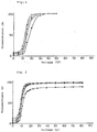
- Figs. 1, 2 and 3 are graphs showing relationships between applied voltage and transmittance of the liquid crystal display elements produced in Example 1, Example 2 and Comparative Example 1, respectively.
- the composite film in the liquid crystal display element of the present invention contains 1 to 30 % by weight of the high-boiling liquid based on the weight of the liquid crystal.
- a nematic liquid crystal such as a twisted nematic (TN) liquid crystal is used. More preferably, the liquid crystal has a larger positive dielectric constant anisotropy ⁇ to obtain the display element having good characteristics.
- TN twisted nematic
- matrix polymer which is one of the components of the composite film acrylic or methacrylic resins such as polymethyl methacrylate are used.
- an adhesive or tackifying polymer may be used to improve adhesion of the composite film to the transparent electrodes, to prevent displacement or delamination of the electrodes from the composite film and/or to make it easier to enlarge the area of the display element.
- the adhesive or tackifying polymer one having good compatibility with the matrix polymer is preferable.
- acrylic resin is used as the matrix polymer, an acrylic adhesive or tackifying polymer is preferably used. Insofar as requirements for the production of the liquid crystal display element of the present invention are satisfied, any adhesive or tackifying polymer or any combination of the adhesive or tackifying polymer and the matrix polymer may be used.
- the high-boiling liquid to be contained in the composite film comprising the liquid crystal and the matrix polymer has a boiling point of not lower than 150°C, preferably not lower than 300°C under atmospheric pressure.
- the boiling point of the high-boiling liquid is lower than 150°C, the liquid gradually evaporates off from the composite film during the use of the display element so that the response of the liquid crystal is inevitably deteriorated during long term use.
- the high-boiling liquid does not freeze at a temperature of -30 to 0°C according to surrounding environments.
- plasticizers which are generally used as plasticizers for the polymer are used since they have no adverse effect on the matrix polymer or the liquid crystal and are easily available and economical.
- alcohols, aldehydes, amines, strong acids or strong alkalis are not preferred since they have adverse effects on the matrix polymer or the liquid crystal and have poor stability.
- the high-boiling liquid is preferably contained in the liquid crystal phase in a larger amount than in the matrix polymer having a sponge-like structure.
- the high-boiling liquid is contained in the matrix polymer having the sponge-like structure in a larger amount, the strength of the composite film is decreased.
- the high-boiling liquid contained in the liquid crystal phase in a larger amount than in the matrix polymer
- the high-boiling liquid having better compatibility with the liquid crystal than with the matrix polymer
- plasticizers which have good compatibility with the nematic liquid crystal but poor compatibility with the acrylic resin (for example, di-2-ethylhexyl phthalate, diisodecyl phthalate, di-2-ethylhexyl azelate and the like) are used independently or as a mixture.
- the content of the high-boiling liquid in the composite film is from 1 to 30 % by weight, preferably 5 to 20 % by weight, more preferably about 10 % by weight based on the weight of the liquid crystal.
- the response of the liquid crystal to the applied voltage cannot be improved.
- said content exceeds 30 % by weight, the response of the liquid crystal is deteriorated.
- opacity of the liquid crystal namely a scattering degree of the light is decreased when no voltage is applied, and no clear display is achieved. Decrease of the response and the opacity may be due to excessive dilution of the liquid crystal with the high-boiling liquid.
- a dye may be added to the composite film.
- a thickness of the composite film should be larger than a wavelength of the visible light to give a light-scattering type liquid crystal display element.
- the thickness of the composite film is too larger, the driving voltage of the element becomes large. In practical, the thickness of the composite film is from 20 to 30 ⁇ m.
- an electrode comprising a transparent support such as a glass plate or a plastic film (e.g. polyethylene terephthalate (PET), polyethersulfone (PES), etc.) on which a conductive film such as ITO (indium/tin oxides) or SnO2 is formed by vapor deposition or sputtering can be used.
- a transparent conductive glass or film may be used as the electrode.
- the liquid crystal display element of the present invention may be prepared by various methods.
- the high-boiling liquid having the boiling point of not lower than 150°C, the matrix polymer and the liquid crystal are mixed with the low-boiling solvent having the boiling point of lower than 150°C to prepare a coating liquid.
- the coating liquid is applied on one transparent electrode, dried and solidified at a temperature lower than the boiling point of the high-boiling liquid to form the composite film.
- the liquid crystal display element having good response to the applied voltage can be produced by substantially the same process as the conventional process without increasing the number of the production steps. That is, the coating liquid is applied on one of the pair of transparent electrodes, dried and consolidated to from the composite film, and the other electrode is laminated on the formed composite film and thermally treated to produce the liquid crystal display element of the present invention.
- the low-boiling solvent is selected from various solvents having a boiling point of lower than 150°C according to the kinds of the matrix polymer, the liquid crystal and the high-boiling liquid to be dissolved or dispersed in the solvent.
- the low-boiling solvent one that has a boiling point as low as possible and is easily evaporated (with a high vapor pressure) is preferably used because if the low-boiling solvent is not easily evaporated and it takes long time to dry and solidify the applied coating liquid, a structure in which the liquid crystal is suitably dispersed in the sponge-like structure of the matrix polymer is not well formed.
- Amounts of the components to be added to the low-boiling solvent are not critical in the present invention and depend on a manner for applying the coating liquid on the transparent electrode, the thickness of the composite film to be formed, and the like.
- the coating liquid can be applied on the transparent electrode by a conventional method such as bar coating, spray coating, roll coating, flow coating, and the like.
- a polymer mixture of 80 parts of polymethyl methacrylate (Delpet, a trade mark of Asahi Chemical) as a matrix polymer and 20 parts of an acrylic tackifying polymer (manufactured by Teikoku Kagaku) and a liquid crystal (Type E 63 distributed by Merck Japan) in a weight ratio of the liquid crystal to the polymer mixture of 6:4 were dissolved in dichloromethane as a low-boiling solvent to a total solute concentration of 15 %.
- dichloromethane as a low-boiling solvent
- di-2-ethylhexyl azelate (DOZ) as a high-boiling liquid was added in an amount of 10 % based on the weight of the liquid crystal to prepare a coating liquid.
- the coating liquid was then coated on a transparent conductive film (ITO-polyethersulfone film having a thickness of 100 ⁇ m) with a bar, dried at room temperature for 30 minutes and then at 80°C for 30 minutes to form a composite film having a thickness of 30 ⁇ m.
- a transparent conductive film ITO-polyethersulfone film having a thickness of 100 ⁇ m
- the same transparent conductive film as above was laminated and heated at 80°C for 10 minutes to obtain a liquid crystal display element.
- a polymer mixture of 80 parts of polymethyl methacrylate (Delpet, a trade mark of Asahi Chemical) as a matrix polymer and 20 parts of an acrylic tackifying polymer (manufactured by Teikoku Kagaku) and a liquid crystal (Type E 63 distributed by Merck Japan) in a weight ratio of the liquid crystal to the polymer mixture of 6:4 were dissolved in chloroform as a low-boiling solvent to a total solute concentration of 20 %.
- diisodecyl phthalate (DIDP) as a high-boiling liquid was added in an amount of 13 % based on the weight of the liquid crystal to prepare a coating liquid.
- DIDP diisodecyl phthalate
- the coating liquid was then coated on a transparent conductive film (ITO-polyethersulfone film having a thickness of 100 vm) with a bar, dried at room temperature for 30 minutes and then at 70°C for 30 minutes to form a composite film having a thickness of 20 ⁇ m.
- a transparent conductive film ITO-polyethersulfone film having a thickness of 100 vm
- the same transparent conductive film as above was laminated and heated at 70°C for 10 minutes to obtain a liquid crystal display element.
- the coating liquid was then coated on a transparent conductive film (ITO-polyethersulfone film having a thickness of 100 ⁇ m) with a bar, dried at room temperature for 30 minutes to form a composite film having a thickness of 30 ⁇ m.
- a transparent conductive film ITO-polyethersulfone film having a thickness of 100 ⁇ m
- the same transparent conductive film as above was laminated and heated at 80°C for 10 minutes to obtain a liquid crystal display element.
- Each liquid crystal display element was set in a spectrophotometer (Type UV-160 manufactured by Shimadzu) and a sinusodial wave alternating current of 60 Hz was applied between the transparent electrodes to measure a relationship between the applied voltage and transmittance of light having various wavelengths.
- the results for Example 1, Example 2 and Comparative Example 1 are shown in Figs. 1, 2 and 3, respectively.
- the transmittance represents values corrected for absorbance through a pair of the transparent electrodes
- the voltage (V) represents the effective voltage between the transparent electrodes.
- White circles, black circles, white triangles and black triangles represent the data for light having wavelengths of 700 nm, 600 nm, 500 nm and 400 nm, respectively.
- Example 1 showed sharp change of the transmittance with the change of the applied voltage.
- the difference of the transmittance between the wavelengths, and only at the applied voltage of 30 V, the transmittance was 100 % over the whole range of visible light.
- Example 2 In the same manner as in Example 1 but using 1 % of DOZ based on the weight of the liquid crystal, a liquid crystal display element was produced and its electro-optic response was tested as in Example 1. At the applied voltage of 270 V, sufficient transmittance was achieved.
- Example 1 In the same manner as in Example 1 but using 30 % of DOZ based on the weight of the liquid crystal, a liquid crystal display element was produced and its electro-optic response was tested as in Example 1. The results were substantially the same as those in Example 1. But, in the applied voltage range of 5 V or lower, the transmittance was slightly improved.
- Example 1 In the same manner as in Example 1 but using 50 % of DOZ based on the weight of the liquid crystal, a liquid crystal display element was produced and its electro-optic response was tested as in Example 1. The element did not respond to any applied voltage and the transmittance did not change.
- Example 1 In the same manner as in Example 1 but using 0.1 % of DOZ based on the weight of the liquid crystal, a liquid crystal display element was produced and its electro-optic response was tested as in Example 1. The results were substantially the same as in Comparative Example 1 in which no DOZ was used.
Landscapes
- Chemical & Material Sciences (AREA)
- Crystallography & Structural Chemistry (AREA)
- Engineering & Computer Science (AREA)
- Materials Engineering (AREA)
- Organic Chemistry (AREA)
- Liquid Crystal (AREA)
Claims (9)
- Flüssigkristall-Anzeigeelement, umfassend ein Paar transparente Elektroden und einen Verbundfilm, der sich zwischen dem Paar der transparenten Elektroden befindet, wobei der Film ein Matrixpolymer, ausgewählt aus Acrylharzen und Methacrylharzen, ein nematisches Flüssigkristall und eine hochsiedende Flüssigkeit mit einem Siedepunkt von nicht niedriger als 150°C unter Atmosphärendruck in einer Menge von 1 bis 30 Gew.-%, bezogen auf das Gewicht des Flüssigkristalls, umfaßt.
- Flüssigkristall-Anzeigeelement gemäß Anspruch 1, in welchem die hochsiedende Flüssigkeit wenigstens eine ist, ausgewählt aus der Gruppe bestehend aus Di-2-ethylhexylphathalat, Di-isodecylphthalat und Di-2-ethylhexylacelat.
- Flüssigkristall-Anzeigeelement gemäß Anspruch 2, in welchem das nematische Flüssigkristall ein getwistetes nematisches Flüssigkristall ist.
- Flüssigkristall-Anzeigeelement gemäß Anspruch 1 oder 2, in welchem das Methacrylsäureharz Polymethylmethacrylat ist.
- Flüssigkristall-Anzeigeelement gemäß Anspruch 1, in welchem die Menge der hochsiedenden Flüssigkeit etwa 10 Gew.-%, bezogen auf das Gewicht des Flüssigkristalls beträgt.
- Flüssigkristall-Anzeigeelement gemäß Anspruch 1, in welchem die hochsiedende Flüssigkeit einen Siedepunkt von nicht niedriger als 300°C hat.
- Flüssigkristall-Anzeigeelement gemäß Anspruch 1, in welchem der Verbundfilm weiterhin einen polymeren Kleber umfaßt.
- Flüssigkristall-Anzeigeelement gemäß Anspruch 3, in welchem der Verbundfilm eine Dicke von 20 bis 30/um hat.
- Verfahren zum Herstellen des Flüssigkristall-Anzeigeelements gemäß Anspruch 1, umfassend die Stufen des Aufbringens einer Überzugsflüssigkeit, umfassend ein Matrixpolymer, ausgewählt aus Acrylharzen und Methacrylharzen, und ein nematisches Flüssigkristall, gelöst oder dispergiert in einer Mischung aus einem Lösungsmittel mit einem Siedepunkt von niedriger als 150°C und einer hochsiedenden Flüssigkeit mit einem Siedepunkt von nicht weniger als 150°C, auf die Oberfläche einer von einem Paar von transparenten Elektroden, Trocknen der aufgetragenen Flüssigkeit bei einer Temperatur, die niedriger ist als der Siedepunkt der hochsiedenden Flüssigkeit, unter Ausbildung eines Verbundfilms und Laminieren der anderen Elektrode aus dem Elektrodenpaar auf den Verbundfilm.
Applications Claiming Priority (4)
| Application Number | Priority Date | Filing Date | Title |
|---|---|---|---|
| JP250922/89 | 1989-09-26 | ||
| JP25092289 | 1989-09-26 | ||
| JP220347/90 | 1990-08-21 | ||
| JP2220347A JP2844880B2 (ja) | 1989-09-26 | 1990-08-21 | 液晶表示素子およびその製造方法 |
Publications (3)
| Publication Number | Publication Date |
|---|---|
| EP0421240A2 EP0421240A2 (de) | 1991-04-10 |
| EP0421240A3 EP0421240A3 (en) | 1992-02-19 |
| EP0421240B1 true EP0421240B1 (de) | 1996-01-31 |
Family
ID=26523657
Family Applications (1)
| Application Number | Title | Priority Date | Filing Date |
|---|---|---|---|
| EP90118391A Expired - Lifetime EP0421240B1 (de) | 1989-09-26 | 1990-09-25 | Flüssigkristallanzeige |
Country Status (3)
| Country | Link |
|---|---|
| EP (1) | EP0421240B1 (de) |
| DE (1) | DE69025118T2 (de) |
| NO (1) | NO302638B1 (de) |
Families Citing this family (6)
| Publication number | Priority date | Publication date | Assignee | Title |
|---|---|---|---|---|
| CA2131804C (en) * | 1992-03-10 | 2003-09-09 | Raychem Corporation | Encapsulated liquid crystal structures, apparatus containing the same, and methods therefor |
| US5585947A (en) * | 1994-03-24 | 1996-12-17 | Raychem Corporation | Method of making liquid crystal composite which has interfacial material disposed between liquid crystal and encapsulating medium |
| US5405551A (en) * | 1994-03-24 | 1995-04-11 | Raychem Corporation | Method of making liquid crystal composite |
| WO1996019547A1 (en) * | 1994-12-21 | 1996-06-27 | Raychem Corporation | Method of making liquid crystal composite |
| WO1999007806A1 (en) * | 1997-08-08 | 1999-02-18 | Tyco Electronics Corporation | Liquid crystal composite and device comprising same |
| JP7010401B1 (ja) | 2021-03-24 | 2022-01-26 | 凸版印刷株式会社 | 調光シート、調光シートの製造方法、および高分子分散型用液晶組成物 |
Citations (1)
| Publication number | Priority date | Publication date | Assignee | Title |
|---|---|---|---|---|
| JPH06305765A (ja) * | 1993-04-23 | 1994-11-01 | Shoei Karaaring Kk | 高濃度酸化クロム着色物とこの高濃度酸化クロム着色物に使用する高濃度酸化クロム着色剤の製造方法 |
Family Cites Families (2)
| Publication number | Priority date | Publication date | Assignee | Title |
|---|---|---|---|---|
| US4161557A (en) * | 1978-03-23 | 1979-07-17 | Liquid Crystal Products, Inc. | Polyvinyl butyral-liquid crystal film-forming composition and film |
| US4888126A (en) * | 1987-08-28 | 1989-12-19 | Linear Optics Company, Inc. | Light modulating material and method for preparing same |
-
1990
- 1990-09-25 DE DE1990625118 patent/DE69025118T2/de not_active Expired - Fee Related
- 1990-09-25 EP EP90118391A patent/EP0421240B1/de not_active Expired - Lifetime
- 1990-09-25 NO NO904175A patent/NO302638B1/no unknown
Patent Citations (1)
| Publication number | Priority date | Publication date | Assignee | Title |
|---|---|---|---|---|
| JPH06305765A (ja) * | 1993-04-23 | 1994-11-01 | Shoei Karaaring Kk | 高濃度酸化クロム着色物とこの高濃度酸化クロム着色物に使用する高濃度酸化クロム着色剤の製造方法 |
Also Published As
| Publication number | Publication date |
|---|---|
| EP0421240A3 (en) | 1992-02-19 |
| NO302638B1 (no) | 1998-03-30 |
| NO904175D0 (no) | 1990-09-25 |
| DE69025118D1 (de) | 1996-03-14 |
| DE69025118T2 (de) | 1996-07-11 |
| EP0421240A2 (de) | 1991-04-10 |
| NO904175L (no) | 1991-03-27 |
Similar Documents
| Publication | Publication Date | Title |
|---|---|---|
| JP4898701B2 (ja) | 液晶材料に基づく反射型ディスプレイ | |
| EP0204537A2 (de) | Eingekapselter Flüssigkristall mit einer smektischen Phase | |
| WO2008005202A2 (en) | Single substrate guest-host polymer liquid crystal displays | |
| JP2013011893A (ja) | 改善された特性を有する高性能可撓性ディスプレイ | |
| US7382424B2 (en) | Reflective chiral-nematic liquid crystal display with broadband reflection | |
| EP0749030A1 (de) | Flüssigkristallanzeigeelement und dessen herstellungsverfahren | |
| EP0501409B1 (de) | Flüssigkristallanzeigevorrichtung und ihre Herstellung | |
| EP0421240A2 (de) | Flüssigkristallanzeige | |
| US20020084442A1 (en) | Liquid crystal mixture and liquid crystal cell for LCDs and use of a dye with a dipole for a liquid crystal mixture | |
| US5253090A (en) | Liquid crystal electro-optic device with two materials different in refractive index dispersed in the liquid crystal | |
| US5331448A (en) | Liquid crystal display device and preparation and use thereof | |
| CN1111289C (zh) | 高反射率聚合物分散液晶光阀显示装置 | |
| US5461494A (en) | Ferroelectric liquid crystal device having colored film and protective film at non-pixel portions | |
| KR0153442B1 (ko) | 액정 디스플레이 소자 | |
| US7416684B2 (en) | Method of varying wavelengths of liquid crystals | |
| West | Liquid crystal dispersions | |
| JPH06322370A (ja) | 有機分散液晶 | |
| US7148937B2 (en) | Display comprising blended mixture of different uniform domain sizes with the ratio of smallest to largest domain size no more than 1:2 | |
| DE10111452B4 (de) | Bistabile elektrooptische Flüssigkristallanzeigen und Verfahren zu ihrer Herstellung | |
| JOHN | Liquid Crystal Dispersions | |
| WO2024203117A1 (ja) | 高分子分散型液晶フィルム | |
| KR19980029978A (ko) | 액정 표시 소자 및 그 액정층 형성방법 | |
| JPH0675207A (ja) | 液晶表示素子の製造方法 | |
| JPH07114005A (ja) | エマルジョン組成物および該組成物を用いた液晶素子 | |
| JPH04134424A (ja) | 液晶表示装置 |
Legal Events
| Date | Code | Title | Description |
|---|---|---|---|
| PUAI | Public reference made under article 153(3) epc to a published international application that has entered the european phase |
Free format text: ORIGINAL CODE: 0009012 |
|
| 17P | Request for examination filed |
Effective date: 19901220 |
|
| AK | Designated contracting states |
Kind code of ref document: A2 Designated state(s): BE DE FR GB IT NL |
|
| PUAL | Search report despatched |
Free format text: ORIGINAL CODE: 0009013 |
|
| AK | Designated contracting states |
Kind code of ref document: A3 Designated state(s): BE DE FR GB IT NL |
|
| 17Q | First examination report despatched |
Effective date: 19930816 |
|
| GRAA | (expected) grant |
Free format text: ORIGINAL CODE: 0009210 |
|
| AK | Designated contracting states |
Kind code of ref document: B1 Designated state(s): BE DE FR GB IT NL |
|
| ITF | It: translation for a ep patent filed | ||
| REF | Corresponds to: |
Ref document number: 69025118 Country of ref document: DE Date of ref document: 19960314 |
|
| ET | Fr: translation filed | ||
| PLBE | No opposition filed within time limit |
Free format text: ORIGINAL CODE: 0009261 |
|
| STAA | Information on the status of an ep patent application or granted ep patent |
Free format text: STATUS: NO OPPOSITION FILED WITHIN TIME LIMIT |
|
| 26N | No opposition filed | ||
| REG | Reference to a national code |
Ref country code: GB Ref legal event code: 746 Effective date: 19970121 |
|
| ITPR | It: changes in ownership of a european patent |
Owner name: OFF.TA DI LIC.ZA AL PUBBLICO OFF.TA AL PUBBLICO |
|
| REG | Reference to a national code |
Ref country code: FR Ref legal event code: D6 |
|
| PGFP | Annual fee paid to national office [announced via postgrant information from national office to epo] |
Ref country code: FR Payment date: 19970909 Year of fee payment: 8 |
|
| PGFP | Annual fee paid to national office [announced via postgrant information from national office to epo] |
Ref country code: GB Payment date: 19970916 Year of fee payment: 8 |
|
| PGFP | Annual fee paid to national office [announced via postgrant information from national office to epo] |
Ref country code: NL Payment date: 19970929 Year of fee payment: 8 |
|
| PGFP | Annual fee paid to national office [announced via postgrant information from national office to epo] |
Ref country code: DE Payment date: 19971010 Year of fee payment: 8 |
|
| PGFP | Annual fee paid to national office [announced via postgrant information from national office to epo] |
Ref country code: BE Payment date: 19971118 Year of fee payment: 8 |
|
| PG25 | Lapsed in a contracting state [announced via postgrant information from national office to epo] |
Ref country code: GB Free format text: LAPSE BECAUSE OF NON-PAYMENT OF DUE FEES Effective date: 19980925 |
|
| PG25 | Lapsed in a contracting state [announced via postgrant information from national office to epo] |
Ref country code: BE Free format text: LAPSE BECAUSE OF NON-PAYMENT OF DUE FEES Effective date: 19980930 |
|
| BERE | Be: lapsed |
Owner name: SUMITOMO ELECTRIC INDUSTRIES LTD Effective date: 19980930 |
|
| PG25 | Lapsed in a contracting state [announced via postgrant information from national office to epo] |
Ref country code: NL Free format text: LAPSE BECAUSE OF NON-PAYMENT OF DUE FEES Effective date: 19990401 |
|
| GBPC | Gb: european patent ceased through non-payment of renewal fee |
Effective date: 19980925 |
|
| PG25 | Lapsed in a contracting state [announced via postgrant information from national office to epo] |
Ref country code: FR Free format text: LAPSE BECAUSE OF NON-PAYMENT OF DUE FEES Effective date: 19990531 |
|
| NLV4 | Nl: lapsed or anulled due to non-payment of the annual fee |
Effective date: 19990401 |
|
| PG25 | Lapsed in a contracting state [announced via postgrant information from national office to epo] |
Ref country code: DE Free format text: LAPSE BECAUSE OF NON-PAYMENT OF DUE FEES Effective date: 19990701 |
|
| REG | Reference to a national code |
Ref country code: FR Ref legal event code: ST |
|
| PG25 | Lapsed in a contracting state [announced via postgrant information from national office to epo] |
Ref country code: IT Free format text: LAPSE BECAUSE OF NON-PAYMENT OF DUE FEES;WARNING: LAPSES OF ITALIAN PATENTS WITH EFFECTIVE DATE BEFORE 2007 MAY HAVE OCCURRED AT ANY TIME BEFORE 2007. THE CORRECT EFFECTIVE DATE MAY BE DIFFERENT FROM THE ONE RECORDED. Effective date: 20050925 |