EP0421240A2 - Flüssigkristallanzeige - Google Patents
Flüssigkristallanzeige Download PDFInfo
- Publication number
- EP0421240A2 EP0421240A2 EP90118391A EP90118391A EP0421240A2 EP 0421240 A2 EP0421240 A2 EP 0421240A2 EP 90118391 A EP90118391 A EP 90118391A EP 90118391 A EP90118391 A EP 90118391A EP 0421240 A2 EP0421240 A2 EP 0421240A2
- Authority
- EP
- European Patent Office
- Prior art keywords
- liquid crystal
- display element
- liquid
- crystal display
- boiling
- Prior art date
- Legal status (The legal status is an assumption and is not a legal conclusion. Google has not performed a legal analysis and makes no representation as to the accuracy of the status listed.)
- Granted
Links
Images
Classifications
-
- C—CHEMISTRY; METALLURGY
- C09—DYES; PAINTS; POLISHES; NATURAL RESINS; ADHESIVES; COMPOSITIONS NOT OTHERWISE PROVIDED FOR; APPLICATIONS OF MATERIALS NOT OTHERWISE PROVIDED FOR
- C09K—MATERIALS FOR MISCELLANEOUS APPLICATIONS, NOT PROVIDED FOR ELSEWHERE
- C09K19/00—Liquid crystal materials
- C09K19/52—Liquid crystal materials characterised by components which are not liquid crystals, e.g. additives with special physical aspect: solvents, solid particles
- C09K19/54—Additives having no specific mesophase characterised by their chemical composition
- C09K19/542—Macromolecular compounds
- C09K19/544—Macromolecular compounds as dispersing or encapsulating medium around the liquid crystal
Definitions
- the present invention relates to a liquid crystal display element which can be used in a liquid crystal display to be used in a TV set or an office automation equipment such as a word processor or a work station.
- liquid crystal display element which is prepared by applying a solution of a matrix polymer and a liquid crystal material in a solvent on a transparent electrode by casting, drying the applied solution to form a polymer/liquid crystal composite film on the electrode and laminating another transparent electrode on the composite film (cf. Polymer Preprints, Japan, Vol. 37, No. 8 (1988) 2450).
- the comiposite film comprises the polymeric matrix having a sponge-like structure and the liquid crystal which fills pores of the polymeric matrix. Under a no-voltage condition, liquid crystal molecules are randomly oriented in the pores so that incident light is scattered and the composite film is opaque.
- liquid crystal display element With the above described liquid crystal display element, it is easy to enlarge the area of liquid crystal display element since the element is prepared by applying and drying the solution of the matrix polymer and the liquid crystal material to form the composite film having the above electro-optic effect. Further, through the selection of a kind of the matrix polymer, flexibility is imparted to the composite film. In addition, since a flexible transparent film to which conductivity is imparted by, for example, forming a transparent conductive film thereon can be used as a transparent electrode, it is possible to impart flexibility to the liquid crystal display element.
- a similar liquid crystal display element is commercially available from Taliq Corp. (USA) under a trade name of "NCAP Liquid Crystal”.
- liquid crystal display element comprising the composite film has insufficient response to an applied voltage, it has various drawbacks that its speed of response is low and that variation of transmittance is small. Then, it is difficult to use such liquid crystal display element in a matrix driving type liquid crystal display device which is required to have high definition and high response. To achieve sufficient variation of transmittance, a driving voltage should be increased, and therefore peripheral equipments should be made resistant to high voltage.
- One object of the present invention is to provide a liquid crystal display element which comprises a composite film of a matrix polymer and a liquid crystal and has high response to applied voltage.
- Another object of the present invention is to provide a method for producing a liquid crystal display element which comprises a composite film of a matrix polymer and a liquid crystal and has high response to applied voltage.
- a liquid crystal display element comprising a pair of transparent electrodes and a composite film interposed between said pair of transparent electrodes which film comprises a matrix polymer, a liquid crystal and a high-boiling liquid having a boiling point of not lower than 150°C under atmospheric pressure in an amount of 1 to 30 % by weight based on the weight of liquid crystal.
- a method for producing a liquid crystal display element of the present invention which comprises steps of applying a coating liquid comprising a matrix polymer and a liquid crystal dissolved or dispersed in a mixture of a solvent having a boiling point lower than 150°C and a high-boiling liquid having a boiling point of not lower than 150°C on a surface of one of a pair of transparent electrodes, drying said applied liquid at a temperature of lower than the boiling point of said high-boiling liquid to form a composite film and laminating the other of said pair of transparent electrodes on said composite film.
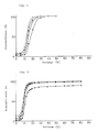
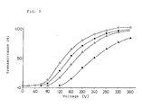
- Figs. 1, 2 and 3 are graphs showing relationships between applied voltage and transmittance of the liquid crystal display elements produced in Example 1, Example 2 and Comparative Example 1, respectively.
- the composite film in the liquid crystal display element of the present invention contains 1 to 30 % by weight of the high-boiling liquid based on the weight of the liquid crystal.
- a nematic liquid crystal such as a twisted nematic (TN) liquid crystal is preferably used, although other liquid crystals may be used. More preferably, the liquid crystal has a larger positive dielectric constant anisotropy ⁇ to obtain the display element having good characteristics.
- TN twisted nematic
- the matrix polymer which is one of the components of the composite film, one having good transparency to visible light is preferred.
- Preferred examples of the matrix polymer are acrylic or methacrylic resins such as polymethyl methacrylate.
- an adhesive or tackifying polymer may be used to improve adhesion of the composite film to the transparent electrodes, to prevent displacement or delamination of the electrodes from the composite film and/or to make it easier to enlarge the area of the display element.
- the adhesive or tackifying polymer one having good compatibility with the matrix polymer is preferable.
- an acrylic adhesive or tackifying polymer is preferably used. Insofar as requirements for the production of the liquid crystal display element of the present invention are satisfied, any adhesive or tackifying polymer or any combination of the adhesive or tackifying polymer and the matrix polymer may be used.
- the high-boiling liquid to be contained in the composite film comprising the liquid crystal and the matrix polymer has a boiling point of not lower than 150°C, preferably not lower than 300°C under atmospheric pressure.
- the boiling point of the high-boiling liquid is lower than 150°C, the liquid gradually evaporates off from the composite film during the use of the display element so that the response of the liquid crystal is inevitably deteriorated during long term use.
- the high-boiling liquid does not freeze at a temperature of -30 to 0°C according to surrounding environments.
- plasticizers which are generally used as plasticizers for the polymer are used since they have no adverse effect on the matrix polymer or the liquid crystal and are easily available and economical.
- alcohols, aldehydes, amines, strong acids or strong alkalis are not preferred since they have adverse effects on the matrix polymer or the liquid crystal and have poor stability.
- the high-boiling liquid is preferably contained in the liquid crystal phase in a larger amount than in the matrix polymer having a sponge-like structure.
- the strength of the composite film is decreased.
- the high-boiling liquid contained in the liquid crystal phase in a larger amount than in the matrix polymer
- the high-boiling liquid having better compatibility with the liquid crystal than with the matrix polymer
- plasticizers which have good compatibility with the nematic liquid crystal but poor compatibility with the acrylic resin (for example, di-2-ethylhexyl phthalate, diisodecyl phthalate, di-2-ethylhexyl azelate and the like) are used independently or as a mixture.
- the content of the high-boiling liquid in the composite film is from 1 to 30 % by weight, preferably 5 to 20 % by weight, more preferably about 10 % by weight based on the weight of the liquid crystal.
- the response of the liquid crystal to the applied voltage cannot be improved.
- the response of the liquid crystal is deteriorated.
- opacity of the liquid crystal namely a scattering degree of the light is decreased when no voltage is applied, and no clear display is achieved. Decrease of the response and the opacity may be due to excessive dilution of the liquid crystal with the high-boiling liquid.
- a dye may be added to the composite film.
- a thickness of the composite film should be larger than a wavelength of the visible light to give a light-scattering type liquid crystal display element.
- the thickness of the composite film is too larger, the driving voltage of the element becomes large. In practical, the thickness of the composite film is from 20 to 30 ⁇ m.
- an electrode comprising a transparent support such as a glass plate or a plastic film (e.g. polyethylene terephthalate (PET), polyethersulfone (PES), etc.) on which a conductive film such as ITO (indium/tin oxides) or SnO2 is formed by vapor deposition or sputtering can be used.
- a transparent conductive glass or film may be used as the electrode.
- the liquid crystal display element of the present invention may be prepared by various methods.
- the high-boiling liquid having the boiling point of not lower than 150°C, the matrix polymer and the liquid crystal are mixed with the low-boiling solvent having the boiling point of lower than 150°C to prepare a coating liquid.
- the coating liquid is applied on one transparent electrode, dried and solidified at a temperature lower than the boiling point of the high-boiling liquid to form the composite film.
- the liquid crystal display element having good response to the applied voltage can be produced by substantially the same process as the conventional process without increasing the number of the production steps. That is, the coating liquid is applied on one of the pair of transparent electrodes, dried and consolidated to from the composite film, and the other electrode is laminated on the formed composite film and thermally treated to produce the liquid crystal display element of the present invention.
- the low-boiling solvent is selected from various solvents having a boiling point of lower than 150°C according to the kinds of the matrix polymer, the liquid crystal and the high-boiling liquid to be dissolved or dispersed in the solvent.
- the low-boiling solvent one that has a boiling point as low as possible and is easily evaporated (with a high vapor pressure) is preferably used because if the low-boiling solvent is not easily evaporated and it takes long time to dry and solidify the applied coating liquid, a structure in which the liquid crystal is suitably dispersed in the sponge-like structure of the matrix polymer is not well formed.
- Amounts of the components to be added to the low-boiling solvent are not critical in the present invention and depend on a manner for applying the coating liquid on the transparent electrode, the thickness of the composite film to be formed, and the like.
- the coating liquid can be applied on the transparent electrode by a conventional method such as bar coating, spray coating, roll coating, flow coating, and the like.
- a polymer mixture of 80 parts of polymethyl methacrylate (Delpet, a trade mark of Asahi Chemical) as a matrix polymer and 20 parts of an acrylic tackifying polymer (manufactured by Teikoku Kagaku) and a liquid crystal (Type E 63 distributed by Merck Japan) in a weight ratio of the liquid crystal to the polymer mixture of 6:4 were dissolved in dichloromethane as a low-boiling solvent to a total solute concentration of 15 %.
- dichloromethane as a low-boiling solvent
- di-2-ethylhexyl azelate (DOZ) as a high-boiling liquid was added in an amount of 10 % based on the weight of the liquid crystal to prepare a coating liquid.
- the coating liquid was then coated on a transparent conductive film (ITO-polyethersulfone film having a thickness of 100 ⁇ m) with a bar, dried at room temperature for 30 minutes and then at 80°C for 30 minutes to form a composite film having a thickness of 30 ⁇ m.
- a transparent conductive film ITO-polyethersulfone film having a thickness of 100 ⁇ m
- the same transparent conductive film as above was laminated and heated at 80°C for 10 minutes to obtain a liquid crystal display element.
- a polymer mixture of 80 parts of polymethyl methacrylate (Delpet, a trade mark of Asahi Chemical) as a matrix polymer and 20 parts of an acrylic tackifying polymer (manufactured by Teikoku Kagaku) and a liquid crystal (Type E 63 distributed by Merck Japan) in a weight ratio of the liquid crystal to the polymer mixture of 6:4 were dissolved in chloroform as a low-boiling solvent to a total solute concentration of 20 %.
- diisodecyl phthalate (DIDP) as a high-boiling liquid was added in an amount of 13 % based on the weight of the liquid crystal to prepare a coating liquid.
- DIDP diisodecyl phthalate
- the coating liquid was then coated on a transparent conductive film (ITO-polyethersulfone film having a thickness of 100 vm) with a bar, dried at room temperature for 30 minutes and then at 70°C for 30 minutes to form a composite film having a thickness of 20 ⁇ m.
- a transparent conductive film ITO-polyethersulfone film having a thickness of 100 vm
- the same transparent conductive film as above was laminated and heated at 70°C for 10 minutes to obtain a liquid crystal display element.
- the coating liquid was then coated on a transparent conductive film (ITO-polyethersulfone film having a thickness of 100 ⁇ m) with a bar, dried at room temperature for 30 minutes to form a composite film having a thickness of 30 ⁇ m.
- a transparent conductive film ITO-polyethersulfone film having a thickness of 100 ⁇ m
- the same transparent conductive film as above was laminated and heated at 80°C for 10 minutes to obtain a liquid crystal display element.
- Each liquid crystal display element was set in a spectrophotometer (Type UV-160 manufactured by Shimadzu) and a sinusodial wave alternating current of 60 Hz was applied between the transparent electrodes to measure a relationship between the applied voltage and transmittance of light having various wavelengths.
- the results for Example 1, Example 2 and Comparative Example 1 are shown in Figs. 1, 2 and 3, respectively.
- the transmittance represents values corrected for absorbance through a pair of the transparent electrodes
- the voltage (V) represents the effec tive voltage between the transparent electrodes.
- White circles, black circles, white triangles and black triangles represent the data for light having wavelengths of 700 nm, 600 nm, 500 nm and 400 nm, respectively.
- Example 2 In the same manner as in Example 1 but using 1 % of DOZ based on the weight of the liquid crystal, a liquid crystal display element was produced and its electro-optic response was tested as in Example 1. At the applied voltage of 270 V, sufficient transmittance was achieved.
- Example 1 In the same manner as in Example 1 but using 30 % of DOZ based on the weight of the liquid crystal, a liquid crystal display element was produced and its electro-optic response was tested as in Example 1. The results were substantially the same as those in Example 1. But, in the applied voltage range of 5 V or lower, the transmittance was slightly improved.
- Example 1 In the same manner as in Example 1 but using 50 % of DOZ based on the weight of the liquid crystal, a liquid crystal display element was produced and its electro-optic response was tested as in Example 1. The element did not respond to any applied voltage and the transmittance did not change.
- Example 1 In the same manner as in Example 1 but using 0.1 % of DOZ based on the weight of the liquid crystal, a liquid crystal display element was produced and its electro-optic response was tested as in Example 1. The results were subs tantially the same as in Comparative Example 1 in which no DOZ was used.
Landscapes
- Chemical & Material Sciences (AREA)
- Crystallography & Structural Chemistry (AREA)
- Engineering & Computer Science (AREA)
- Materials Engineering (AREA)
- Organic Chemistry (AREA)
- Liquid Crystal (AREA)
Applications Claiming Priority (4)
| Application Number | Priority Date | Filing Date | Title |
|---|---|---|---|
| JP25092289 | 1989-09-26 | ||
| JP250922/89 | 1989-09-26 | ||
| JP2220347A JP2844880B2 (ja) | 1989-09-26 | 1990-08-21 | 液晶表示素子およびその製造方法 |
| JP220347/90 | 1990-08-21 |
Publications (3)
| Publication Number | Publication Date |
|---|---|
| EP0421240A2 true EP0421240A2 (de) | 1991-04-10 |
| EP0421240A3 EP0421240A3 (en) | 1992-02-19 |
| EP0421240B1 EP0421240B1 (de) | 1996-01-31 |
Family
ID=26523657
Family Applications (1)
| Application Number | Title | Priority Date | Filing Date |
|---|---|---|---|
| EP90118391A Expired - Lifetime EP0421240B1 (de) | 1989-09-26 | 1990-09-25 | Flüssigkristallanzeige |
Country Status (3)
| Country | Link |
|---|---|
| EP (1) | EP0421240B1 (de) |
| DE (1) | DE69025118T2 (de) |
| NO (1) | NO302638B1 (de) |
Cited By (5)
| Publication number | Priority date | Publication date | Assignee | Title |
|---|---|---|---|---|
| US5405551A (en) * | 1994-03-24 | 1995-04-11 | Raychem Corporation | Method of making liquid crystal composite |
| US5427713A (en) * | 1992-03-10 | 1995-06-27 | Raychem Corporation | Encapsulated liquid crystal structures, apparatus containing the same, and methods therefor |
| US5585947A (en) * | 1994-03-24 | 1996-12-17 | Raychem Corporation | Method of making liquid crystal composite which has interfacial material disposed between liquid crystal and encapsulating medium |
| US5830385A (en) * | 1994-12-21 | 1998-11-03 | Raychem Corporation | Method of making liquid crystal composite |
| US5951912A (en) * | 1997-08-08 | 1999-09-14 | Raychem Corporation | Liquid crystal composite and device comprising same |
Citations (4)
| Publication number | Priority date | Publication date | Assignee | Title |
|---|---|---|---|---|
| EP0004464A2 (de) * | 1978-03-23 | 1979-10-03 | Liquid Crystal Products, Inc. | Filmbildende Polyvinylbutyral-Flüssigkristall-Zusammensetzung und ihre Anwendung |
| JPS5883044A (ja) * | 1981-11-12 | 1983-05-18 | Sumitomo Naugatuck Co Ltd | 熱可塑性樹脂組成物 |
| EP0307114A2 (de) * | 1987-08-28 | 1989-03-15 | Kent State University | Lichtmodulierungsmaterial und Verfahren zu dessen Herstellung |
| JPH06305765A (ja) * | 1993-04-23 | 1994-11-01 | Shoei Karaaring Kk | 高濃度酸化クロム着色物とこの高濃度酸化クロム着色物に使用する高濃度酸化クロム着色剤の製造方法 |
-
1990
- 1990-09-25 EP EP90118391A patent/EP0421240B1/de not_active Expired - Lifetime
- 1990-09-25 DE DE1990625118 patent/DE69025118T2/de not_active Expired - Fee Related
- 1990-09-25 NO NO904175A patent/NO302638B1/no unknown
Patent Citations (4)
| Publication number | Priority date | Publication date | Assignee | Title |
|---|---|---|---|---|
| EP0004464A2 (de) * | 1978-03-23 | 1979-10-03 | Liquid Crystal Products, Inc. | Filmbildende Polyvinylbutyral-Flüssigkristall-Zusammensetzung und ihre Anwendung |
| JPS5883044A (ja) * | 1981-11-12 | 1983-05-18 | Sumitomo Naugatuck Co Ltd | 熱可塑性樹脂組成物 |
| EP0307114A2 (de) * | 1987-08-28 | 1989-03-15 | Kent State University | Lichtmodulierungsmaterial und Verfahren zu dessen Herstellung |
| JPH06305765A (ja) * | 1993-04-23 | 1994-11-01 | Shoei Karaaring Kk | 高濃度酸化クロム着色物とこの高濃度酸化クロム着色物に使用する高濃度酸化クロム着色剤の製造方法 |
Non-Patent Citations (2)
| Title |
|---|
| PATENT ABSTRACTS OF JAPAN vol. 7, no. 175 (C-179)18 May 1983 & JP-A-58 083 044 ( SUMITOMO ) 12 November 1981 * |
| RESEARCH DISCLOSURE. no. 292, August 1988, HAVANT GB page 29892; 'THE USE OF WETTING AGENTS ....' * |
Cited By (8)
| Publication number | Priority date | Publication date | Assignee | Title |
|---|---|---|---|---|
| US5427713A (en) * | 1992-03-10 | 1995-06-27 | Raychem Corporation | Encapsulated liquid crystal structures, apparatus containing the same, and methods therefor |
| US5484552A (en) * | 1992-03-10 | 1996-01-16 | Raychem Corporation | Encapsulated liquid crystal structures, apparatus containing the same, and methods therefor |
| US5571448A (en) * | 1992-03-10 | 1996-11-05 | Raychem Corporation | Encapsulated liquid crystal structures, apparatus containing the same, and methods therefor |
| US5405551A (en) * | 1994-03-24 | 1995-04-11 | Raychem Corporation | Method of making liquid crystal composite |
| US5585947A (en) * | 1994-03-24 | 1996-12-17 | Raychem Corporation | Method of making liquid crystal composite which has interfacial material disposed between liquid crystal and encapsulating medium |
| US5745198A (en) * | 1994-03-24 | 1998-04-28 | Raychem Corporation | Liquid crystal composite and method of making |
| US5830385A (en) * | 1994-12-21 | 1998-11-03 | Raychem Corporation | Method of making liquid crystal composite |
| US5951912A (en) * | 1997-08-08 | 1999-09-14 | Raychem Corporation | Liquid crystal composite and device comprising same |
Also Published As
| Publication number | Publication date |
|---|---|
| NO904175L (no) | 1991-03-27 |
| DE69025118T2 (de) | 1996-07-11 |
| EP0421240A3 (en) | 1992-02-19 |
| NO904175D0 (no) | 1990-09-25 |
| EP0421240B1 (de) | 1996-01-31 |
| NO302638B1 (no) | 1998-03-30 |
| DE69025118D1 (de) | 1996-03-14 |
Similar Documents
| Publication | Publication Date | Title |
|---|---|---|
| JP4898701B2 (ja) | 液晶材料に基づく反射型ディスプレイ | |
| US7754295B2 (en) | Single substrate guest-host polymer dispersed liquid crystal displays | |
| DE112006001664T5 (de) | Flüssigkristall-Tröpfchen in einem hydrophoben Bindemittel | |
| EP0421240B1 (de) | Flüssigkristallanzeige | |
| EP0749030A1 (de) | Flüssigkristallanzeigeelement und dessen herstellungsverfahren | |
| US20050110925A1 (en) | Reflective chiral-nematic liquid crystal display with broadband reflection | |
| US5403510A (en) | Liquid crystal display device and preparation thereof | |
| US6737126B2 (en) | Liquid crystal mixture and liquid crystal cell for LCDs and use of a dye with a dipole for a liquid crystal mixture | |
| CA2028705A1 (en) | Color liquid crystal display | |
| US5331448A (en) | Liquid crystal display device and preparation and use thereof | |
| US5461494A (en) | Ferroelectric liquid crystal device having colored film and protective film at non-pixel portions | |
| KR0153442B1 (ko) | 액정 디스플레이 소자 | |
| US7416684B2 (en) | Method of varying wavelengths of liquid crystals | |
| JPH06322370A (ja) | 有機分散液晶 | |
| DE10111452B4 (de) | Bistabile elektrooptische Flüssigkristallanzeigen und Verfahren zu ihrer Herstellung | |
| US7148937B2 (en) | Display comprising blended mixture of different uniform domain sizes with the ratio of smallest to largest domain size no more than 1:2 | |
| JPH04319911A (ja) | 液晶表示素子およびその製造方法 | |
| Klosowicz et al. | Reverse-mode PDLC layers | |
| JPH0268517A (ja) | 液晶表示素子 | |
| Crawford | Reflective liquid crystal display materials- Liquid crystal-polymer dispersions | |
| Aristov et al. | Influence of mechanical deformation on electrooptical properties of polymer dispersed liquid crystal films | |
| JP2001343648A (ja) | 液晶表示素子 | |
| JPH0675207A (ja) | 液晶表示素子の製造方法 | |
| JPH04134424A (ja) | 液晶表示装置 | |
| JPH0792452A (ja) | 液晶表示用高分子とそれを用いた液晶素子および液晶素子の製造方法 |
Legal Events
| Date | Code | Title | Description |
|---|---|---|---|
| PUAI | Public reference made under article 153(3) epc to a published international application that has entered the european phase |
Free format text: ORIGINAL CODE: 0009012 |
|
| 17P | Request for examination filed |
Effective date: 19901220 |
|
| AK | Designated contracting states |
Kind code of ref document: A2 Designated state(s): BE DE FR GB IT NL |
|
| PUAL | Search report despatched |
Free format text: ORIGINAL CODE: 0009013 |
|
| AK | Designated contracting states |
Kind code of ref document: A3 Designated state(s): BE DE FR GB IT NL |
|
| 17Q | First examination report despatched |
Effective date: 19930816 |
|
| GRAA | (expected) grant |
Free format text: ORIGINAL CODE: 0009210 |
|
| AK | Designated contracting states |
Kind code of ref document: B1 Designated state(s): BE DE FR GB IT NL |
|
| ITF | It: translation for a ep patent filed |
Owner name: JACOBACCI & PERANI S.P.A. |
|
| REF | Corresponds to: |
Ref document number: 69025118 Country of ref document: DE Date of ref document: 19960314 |
|
| ET | Fr: translation filed | ||
| PLBE | No opposition filed within time limit |
Free format text: ORIGINAL CODE: 0009261 |
|
| STAA | Information on the status of an ep patent application or granted ep patent |
Free format text: STATUS: NO OPPOSITION FILED WITHIN TIME LIMIT |
|
| 26N | No opposition filed | ||
| REG | Reference to a national code |
Ref country code: GB Ref legal event code: 746 Effective date: 19970121 |
|
| ITPR | It: changes in ownership of a european patent |
Owner name: OFF.TA DI LIC.ZA AL PUBBLICO OFF.TA AL PUBBLICO |
|
| REG | Reference to a national code |
Ref country code: FR Ref legal event code: D6 |
|
| PGFP | Annual fee paid to national office [announced via postgrant information from national office to epo] |
Ref country code: FR Payment date: 19970909 Year of fee payment: 8 |
|
| PGFP | Annual fee paid to national office [announced via postgrant information from national office to epo] |
Ref country code: GB Payment date: 19970916 Year of fee payment: 8 |
|
| PGFP | Annual fee paid to national office [announced via postgrant information from national office to epo] |
Ref country code: NL Payment date: 19970929 Year of fee payment: 8 |
|
| PGFP | Annual fee paid to national office [announced via postgrant information from national office to epo] |
Ref country code: DE Payment date: 19971010 Year of fee payment: 8 |
|
| PGFP | Annual fee paid to national office [announced via postgrant information from national office to epo] |
Ref country code: BE Payment date: 19971118 Year of fee payment: 8 |
|
| PG25 | Lapsed in a contracting state [announced via postgrant information from national office to epo] |
Ref country code: GB Free format text: LAPSE BECAUSE OF NON-PAYMENT OF DUE FEES Effective date: 19980925 |
|
| PG25 | Lapsed in a contracting state [announced via postgrant information from national office to epo] |
Ref country code: BE Free format text: LAPSE BECAUSE OF NON-PAYMENT OF DUE FEES Effective date: 19980930 |
|
| BERE | Be: lapsed |
Owner name: SUMITOMO ELECTRIC INDUSTRIES LTD Effective date: 19980930 |
|
| PG25 | Lapsed in a contracting state [announced via postgrant information from national office to epo] |
Ref country code: NL Free format text: LAPSE BECAUSE OF NON-PAYMENT OF DUE FEES Effective date: 19990401 |
|
| GBPC | Gb: european patent ceased through non-payment of renewal fee |
Effective date: 19980925 |
|
| PG25 | Lapsed in a contracting state [announced via postgrant information from national office to epo] |
Ref country code: FR Free format text: LAPSE BECAUSE OF NON-PAYMENT OF DUE FEES Effective date: 19990531 |
|
| NLV4 | Nl: lapsed or anulled due to non-payment of the annual fee |
Effective date: 19990401 |
|
| PG25 | Lapsed in a contracting state [announced via postgrant information from national office to epo] |
Ref country code: DE Free format text: LAPSE BECAUSE OF NON-PAYMENT OF DUE FEES Effective date: 19990701 |
|
| REG | Reference to a national code |
Ref country code: FR Ref legal event code: ST |
|
| PG25 | Lapsed in a contracting state [announced via postgrant information from national office to epo] |
Ref country code: IT Free format text: LAPSE BECAUSE OF NON-PAYMENT OF DUE FEES;WARNING: LAPSES OF ITALIAN PATENTS WITH EFFECTIVE DATE BEFORE 2007 MAY HAVE OCCURRED AT ANY TIME BEFORE 2007. THE CORRECT EFFECTIVE DATE MAY BE DIFFERENT FROM THE ONE RECORDED. Effective date: 20050925 |