EP0412666A2 - Lese/Schreib-Speicher - Google Patents
Lese/Schreib-Speicher Download PDFInfo
- Publication number
- EP0412666A2 EP0412666A2 EP90307789A EP90307789A EP0412666A2 EP 0412666 A2 EP0412666 A2 EP 0412666A2 EP 90307789 A EP90307789 A EP 90307789A EP 90307789 A EP90307789 A EP 90307789A EP 0412666 A2 EP0412666 A2 EP 0412666A2
- Authority
- EP
- European Patent Office
- Prior art keywords
- memory
- address
- bus
- control
- data
- Prior art date
- Legal status (The legal status is an assumption and is not a legal conclusion. Google has not performed a legal analysis and makes no representation as to the accuracy of the status listed.)
- Granted
Links
- 230000015654 memory Effects 0.000 title claims abstract description 248
- 230000004044 response Effects 0.000 claims abstract description 18
- 238000000034 method Methods 0.000 claims abstract description 14
- 230000009977 dual effect Effects 0.000 claims abstract description 7
- 230000003139 buffering effect Effects 0.000 claims description 4
- 230000001934 delay Effects 0.000 abstract description 2
- 239000000872 buffer Substances 0.000 description 37
- 238000010586 diagram Methods 0.000 description 6
- 230000007704 transition Effects 0.000 description 6
- 230000000977 initiatory effect Effects 0.000 description 5
- 230000009471 action Effects 0.000 description 4
- 230000005540 biological transmission Effects 0.000 description 4
- 230000006870 function Effects 0.000 description 2
- 230000008901 benefit Effects 0.000 description 1
- 238000004519 manufacturing process Methods 0.000 description 1
- 230000011664 signaling Effects 0.000 description 1
- 230000003068 static effect Effects 0.000 description 1
- 230000001360 synchronised effect Effects 0.000 description 1
Images

Classifications
-
- G—PHYSICS
- G11—INFORMATION STORAGE
- G11C—STATIC STORES
- G11C8/00—Arrangements for selecting an address in a digital store
- G11C8/16—Multiple access memory array, e.g. addressing one storage element via at least two independent addressing line groups
-
- G—PHYSICS
- G11—INFORMATION STORAGE
- G11C—STATIC STORES
- G11C7/00—Arrangements for writing information into, or reading information out from, a digital store
Definitions
- the present invention relates in general to a read/write memory for use with a microprocessor having improved memory access time and more specifically to a dual-port shared memory in which memory access is obtained at a speed allowing contention between microprocessors to be resolved in a manner transparent to the dual processors.
- the invention also relates to a method for communicating data between a read/write memory and a processor over a multiplexed information path.
- Random access memories are available in many different configurations and with many different features for satisfying a variety of design needs.
- Static and dynamic memory chips are available with various memory capacities and speeds. In general, a higher speed memory results in a higher cost per bit of memory capacity due to the usual need to rely on more complex circuit design and fabrication techniques.
- Dual-port memories are employed to allow sharing of a memory by a pair of separate processors. Multiple processors are frequently used in applications where the capacity or speed of a single processor is inadequate for providing the desired system operation.
- the use of a shared memory may be desirable where information or variables are used by both processors in performing their separate functions. For example, a first processor may control operation of a vehicle engine while a second processor may control a vehicle transmission.
- the separate control functions are implemented according to a plurality of sensed system parameters, some of which are used by both processors, such as engine speed, engine torque, and vehicle speed.
- a method for communicating data between a read/write memory and an electronic processor over a multiplexed information path comprising the steps of, transmitting a valid address on said information path from said processor to said memory, transmitting a signal from said processor to said memory indicating that the information transmitted on said information path is a valid address, latching said valid address in said memory, retrieving the contents at said valid address in response to said signal and without any indication whether data is to be transferred to or from said memory, storing said contents in a register, transmitting either a write request or a read request from said processor to said memory, and transferring said contents from said register to said information path in response to a read request.
- a read/write memory comprising, a memory element array (33), each element having a unique address, a memory control (26) coupled to said memory element array, a multiplexed address/data bus (22,25), a bus latch (20,23) coupled to said address/data bus (22,25), to said memory control (26), and to said memory element array (33), a control bus (21,24) coupled to said bus latch and to said memory control for conducting an address-valid signal to cause said bus latch to latch the contents conducted on said address/data bus as a memory address and for conducting a direction signal for indicating the direction of data movement for writing into or reading out from said memory, said address-valid signal being conducted on said control bus at a time prior to a corresponding direction signal, and a memory output register (28,31) coupled to said memory element array (33), to said memory control (26), and to said address/data bus (22), said memory control (26) causing the contents of said memory element array at said memory address to be transferred to said memory output
- a dual port memory comprising a first port including a first control bus for conducting a first valid-address signal and a first read signal and including first multiplexed bus means for conducting address and data signals, a second port including a second control bus for conducting a second valid-address signal and a second read signal and including second multiplexed bus means for conducting address and data signals, a plurality of memory elements randomly accessible via unique addresses through either of said ports, first register means coupled to said first port and to said memory elements for buffering data being transmitted from said memory elements to said first multiplexed bus means, second register means coupled to said second port and to said memory elements for buffering data being transmitted from said memory elements to said second multiplexed bus means, control means coupled to said first and second ports, said first and second register means, and said memory elements for controlling write and read access to said memory elements, said control means transferring data from a selected memory element to one of said register means in response to a valid-address signal on the respective one of said ports
- the dual-port memory embodying the invention operates at a sufficiently high speed to allow asynchronous access from each port without special timing actions such as handshaking or added wait states.
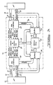
- a microprocessor system including a microprocessor 10 and a microprocessor 11.
- Microprocessor 10 is coupled via a bus 15 to a read-only memory (ROM) 12, a random access memory (RAM) 13, and a shared RAM 14.
- Microprocessor 11 is coupled via a bus 18 to a ROM 16, a RAM 17, and shared RAM 14.
- Buses 15 and 18 preferably comprise separate control buses and address/data buses.
- Most microprocessors employ a multiplexed address/data bus in order to reduce the number of external chip connections (i.e., pin outs) to a manageable number.
- microprocessor 10 and microprocessor 11 will attempt access to shared RAM 14 simultaneously.
- memory designs which allow simultaneous access to the memory through a plurality of ports.
- these designs suffer from disadvantages in complexity, cost, and size for a given memory capacity. It is also known from the prior art to provide contention resolution when simultaneous requests for memory access occur.
- Arbitration of a memory contention can be resolved on a first come, first serve basis or can be accomplished by establishing predetermined time slots for access through each respective port (i.e., time multiplexing).
- time multiplexing i.e., time multiplexing
- Memory contention can be handled by handshaking techniques in which a separate request line is provided between each microprocessor and the shared memory.
- the memory arbitrates the requests and grants access directly to a respective microprocessor via separate grant lines connected between the memory and each microprocessor.
- After a microprocessor issues a memory access request it monitors its grant line until it is granted memory access. It can then proceed as though it were the only microprocessor connected to the memory. However, efficiency is lost because the delay in being granted access can be long.
- wait states in the operation of the microprocessors to provide sufficient time for arbitrated access by two ports.
- wait states also reduce efficiency as will become more apparent from consideration of the timing diagrams of figure 2 which correspond to an arbitrary microprocessor instruction.
- the execution of a microprocessor instruction is performed during an instruction cycle which is determined by an operation code for that instruction.
- Each instruction cycle includes a plurality of machine states (numbered T1, T2, T3, ...) corresponding to cycles of the microprocessor system clock.
- the timing diagram of figure 2A illustrates the timing of several signals during a memory read operation at the end of an instruction cycle.
- a clock signal CLK defines machine states T7, T8, and T9 of one instruction cycle and machine states T1 onward for a next instruction cycle.
- the contents of the multiplexed address/data bus are shown along with two control signals, namely, an address latch enable ALE signal for indicating that a valid address is contained on the bus, and an inverted read signal RD/ for signalling that data is to be read from memory and placed on the bus (a slash at the end of a signal designation indicates that the corresponding logic variable is true when the signal is low).
- an address corresponding to a location in memory is placed on the bus by the microprocessor during machine state T7.
- the ALE signal is also initiated during machine state T7 and the memory latches the address for further processing during the negative transition of the ALE signal.
- the microprocessor indicates that data is to be read from the latched address by initiating a negative transition of the RD/ signal. After a delay 19 corresponding to the memory access time, the retrieved contents from the memory location are placed on the bus by the memory as output data.
- the microprocessor latches the data from the bus at the time of the positive transition in the RD/ signal. Thus, the data must be ready on the bus at the time expected by the microprocessor.
- the positive transition in the RD/ signal coincides with a positive transition in the CLK signal.
- wait states can be inserted between the initiation of the read request and latching of the data by the microprocessor, as shown in figure 2B.
- a memory access time 21 is shown which is greater than 1-1/2 clock cycles. Therefore, two wait states T8 and T9 are inserted so that data is latched by the microprocessor at the positive transition in the CLK signal during machine state T10.
- the microprocessor is unable to conduct other tasks and the speed at which the microprocessor executes its program is reduced.
- Memory access times 19 and 21 are measured in figures 2A and 2B from the beginning of machine state T8 corresponding to the initiation of the read signal.
- no memory access is initiated prior to receipt of the read signal since it is not known whether the latched address is to be read from or written to.
- a time period 20 between the latching of the address on the bus until the issuing of the read signal transpires during which the memory takes no action.
- this time period can be used by the memory in order to improve apparent memory response time.
- a signal is transmitted by the microprocessor indicating that a valid address has been placed on the address bus, that address is latched in a storage register within the memory.
- the address corresponds to a memory location within the memory
- the contents at that address are retrieved prior to receiving any indication whether data is to be transferred to or read from the memory address.
- the contents are stored in a register.
- the microprocessor transmits either a write command or a read command to the memory.
- the stored register contents corresponding to the address are immediately transferred from the register to the data bus. If a write request is received, the register contents are ignored.
- memory read cycle timing is improved by the data prefetch feature of the foregoing method.
- the most critical memory cycle is the read cycle. This is because a typical microprocessor may require data to be outputted to the data bus in less than 70 nanoseconds after a read request is issued. In the case of a contention arising by simultaneous requests from two microprocessors, the two requests have to be satisfied within the 70 nanosecond requirement.
- the data prefetch feature solves this problem by prefetching and storing data in a register as soon as the address is valid and before any actual read or write requests are issued by the microprocessor. If a read request is then issued, the data is merely driven onto the bus from the storage register. If a write request is issued, the prefetched data is ignored and a normal write cycle is executed.
- the data prefetch feature allows an additional half clock cycle for contention resolution and memory access, and will allow the use of slower memory devices while maintaining the full transparency feature.
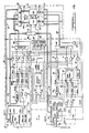
- Microprocessor 10 is coupled to port A via bus 15 which includes a control bus 21 and a multiplexed address/data bus 22.
- Control bus 21 is coupled to a bus interface 20 in port A.
- Address/data bus 22 is coupled to bus interface 20 and to memory buffers 28.
- An address bus 27 couples bus interface 20 to buffers 28.
- Microprocessor 11 is coupled to port B of shared RAM 14 via bus 18 which includes a control bus 24 and an address/data bus 25.
- Control bus 24 is coupled to a bus interface 23 in port B.
- Address/data bus 25 is coupled to bus interface 23 and to memory buffers 31.
- Bus interface 23 is coupled to buffers 31 via an address bus 30.
- Bus interface 20 and bus interface 23 are each coupled to a control and arbitration circuit 26 which controls the operation of a memory array 33 and memory buffers 28 and 31 by signals communicated over a control bus 32.
- Memory array 33 is further coupled to memory buffers 28 and 31.
- Memory array 33 is preferably configured to have a low byte and a high byte corresponding to even and odd memory addresses, respectively, in a word organised memory. Thus, reading from and writing to the memory array can be to either the low byte or high byte at a particular address.
- the control lines connected between each bus interface and the control and arbitration circuit 26 include a READ request line, a WRITE LOW request line, and a WRITE HIGH request line. READ DONE and WRITE DONE lines are connected from control and arbitration circuit 26 to each bus interface for resetting a memory access request after servicing.
- Control bus 21 includes an address-valid control line, and this line is switched to a level indicating that a valid address is on bus 22.
- bus interface 20 latches the address on bus 22 and examines the address to determine whether the address is within the range of addresses which are accessible to it in memory array 33. If the address is in range, bus interface 20 issues a READ signal to control and arbitration circuit 26 to request the reading of the contents of the address which are provided by bus interface 20 to memory buffer 28 over address bus 27.
- control and arbitration circuit 26 issues a control signal over control bus 32 to enable reading of memory array 33 through buffers 28.
- the data is read from memory array 33 into buffers 28 and is stored there until a further control signal is received from microprocessor 10 to indicate whether the memory access by microprocessor 10 is a READ or a WRITE. If a READ signal is received from microprocessor 10, buffers 28 are enabled via control and arbitration circuit 26 to drive address/data bus 22 with the retrieved data stored in buffers 28. If a WRITE signal is received from microprocessor 10, bus interface initiates a further memory access request to control and arbitration circuit 26 to write the high or low byte in memory array 33. The data to be written is latched from address/data bus 22 into buffers 28 and is then written into memory array 33 upon granting of access by control and arbitration circuit 26.
- port A is shown having a configuration for interfacing to the 80C196 microcontroller manufactured by Intel Corporation and port B is shown having a configuration for interfacing with an Intel 8061 Microcontroller.
- port B is shown having a configuration for interfacing with an Intel 8061 Microcontroller.
- FIG 4 a dual-port, asynchronous memory is shown in figure 4, it will be understood that memories having fewer or greater number of ports or with synchronous access can likewise benefit from the data prefetch feature of the present invention.
- Address/data bus 22 is coupled to an address latch 40 in bus interface 20 for port A.
- bus 22 is a 16-bit bi-directional multiplexed address/data bus.
- Bus 22 is further coupled to buffer 28.
- Control bus 21 included in port A comprises an address valid line 41 coupled to the clock input of latch 40, and instruction line 42 coupled to the clear input of latch 40, a WRITE LOW line 43 connected to one input of an AND gate 46, a WRITE HIGH line 44 connected to one input of an AND gate 47, and a READ line 100 coupled to one input of an AND gate 101.
- the latched address output of latch 40 is connected to an address bus 27 which is further connected to a decode circuit 45 and an address decoder and driver 90.
- Decode circuit 45 preferably includes a plurality of comparators for checking the value of the address and for providing a RANGE signal to the SET input of a READ latch 48, to another input of AND gate 46, to another input of AND gate 47, and to another input of AND gate 101.
- the output of AND gate 46 is connected to the SET input of a WRITE latch 50 and the output of AND gate 47 is connected to the SET input of a WRITE latch 51.
- the reset inputs of latches 48, 50, and 51 are connected to the output of a delay circuit 75 in control and arbitration circuit 26 which provides a RESET signal as will be described below.
- Latches 48, 50, and 51 preferably are comprised of D flip-flops.
- READ latch 48 is connected to one input of an OR gate 65 and to one input of an AND gate 70.
- the output of WRITE latch 50 is connected to another input of OR gate 65 and to an input of AND gate 71.
- the output of WRITE latch 51 is connected to another input of OR gate 65 and to one input of an AND gate 72.
- the output of OR gate 65 is connected to one input of an arbitration circuit 67 which may be comprised of a 74F786 bus arbiter integrated circuit manufactured by Signetics Corporation.
- Arbitration circuit 67 provides an AWON signal to indicate whether port A has been granted access to the memory.
- the AWON output is connected to the remaining inputs of AND gates 70, 71, and 72, and one input of an OR gate 83.
- the outputs of AND gates 70, 71, and 72 are each connected to respective inputs of an I/0 control 73 and respective inputs of an OR gate 74.
- the output of OR gate 74 is coupled to the input of delay circuit 75.
- the output of AND gate 101 is connected to memory buffer 28.
- the output of AND gate 70 is further connected to one input of an OR gate 84.
- the output of AND gate 71 is further connected to one input of an OR gate 85.
- the output of AND gate 72 is further connected to one input of an OR gate 86.
- I/O control 73 The output of I/O control 73 is connected to a port A control bus 32A which is further connected to a low-byte buffer 94 and to a high-byte buffer 95 both included in buffer 28.
- address/data bus 25 is an 8-bit bi-directional multiplexed address/data bus (commonly referred to as an MBUS) and is connected to the inputs of an address latch 52 and to memory buffer 31.
- Control bus 24 includes a strobe line 53 connected to the clock input of a shift register 55, an instruction line 54 connected to the clear input of shift register 55 and the clear input of address latch 52, and a data-in line 102 which is connected to one input of an AND gate 103 and to the D inputs of a pair of latches 60 and 61.
- Shift register 55 is configured such that its outputs ST1, ST2, ST3, and ST4 go HIGH in sequence when shift register 55 is clocked by strobe line 53. All outputs are restored to a LOW value when shift register 55 1 is connected to a LOW address byte clock input of latch 52.
- the ST2 output of shift register 55 connected to the HIGH address byte clock input of latch 52.
- the ST3 output is connected to one input of an AND gate 57 and output ST4 is connected one input of an AND gate 58.
- the latched addressed output of address latch 52 is provided on a 16-bit address bus 30 which is also connected to a decode circuit 56 and to address decoder and driver 90.
- the least significant bit of address bus 30 is further connected to a byte select circuit 63.
- Decode circuit 56 preferably includes two 8-bit comparators for decoding the address on address bus 30 and determining whether the address is within the range accessible by port B.
- a RANGE output signal is provided from decode circuit 56 to the SET input of a READ latch 62, to another input of AND gate 57, to another input of AND gate 58, and to another input of AND gate 103.
- the output of AND gate 57 is connected to the clock input of a WRITE latch 60.
- the output of AND gate 58 is connected to the clock input of a WRITE latch 61.
- the reset inputs of latches 60, 61, and 62 are each connected to the output of a delay circuit 82 for providing a RESET signal.
- Latches 60, 61, and 62 preferably are comprised of D flip-flops.
- the output of WRITE latch 60 provides a WR1 signal to byte select circuit 63 for indicating the timing of a first write operation.
- the output of WRITE latch 62 provides a WR2 signal to byte select circuit 63 for providing the timing of a second write operation.
- READ latch 62 is connected to one input of an AND gate 76 and to one input of an OR gate 66.
- a low-byte output from byte select circuit 63 is connected to one input of an AND gate 77 and to another input of OR gate 66.
- a high-byte output of byte select circuit 63 is connected to one input of an AND gate 78 and to another input of OR gate 66.
- the output of OR gate 66 is connected to a port B request input of arbitration circuit 67.
- a BWON signal is provided from arbitration circuit 67 to an input of OR gate 83 and to the remaining inputs of AND gates 76, 77, and 78.
- the output of AND gate 76 is connected to one input of an OR gate 81, an input of an OR gate 84, and an input of an I/O control 80.
- the output of AND gate 77 is connected to another input of OR gate 81, another input of OR gate 85, and another input of I/O control 80.
- the output of AND gate 78 is connected to another input of OR gate 81, another input of OR gate 86, and another input of I/O control 80.
- the output of OR gate 81 is connected to delay circuit 82.
- I/O control 80 is connected to a port B control bus 32B which is connected to low byte buffer 96 and high byte buffer 97 included in memory buffer 31.
- OR gates 83, 84, 85, and 86 are connected to a memory control 87 which provides outputs on control bus 32C that is also connected to memory array 33.
- Memory array 33 includes a low byte portion 92 and a high byte portion 93.
- Address decoder and driver 90 is connected to a memory control bus 91 for driving memory array 33. This type of memory configuration and memory control are known in the art.
- Low byte portion 92 of memory array 33 is connected to port A low byte buffer 94 through a bus 34L.
- High byte portion 93 is connected to port A high byte buffer 95 through a bus 34H.
- Low byte portion 92 is connected to port B low byte buffer 96 through a bus 35L.
- High byte portion 93 of memory array 33 is connected to port B high byte buffer 97 through a bus 35H.
- Memory access by port A will be considered first.
- a signal on instruction line 42 indicating the new instruction cycle clears address latch 40.
- the microprocessor attached to port A attempts to access memory by placing the desired memory address on bus 22.
- the microprocessor then initiates the ADDRESS VALID signal on ADDRESS VALID line 41, which clocks address latch 40 so that the address on bus 22 is latched in address latch 40.
- Latch 40 drives bus 27 with the latched address which is then received by decode circuit 45.
- Decode circuit 45 compares the address on bus 27 with a predetermined range of addresses corresponding to the accessible locations in memory array 33. If the address is in range, the RANGE signal sets READ latch 48 high and enables AND gates 46 and 47, which act as transmission gates for write lines 43 and 44. When READ latch 48 is set, its output causes the output of OR gate 65 to initiate the action of arbitration circuit 67. As soon as there are no other prior access requests still pending, arbitration circuit 67 grants memory access to port A by causing the AWON signal to go high. The AWON signal enables memory control 87 through chip enable OR gate 33.
- control signals on control bus 32A configure memory buffer 28 to receive data from memory array 33.
- the memory address corresponding to the desired read operation is contained in address decoder and driver 90 from bus 27.
- Memory control 87 sends control signals over control bus 32C for initiating the read operation.
- the contents of memory array 33 at the latched address are transferred to memory buffer 28.
- a READ signal received on read line 100 goes high. Since the RANGE signal is high, the output of AND gate 101 also goes high. A high level signal is transmitted from AND gate 101 to memory buffer 28. The high signal configures memory buffer 28 to drive the previously received memory contents onto address/data bus 22.
- delay circuit 75 After a predetermined delay time corresponding to the known time period required to access memory array 33 and store the memory contents in buffer 28, delay circuit 75 produces a RESET signal for resetting latches 48, 50, and 51, thus removing the memory access request signal from the output of OR gate 65.
- the data to be written to the already latched memory address is placed on bus 22 by the microprocessor.
- the RANGE signal continues at a high level from decode circuit 45 and transmission AND gates 46 and 47 continue to be enabled.
- a WRITE signal on write low line 43 or write high line 44 is thus transmitted to a respective write latch 50 or 51.
- the output of write latch 50 or 51 then initiates a memory access request through OR gate 65 to arbitration circuit 67.
- memory control 87 receives a memory enable signal through chip select OR gate 83.
- AND gate 71 or 72 then have both inputs at a high level thus causing one of their outputs to also go to a high level.
- the high output from AND gate 71 or 72 initiates a write low or a write high signal to memory control 87 through OR gates 85 or 86.
- the high output from AND gate 71 or 72 also causes I/O control 73 to cause memory buffer 28 to latch the data contents of bus 22 for writing to memory array 33.
- the high output of AND gate 71 or 72 also initiates the delay timing of delay circuit 75 through OR gate 74.
- Memory control 87 causes the latched contents of memory buffer 28 to be transferred to the address specified in address decoder and driver 90 from either low byte buffer 94 or high byte buffer 95 and over the appropriate bus 34L or 34H.
- write latch 50 or write latch 5I is reset by the RESET signal and the output of the write latch returns to a low level thus removing the memory access request from arbitration circuit 67.
- the output of OR gate 83 disables memory control 87 and the outputs of AND gates 70, 71, and 72 disable I/O control 73.
- the READ signal on read line 100 returns to a low level thus disabling the output of AND gate 101 and preventing memory buffer 38 from driving data onto bus 22.
- a succeeding instruction begins and causes address latch 40 to be cleared and the RANGE signal from decode circuit 45 to go low. Port A is then ready to receive another memory access request.
- port B is substantially identical to the operation of port A, except that the interface to the microprocessor is different since port B is configured to host the 8061 microcontroller.
- bus 25 is an 8-bit multiplexed address/data bus so that one-half of each 16-bit address in memory or a 33 is latched in succession.
- Control bus 24 includes a strobe line 53 for carrying strobe pulses for defining times that addresses and data are valid on bus 25.
- the strobe pulses are decoded by a serial-in, parallel-out shift register having its clock input connected to strobe line 53.
- the data input of shift register 55 is connected to a high level voltage (not shown). Shift register 55 is initially reset by the INSTRUCTION signal on instruction line 54.
- each pulse on strobe line 53 causes outputs ST1, ST2, ST3, and ST4 to sequentially assume a high level.
- ST1 causes address latch 52 to latch the low byte portion of an address being transmitted over bus 25.
- ST2 clocks latch 52 in order to latch the high byte portion of the address.
- the latched 16-bit address is placed on address bus 30 and is decoded by decoder circuit 56.
- the address is compared with the predetermined range of addresses and a RANGE signal is provided to read latch 62.
- An in-range address causes a reading of the high or low byte pointed to by the address on address bus 30 in the same manner as described above with regard to port A.
- the memory contents at the address specified through port B are retrieved and are stored in the corresponding portion of memory buffer 31. If the microprocessor connected to port B is attempting a read operation, a DI signal will be transmitted on the data-in line 101 causing the output of AND gate 103 to go high which causes the contents of memory buffer 31 to be driven onto address/data bus 25.
- a first byte to be written to memory is placed on bus 25.
- the microprocessor initiates a strobe pulse on line 53 which appears as an ST3 output from shift register 55.
- the output of AND gate 57 clocks write latch 60. If signal DI on line 102 indicates a write operation, then an output signal from write latch 60 is provided to byte select circuit 63 to indicate that a first byte of data is to be written to memory array 33.
- the first byte to be written can be either a high byte or a low byte depending on the value of the least significant bit of the 16-bit address.
- the least significant bit (LSB) is provided to byte select circuit 63. Either a low byte output or a high byte output from byte select circuit 63 goes high depending on the value of LSB.
- the high signal generated by byte select circuit 63 is connected to either AND gate 77 or AND gate 78 and to an input of OR gate 66. Subsequent operation of the write cycle is substantially identical to the write cycle described for port A.
- the microprocessor places the appropriate data on bus 25 and initiates another strobe pulse on strobe line 53.
- the ST4 output of shift register 55 is transmitted through AND gate 58 and clocks write latch 6I. Assuming signal DI is still high, an output signal from write latch 61 is transmitted to byte select circuit 63 to indicate that a second byte is to be written to memory array 33.
- Byte select circuit 63 selects the proper low or high byte within the same word-aligned boundary by toggling the LSB of the address and the write operation continues as with the first write operation.
- the most critical memory cycle is the read cycle since both read requests may have to be satisfied within the time period corresponding to the shortest read response specification of the microprocessors hosted by the shared memory.
- the data prefetch feature described above maintains full transparency of the dual port nature of the memory by enabling all memory access requests to be satisfied in the shortest possible time. Increased memory access speeds are achieved without any substantial increase in the cost of the memory. Wait states and handshaking techniques are avoided in the hosted microprocessors and high operating efficiency is maintained.
Landscapes
- Engineering & Computer Science (AREA)
- Microelectronics & Electronic Packaging (AREA)
- Bus Control (AREA)
- Multi Processors (AREA)
- Memory System (AREA)
Applications Claiming Priority (2)
| Application Number | Priority Date | Filing Date | Title |
|---|---|---|---|
| US390952 | 1989-08-09 | ||
| US07/390,952 US4967398A (en) | 1989-08-09 | 1989-08-09 | Read/write random access memory with data prefetch |
Publications (3)
| Publication Number | Publication Date |
|---|---|
| EP0412666A2 true EP0412666A2 (de) | 1991-02-13 |
| EP0412666A3 EP0412666A3 (en) | 1992-12-23 |
| EP0412666B1 EP0412666B1 (de) | 1995-08-09 |
Family
ID=23544622
Family Applications (1)
| Application Number | Title | Priority Date | Filing Date |
|---|---|---|---|
| EP90307789A Expired - Lifetime EP0412666B1 (de) | 1989-08-09 | 1990-07-17 | Lese/Schreib-Speicher |
Country Status (5)
| Country | Link |
|---|---|
| US (1) | US4967398A (de) |
| EP (1) | EP0412666B1 (de) |
| JP (1) | JPH03129548A (de) |
| CA (1) | CA2018503C (de) |
| DE (1) | DE69021461T2 (de) |
Cited By (2)
| Publication number | Priority date | Publication date | Assignee | Title |
|---|---|---|---|---|
| FR2719683A1 (fr) * | 1994-05-05 | 1995-11-10 | Renault | Procédé pour augmenter les capacités d'un calculateur embarqué sur un véhicule automobile. |
| EP0747789A2 (de) * | 1995-06-05 | 1996-12-11 | Canon Kabushiki Kaisha | Automatisierungssystem für Produktionsanlage |
Families Citing this family (37)
| Publication number | Priority date | Publication date | Assignee | Title |
|---|---|---|---|---|
| US5155812A (en) * | 1989-05-04 | 1992-10-13 | Texas Instruments Incorporated | Devices and method for generating and using systems, software waitstates on address boundaries in data processing |
| US5247649A (en) * | 1988-05-06 | 1993-09-21 | Hitachi, Ltd. | Multi-processor system having a multi-port cache memory |
| US6253307B1 (en) | 1989-05-04 | 2001-06-26 | Texas Instruments Incorporated | Data processing device with mask and status bits for selecting a set of status conditions |
| DE69023395T2 (de) * | 1989-06-14 | 1996-05-15 | Matsushita Electric Ind Co Ltd | Arbitrierungsschaltung. |
| US5105387A (en) * | 1989-10-13 | 1992-04-14 | Texas Instruments Incorporated | Three transistor dual port dynamic random access memory gain cell |
| US5115411A (en) * | 1990-06-06 | 1992-05-19 | Ncr Corporation | Dual port memory system |
| JP2719852B2 (ja) * | 1991-03-07 | 1998-02-25 | 三菱電機株式会社 | 半導体記憶装置およびそれからのデータ読出方法 |
| JP2673390B2 (ja) * | 1991-03-13 | 1997-11-05 | 三菱電機株式会社 | マルチポートメモリ |
| US5130769A (en) * | 1991-05-16 | 1992-07-14 | Motorola, Inc. | Nonvolatile memory cell |
| US5267199A (en) * | 1991-06-28 | 1993-11-30 | Digital Equipment Corporation | Apparatus for simultaneous write access to a single bit memory |
| US5392412A (en) * | 1991-10-03 | 1995-02-21 | Standard Microsystems Corporation | Data communication controller for use with a single-port data packet buffer |
| US5375250A (en) * | 1992-07-13 | 1994-12-20 | Van Den Heuvel; Raymond C. | Method of intelligent computing and neural-like processing of time and space functions |
| EP0600623B1 (de) * | 1992-12-03 | 1998-01-21 | Advanced Micro Devices, Inc. | Servoregelkreissteuerung |
| US5511024A (en) * | 1993-06-02 | 1996-04-23 | Rambus, Inc. | Dynamic random access memory system |
| GB9315753D0 (en) * | 1993-07-30 | 1993-09-15 | Communicate Ltd | Digital communication unit monitoring |
| US5375089A (en) * | 1993-10-05 | 1994-12-20 | Advanced Micro Devices, Inc. | Plural port memory system utilizing a memory having a read port and a write port |
| US5398211A (en) * | 1993-10-14 | 1995-03-14 | Integrated Device Technology, Inc. | Structure and method for providing prioritized arbitration in a dual port memory |
| EP2105841A1 (de) * | 1997-10-10 | 2009-09-30 | Rambus Inc. | Vorrichtung und Verfahren für Pipeline-Speicherbetrieb mit Schreib-Maskierung |
| EP1046172B1 (de) * | 1998-09-25 | 2003-08-06 | Koninklijke Philips Electronics N.V. | Schaltkreis mit pseudo-mehrport-speicher |
| US6141710A (en) * | 1998-12-15 | 2000-10-31 | Daimlerchrysler Corporation | Interfacing vehicle data bus to intelligent transportation system (ITS) data bus via a gateway module |
| US7120761B2 (en) | 2000-12-20 | 2006-10-10 | Fujitsu Limited | Multi-port memory based on DRAM core |
| KR100432218B1 (ko) * | 2001-07-28 | 2004-05-22 | 삼성전자주식회사 | 데이타 액세스 타이밍을 조정하는 듀얼 포트 메모리콘트롤러 |
| KR100441606B1 (ko) * | 2001-10-05 | 2004-07-23 | 삼성전자주식회사 | 복수의 모듈들간의 데이터 송수신 시스템 및 송수신제어방법 |
| US6717834B2 (en) * | 2002-03-26 | 2004-04-06 | Intel Corporation | Dual bus memory controller |
| KR100474704B1 (ko) * | 2002-04-29 | 2005-03-08 | 삼성전자주식회사 | 데이터의 버스트 동시쓰기가 가능한 프로세서 이중화 장치 |
| US6920510B2 (en) * | 2002-06-05 | 2005-07-19 | Lsi Logic Corporation | Time sharing a single port memory among a plurality of ports |
| US7421559B1 (en) * | 2003-12-18 | 2008-09-02 | Cypress Semiconductor Corporation | Apparatus and method for a synchronous multi-port memory |
| JP2006072935A (ja) * | 2004-09-06 | 2006-03-16 | Fujitsu Ltd | 半導体装置及びデータ書き込み制御方法 |
| KR100688537B1 (ko) * | 2005-03-16 | 2007-03-02 | 삼성전자주식회사 | 다수개의 프로세서들에 억세스 가능한 메모리 장치를 갖는시스템 |
| KR101153712B1 (ko) * | 2005-09-27 | 2012-07-03 | 삼성전자주식회사 | 멀티-포트 sdram 엑세스 제어장치와 제어방법 |
| US7962698B1 (en) | 2005-10-03 | 2011-06-14 | Cypress Semiconductor Corporation | Deterministic collision detection |
| JP4419943B2 (ja) * | 2005-11-11 | 2010-02-24 | 株式会社デンソー | Cpu間データ転送装置 |
| KR100735612B1 (ko) * | 2005-12-22 | 2007-07-04 | 삼성전자주식회사 | 멀티패쓰 억세스블 반도체 메모리 장치 |
| KR100655081B1 (ko) * | 2005-12-22 | 2006-12-08 | 삼성전자주식회사 | 가변적 액세스 경로를 가지는 멀티 포트 반도체 메모리장치 및 그에 따른 방법 |
| KR100788980B1 (ko) * | 2006-02-03 | 2007-12-27 | 엠텍비젼 주식회사 | 휴대형 장치 및 공유 메모리의 저전력 모드 제어 방법 |
| KR100745374B1 (ko) * | 2006-02-21 | 2007-08-02 | 삼성전자주식회사 | 멀티포트 반도체 메모리 장치 및 그에 따른 신호 입출력방법 |
| CN110825312B (zh) * | 2018-08-10 | 2023-06-23 | 昆仑芯(北京)科技有限公司 | 数据处理装置、人工智能芯片及电子设备 |
Citations (2)
| Publication number | Priority date | Publication date | Assignee | Title |
|---|---|---|---|---|
| EP0199134A2 (de) * | 1985-04-15 | 1986-10-29 | International Business Machines Corporation | Speichersystem mit hoher Leistung |
| EP0272869A2 (de) * | 1986-12-19 | 1988-06-29 | Fujitsu Limited | Halbleiterspeicher mit Doppelzugriffseinrichtung zur Realisierung eines Lesebetriebs mit hoher Geschwindigkeit |
Family Cites Families (6)
| Publication number | Priority date | Publication date | Assignee | Title |
|---|---|---|---|---|
| US4541076A (en) * | 1982-05-13 | 1985-09-10 | Storage Technology Corporation | Dual port CMOS random access memory |
| US4616310A (en) * | 1983-05-20 | 1986-10-07 | International Business Machines Corporation | Communicating random access memory |
| US4610004A (en) * | 1984-10-10 | 1986-09-02 | Advanced Micro Devices, Inc. | Expandable four-port register file |
| US4623990A (en) * | 1984-10-31 | 1986-11-18 | Advanced Micro Devices, Inc. | Dual-port read/write RAM with single array |
| US4660177A (en) * | 1985-01-14 | 1987-04-21 | American Telephone And Telegraph Company | Dual port complementary memory |
| US4627030A (en) * | 1985-02-04 | 1986-12-02 | At&T Bell Laboratories | Dual port memory word size expansion technique |
-
1989
- 1989-08-09 US US07/390,952 patent/US4967398A/en not_active Expired - Fee Related
-
1990
- 1990-06-07 CA CA002018503A patent/CA2018503C/en not_active Expired - Fee Related
- 1990-07-17 DE DE69021461T patent/DE69021461T2/de not_active Expired - Fee Related
- 1990-07-17 EP EP90307789A patent/EP0412666B1/de not_active Expired - Lifetime
- 1990-08-08 JP JP2210163A patent/JPH03129548A/ja active Pending
Patent Citations (2)
| Publication number | Priority date | Publication date | Assignee | Title |
|---|---|---|---|---|
| EP0199134A2 (de) * | 1985-04-15 | 1986-10-29 | International Business Machines Corporation | Speichersystem mit hoher Leistung |
| EP0272869A2 (de) * | 1986-12-19 | 1988-06-29 | Fujitsu Limited | Halbleiterspeicher mit Doppelzugriffseinrichtung zur Realisierung eines Lesebetriebs mit hoher Geschwindigkeit |
Cited By (4)
| Publication number | Priority date | Publication date | Assignee | Title |
|---|---|---|---|---|
| FR2719683A1 (fr) * | 1994-05-05 | 1995-11-10 | Renault | Procédé pour augmenter les capacités d'un calculateur embarqué sur un véhicule automobile. |
| EP0747789A2 (de) * | 1995-06-05 | 1996-12-11 | Canon Kabushiki Kaisha | Automatisierungssystem für Produktionsanlage |
| EP0747789A3 (de) * | 1995-06-05 | 1998-01-21 | Canon Kabushiki Kaisha | Automatisierungssystem für Produktionsanlage |
| US5896292A (en) * | 1995-06-05 | 1999-04-20 | Canon Kabushiki Kaisha | Automated system for production facility |
Also Published As
| Publication number | Publication date |
|---|---|
| JPH03129548A (ja) | 1991-06-03 |
| DE69021461T2 (de) | 1996-01-25 |
| CA2018503C (en) | 1997-12-09 |
| DE69021461D1 (de) | 1995-09-14 |
| EP0412666B1 (de) | 1995-08-09 |
| US4967398A (en) | 1990-10-30 |
| CA2018503A1 (en) | 1991-02-09 |
| EP0412666A3 (en) | 1992-12-23 |
Similar Documents
| Publication | Publication Date | Title |
|---|---|---|
| EP0412666B1 (de) | Lese/Schreib-Speicher | |
| US4366538A (en) | Memory controller with queue control apparatus | |
| US5218686A (en) | Combined synchronous and asynchronous memory controller | |
| US6516366B1 (en) | Serial bus for connecting two integrated circuits with storage for input/output signals | |
| US6295586B1 (en) | Queue based memory controller | |
| EP0378426B1 (de) | Datenübertragung über Busadressleitungen | |
| US5119480A (en) | Bus master interface circuit with transparent preemption of a data transfer operation | |
| EP0700003B1 (de) | Datenprozessor mit gesteuertem Stoss-Speicherzugriff und Vorrichtung dafür | |
| US4370712A (en) | Memory controller with address independent burst mode capability | |
| EP0437276A2 (de) | Mikrorechner und Verfahren zur Buszyklussteuerung | |
| US6178488B1 (en) | Method and apparatus for processing pipelined memory commands | |
| US4366539A (en) | Memory controller with burst mode capability | |
| EP0375121A2 (de) | Verfahren und Anordnung für eine leistungsfähige DRAM-Steuerung | |
| US6026451A (en) | System for controlling a dispatch of requested data packets by generating size signals for buffer space availability and preventing a dispatch prior to a data request granted signal asserted | |
| US4451880A (en) | Memory controller with interleaved queuing apparatus | |
| GB2213294A (en) | Data processor | |
| US4695944A (en) | Computer system comprising a data, address and control signal bus which comprises a left bus and a right bus | |
| US5828891A (en) | Multilevel interrupt device | |
| US6085261A (en) | Method and apparatus for burst protocol in a data processing system | |
| US5073871A (en) | Main storage access priority control system that checks bus conflict condition and logical storage busy condition at different clock cycles | |
| US5371863A (en) | High speed processor bus extension | |
| EP0184320B1 (de) | Speicherbusarchitektur | |
| KR100266963B1 (ko) | 전송되는 패킷을 오버래핑하여 인터페이스의 대기시간을 감소시키는 방법 및 장치 | |
| US6418491B1 (en) | Apparatus and method for controlling timing of transfer requests within a data processing apparatus | |
| US4410943A (en) | Memory delay start apparatus for a queued memory controller |
Legal Events
| Date | Code | Title | Description |
|---|---|---|---|
| PUAI | Public reference made under article 153(3) epc to a published international application that has entered the european phase |
Free format text: ORIGINAL CODE: 0009012 |
|
| AK | Designated contracting states |
Kind code of ref document: A2 Designated state(s): DE FR GB |
|
| PUAL | Search report despatched |
Free format text: ORIGINAL CODE: 0009013 |
|
| AK | Designated contracting states |
Kind code of ref document: A3 Designated state(s): DE FR GB |
|
| 17P | Request for examination filed |
Effective date: 19930511 |
|
| 17Q | First examination report despatched |
Effective date: 19940418 |
|
| GRAA | (expected) grant |
Free format text: ORIGINAL CODE: 0009210 |
|
| AK | Designated contracting states |
Kind code of ref document: B1 Designated state(s): DE FR GB |
|
| REF | Corresponds to: |
Ref document number: 69021461 Country of ref document: DE Date of ref document: 19950914 |
|
| ET | Fr: translation filed | ||
| PLBE | No opposition filed within time limit |
Free format text: ORIGINAL CODE: 0009261 |
|
| STAA | Information on the status of an ep patent application or granted ep patent |
Free format text: STATUS: NO OPPOSITION FILED WITHIN TIME LIMIT |
|
| REG | Reference to a national code |
Ref country code: GB Ref legal event code: 746 Effective date: 19960523 |
|
| 26N | No opposition filed | ||
| REG | Reference to a national code |
Ref country code: FR Ref legal event code: D6 |
|
| REG | Reference to a national code |
Ref country code: FR Ref legal event code: TP Ref country code: FR Ref legal event code: CD |
|
| PGFP | Annual fee paid to national office [announced via postgrant information from national office to epo] |
Ref country code: DE Payment date: 20000629 Year of fee payment: 11 |
|
| PGFP | Annual fee paid to national office [announced via postgrant information from national office to epo] |
Ref country code: GB Payment date: 20000630 Year of fee payment: 11 |
|
| PGFP | Annual fee paid to national office [announced via postgrant information from national office to epo] |
Ref country code: FR Payment date: 20000720 Year of fee payment: 11 |
|
| PG25 | Lapsed in a contracting state [announced via postgrant information from national office to epo] |
Ref country code: GB Free format text: LAPSE BECAUSE OF NON-PAYMENT OF DUE FEES Effective date: 20010717 |
|
| GBPC | Gb: european patent ceased through non-payment of renewal fee |
Effective date: 20010717 |
|
| PG25 | Lapsed in a contracting state [announced via postgrant information from national office to epo] |
Ref country code: FR Free format text: LAPSE BECAUSE OF NON-PAYMENT OF DUE FEES Effective date: 20020329 |
|
| PG25 | Lapsed in a contracting state [announced via postgrant information from national office to epo] |
Ref country code: DE Free format text: LAPSE BECAUSE OF NON-PAYMENT OF DUE FEES Effective date: 20020501 |
|
| REG | Reference to a national code |
Ref country code: FR Ref legal event code: ST |