EP0406930B1 - Schaltkreis, insbesondere als Abtast- und Haltkreis - Google Patents
Schaltkreis, insbesondere als Abtast- und Haltkreis Download PDFInfo
- Publication number
- EP0406930B1 EP0406930B1 EP90201577A EP90201577A EP0406930B1 EP 0406930 B1 EP0406930 B1 EP 0406930B1 EP 90201577 A EP90201577 A EP 90201577A EP 90201577 A EP90201577 A EP 90201577A EP 0406930 B1 EP0406930 B1 EP 0406930B1
- Authority
- EP
- European Patent Office
- Prior art keywords
- current
- circuit
- transistor
- value
- current source
- Prior art date
- Legal status (The legal status is an assumption and is not a legal conclusion. Google has not performed a legal analysis and makes no representation as to the accuracy of the status listed.)
- Expired - Lifetime
Links
- 238000005070 sampling Methods 0.000 claims description 11
- 239000003990 capacitor Substances 0.000 claims description 9
- 230000001052 transient effect Effects 0.000 claims description 8
- 230000004044 response Effects 0.000 claims description 3
- 239000004065 semiconductor Substances 0.000 claims 1
- 230000000903 blocking effect Effects 0.000 description 12
- 101100004297 Caenorhabditis elegans bet-1 gene Proteins 0.000 description 5
- 238000012937 correction Methods 0.000 description 4
- 235000021183 entrée Nutrition 0.000 description 4
- 101000648075 Homo sapiens Trafficking protein particle complex subunit 1 Proteins 0.000 description 3
- 102100025256 Trafficking protein particle complex subunit 1 Human genes 0.000 description 3
- 239000008186 active pharmaceutical agent Substances 0.000 description 3
- 238000004519 manufacturing process Methods 0.000 description 3
- 230000006872 improvement Effects 0.000 description 2
- 238000000034 method Methods 0.000 description 2
- 239000004020 conductor Substances 0.000 description 1
- 230000001186 cumulative effect Effects 0.000 description 1
- 238000010586 diagram Methods 0.000 description 1
- 230000001869 rapid Effects 0.000 description 1
- 230000003068 static effect Effects 0.000 description 1
- 230000009897 systematic effect Effects 0.000 description 1
- 230000007704 transition Effects 0.000 description 1
Images

Classifications
-
- G—PHYSICS
- G11—INFORMATION STORAGE
- G11C—STATIC STORES
- G11C27/00—Electric analogue stores, e.g. for storing instantaneous values
- G11C27/02—Sample-and-hold arrangements
- G11C27/024—Sample-and-hold arrangements using a capacitive memory element
Definitions
- the present invention relates to a switching circuit in particular for a blocking sampler comprising a diode bridge having a first series branch comprising a first and a second live diode, in parallel with a second series branch comprising a third and a fourth diode in direct at least one first end common to the two said series branches being connected to a first switchable current source having a first state where it is coupled to the first common end and a second state where it is decoupled from the first common end, the first series branch comprising an input terminal at the point common to the first and to the second diode and arranged to receive an input voltage, the second series branch comprising an output terminal at the point common to the third and to the fourth diode.
- the output terminal to which is connected to a storage capacitor the first state is a sampling state and the second state is a blocking state.
- the present invention provides a sampler circuit blocker in which the switching of a single current source, preferably carried out from npn transistors, is sufficient to achieve the desired main function.
- a sample-and-hold circuit according to the invention is defined by the characteristics of claim 1.
- the first switchable current source may include a first differential stage arranged to switch a current of given intensity between said first and second common ends respectively in the sampling state and the blocking state, in response to a control signal.
- the circuit according to the invention can according to a first embodiment comprise a current generator circuit arranged to inject at said second common end a compensation current varying according to the input voltage so as to make the balance of the bridge independent of said input voltage.
- the first current source is mounted in current mirror at a ratio k with a fourth current source whose intensity is a function of the supply voltage, and which supplies part of its current to a fifth current source whose intensity is a function of the input voltage, so that the intensity of the first current source follows the above-mentioned law.
- the fourth current source may include a fourth resistor, a first terminal of which is connected to the supply voltage source and the second terminal of which is connected to the fifth current source, the fourth resistor being arranged so that the current of the fourth current source depends linearly on the value of the fourth resistance.
- the fifth current source may comprise a fifth transistor, the base of which is arranged to be supplied by said input voltage, the collector of which is connected to said supply voltage source and the emitter of which comprises in series a fifth resistor and a seventh diode direct the point common to the fifth resistor and to the seventh diode being connected to the base of a sixth transistor whose collector is connected to the second terminal of the fourth resistor to deliver the desired current.
- a current mirror assembly is thus obtained delivering a current which is a function of the input voltage.
- a second current generator circuit can be arranged to inject a transient current into said first common end during a transition from the sampling state to the blocking state, so as to supply the transient current through the first differential stage.
- the second current generator circuit can, according to a preferred variant, comprise a seventh transistor whose collector is connected to the supply voltage source, whose emitter is connected to the first common end and whose base is connected by a part at the supply voltage source through an eighth diode in series with a sixth resistor and secondly at an output terminal of a third switching circuit arranged to connect it to a sixth current source, the intensity is proportional to that of the fourth current source, when passing from the sampling state to the blocking state.
- the second and fourth diodes are advantageously of the Schottky type.
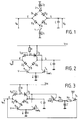
- FIG. 1 represents a conventional diagram of a sample and hold device. It has a diode bridge with two branches, one constituted by diodes D1 and D3 arranged directly and the other by diodes D2 and D4 also arranged directly.
- the point A common to the diodes D1 and D2 is connected to a current source I2 through a switching device 2.
- the point B common to the diodes D3 and D4 is connected to a current source I1 through a switching device 1.
- the point common to the diodes D1 and D3 constitutes the input E of the sampler which receives an input signal V e to be sampled.
- the point common to the diodes D2 and D4 constitutes the output S of the sampler. It is connected to a capacitor C which stores a voltage V s .
- V s copies the voltage Ve across the capacitor C.
- V e V s when the current in the capacitor C is zero, the diodes D1 and D2 being identical, as well as the diodes D3 and D4, and the sources current I1 and I2 delivering a current of the same value.
- the bridge In blocking mode, obtained by simultaneously opening the switching devices 1 and 2, the bridge has a high impedance state (infinite if the diodes are assumed to be perfect) and the previously sampled voltage Vs is stored in capacitor C.
- the circuit of FIG. 2 proposes an embodiment in which only a current source switches, which can be based on NPN transistors for better speed in the case of the usual methods.
- a resistor R is arranged instead of the current source I2 and the switching device 2.
- the diode D1 is produced in the form of an NPN transistor T1 whose base and collector are short-circuited and whose emitter is connected to input E.
- the diode D2 is replaced by a transistor NPN T2 whose emitter is connected to the output S and whose collector-base path is in parallel with the resistor R.
- the diode D1 could be produced otherwise but this embodiment best ensures the identity of the characteristics with the diode D2.
- a current source I is arranged to be switched either at the point common to the diodes D3 and D4 (point B) or at point A common to the bases of the transistors T1 and T2.
- An NPN type transistor T3 has its collector connected to point B and receives on its base a switching signal V.
- a NPN type T4 transistor also has its collector connected at point A, its emitter connected to that of transistor T3 and receives on its base a reference voltage V ref1 .
- the circuit of FIG. 3 proposes an improved circuit, which is provided with a compensation circuit which is added to the other elements, which are otherwise unmodified.
- the compensation circuit comprises two transistors T5 and T6 of NPN type, the emitters of which are possibly connected by two linearization resistors R2 and R3 in series, at the common point of which is connected a current source I ′.
- the base of transistor T5 is connected to input E and its collector is referenced to the supply voltage source V cc .
- the base of transistor T6 receives a reference voltage V ref2 and its collector is connected to point A.
- the function of this compensation circuit is to draw the excess part of the current which crosses the resistor R so as to maintain in the transistor T1 a constant current equal to I / 2 and thus ensuring equality of the currents in the two branches of the bridge whatever the input voltage V e .
- V B be the value of the minimum voltage to be sampled.
- V H be the value of the maximum voltage to be sampled.
- V CC - V BET 1 - V H R I 2 + I 6H
- FIG. 4 shows an embodiment in which transistors T7 and T8 mounted as a follower emitter and having current sources I7 and I8 connected to their respective emitters. These transistors are interposed between the bases of the transistors T5 and T6 and their output and delivering their respective input signals respectively Ve and V ref2 .
- the current source I is produced in such a way that the balance of the currents in the two branches and therefore the quality of the feedback does not depend on any variations, in particular as a function of the temperature, of the voltage d input nor of the value of the supply voltage V cc .
- This function is carried out by implementing transistors Q1 to Q4, T9 and T10 to obtain the desired law of variation for current I.
- the input voltage Ve is offset by a base-emitter voltage V be using a transistor T15 having in its emitter a current source I15.
- Current I is supplied by a transistor Q1 whose collector is connected to the coupled emitters of transistors T3 and T4 and whose emitter is connected to the common mode pole.
- the transistor Q1 forms a current mirror in a ratio k with a transistor Q2.
- the transistor Q2 has its base connected to that of the transistor Q1, its collector connected to the supply voltage V cc through a resistor R4 and its emitter connected to the common mode pole.
- a transistor T9 has its collector connected to the supply voltage V cc , its base at the collector of transistor Q2 and its emitter at the interconnected bases of transistors Q1 and Q2. The current passing through the collector of transistor Q2 then depends linearly on the value of resistance R4 (and on the supply voltage V cc ).
- a transistor Q3 has its collector connected to that of transistor Q2, its emitter at the common mode pole and has its base connected to that of transistor Q4 mounted as a diode by short-circuit base-collector with which it forms a second current mirror in a ratio N.
- a transistor T10 receives on its base the input signals V e , has its collector connected to the supply voltage source V cc and its emitter is connected to the base of the transistor Q4 through a resistor R10.
- K be the ratio between the emitter dimensions of the transistors Q1 and Q2, and N the ratio between the dimensions emitter of transistors Q3 and Q4.
- I Q1 , I Q2 , I Q3 , I Q4 , and I R4 be the currents in the collectors of the transistors Q1, Q2, Q3 and Q4 respectively, and across the resistor R4.
- I R4 V CC - 2V BE R4
- I Q4 V e - 2V BE R10
- I Q1 K ( V CC - 2V BE R4 - NOT Fr - 2V BE R10 )
- I Q1 K V CC R4 - KN R10 V e + 2KV BE (( NOT R10 - 1 R4 ) this expression must be identified in formula (4).
- the circuit shown in Figure 5 also includes means for improving the dynamic operation, ensuring the simultaneity of blocking the flow of current in the transistors T1 and T2 on the one hand and the diodes D3, D4 on the other. Blocking of transistors T1 and T2 occurs when the transistor T4 is crossed by the current I / 2. At this time, in fact, the potential at point A is equal to V cc - V e and all the current flowing through the resistor R passes through the transistor T4. On the other hand, the collector current of the transistor T3 continues transiently to pass through the diodes D3 and D4 until the transistor T3 is blocked.
- the current flowing through the diode D4 during this transient situation is supplied by the capacitor C which discharges slightly, which introduces a slight systematic error on the value of the stored voltage.
- a transistor T13 whose collector is connected to the supply voltage source V cc and its emitter at point B (point common to the cathode of diodes D3 and D4 and to the collector of transistor T3) has the function of supplying the collector with transistor T3 said transient current so as to ensure said simultaneous blocking and to avoid said transient discharge of capacitor C.
- its base is connected to a terminal of a series branch comprising a resistor R5 and a diode D5, the other terminal of the branch being connected to the source of supply voltage V cc .
- a transistor T15 whose emitter is connected to the input E of the bridge shifts the input signal level Ve by one V BE .
- a current source I15 force a constant current in its transmitter.
- the diodes D3 and D4 are Schottky diodes.
- the base of the transistor T13 is connected to the collector of a transistor T11 whose emitter is coupled to that of a transistor T12 whose collector is brought to the supply potential V cc .
- the bases of the transistors T11 and T12 receive the voltages respectively V ref1 and V, that is to say that its operation is simultaneous with that of the pair T3, T4.
- a current source (transistor Q5) is connected to the emitters of the transistors T11 and T12.
- the base of transistor Q5 is connected to that of transistor Q2, which means that these two transistors have their collector crossed by identical currents if they have the same dimension.
- the potential of the base of the transistor T13 increases, and this one can then supply the transistory current to the transistor T3.
- the diodes D3 and D4 being Schottky diodes (live V DS voltage ⁇ 0.5V), the voltage excursion on the collector of the transistor T11 is equal to (V BE - V DS ) ⁇ 0.3V to turn on the transistor T13.
- the diodes D3 and D4 are not necessarily Schottky diodes in the case where the dynamic correction assembly uses the transistor T13. It suffices in fact that, for example, the ratio of dimensions between the transistor T13 and the diodes D3 and D4 produced in this hypothesis from bipolar transistors is such that a negligible current flows through the transistor T13 when the bridge is conductive.
- the improvement of the dynamic operation is achievable with transistors of the same type as those implemented for the switching of the first switchable current source (in particular the second current source and the first differential stage.
Landscapes
- Electronic Switches (AREA)
- Amplifiers (AREA)
Claims (20)
- Schaltkreis mit einer Diodenbrücke, die eine erste Reihenschaltung aufweist mit einer ersten (T₁) und einer zweiten (D₃) Diode, die zu einer zweiten Reihenschaltung mit einer dritten (T₂) und einer vierten Diode (T₂) parallelgeschaltet sind, wobei ein erstes gemeinsames Ende (B) der obengenannten zwei Reihenschaltungen mit einer ersten schaltbaren Stromquelle verbunden ist, die einen ersten Zustand darstellt, in dem er mit dem ersten gemeinsamen Ende gekoppelt ist und einen zweiten Zustand, in dem er von dem ersten gemeinsamen Ende entkoppelt ist, wobei ein zweites gemeinsames Ende (A) der zwei genannten Zweige der gemeinsame Punkt der genannten ersten (T₁) und dritten Diode (T₂) ist, wobei die erste schaltbare Stromquelle dazu bestimmt ist mit dem zweiten gemeinsamen Ende (A) in dem Sperrzustand gekoppelt zu werden, wobei die erste Reihenschaltung eine Eingangsklemme (E) am gemeinsamen Verbindungspunkt der ersten (T₁) und der zwieten Diode (D₃) aufweist und dazu eingerichtet ist, eine Eingangsspannung zu empfangen, wobei die zweite Reihenschaltung eine Ausgangsklemme (5) aufweist am Verbindungspunkt der dritten (T₂) und der vierten Diode (D₄), dadurch gekennzeichnet, daß die dritte Diode durch die Basis-Emitter-Strecke eines ersten Transistors (T₂) gebildet ist, dessen Kollektor mit einer Speisespannungsquelle verbunden ist und daß der Schaltkreis einen ersten Widerstand (R) aufweist zwischen dem genannten zweiten gemeinsamen Ende (A) und der genannten Speisespannungsquelle (Vcc), wobei die zweite schaltbare Stromquelle dazu vorgesehen ist, mit dem zweiten gemeinsamen Ende (A) in zum Sperrzustand gekoppelt zu werden.
- Schaltkreis nach Anspruch 1, dadurch gekennzeichnet, daß die erste schaltbare Stromquelle eine erste differentielle Stufe (T₃, T₄) aufweist zum Schalten des Stromes (I) einer bestimmten Stärke zwischen dem genannten ersten und zweiten gemeinsamen Ende in dem Abtastzustand und in dem Sperrzustand, in Antwort auf ein Steuersignal (V).
- Schaltkreis nach Anspruch 2, dadurch gekennzeichnet, daß er einen Stromgeneratorkreis (T₅, T₆, R₂, R₃) aufweist zum Injektieren an dem genannten zweiten gemeinsamen Ende (A) eines Ausgleichstromes, variierend in Funktion der Eingangsspannung, damit ein Gleichgewicht der Brücke beibehalten wird, unabhängig von der genannten Eingangsspannung.
- Schaltkreis nach Anspruch 3, dadurch gekennzeichnet, daß der Stromgenerator eine zweite schaltbare differentielle Stufe ist, damit der genannte Ausgleichstrom von einer dritten Stromquelle erzeugt wird mit einer bestimmten Stärke (I′).
- Schaltkreis nach Anspruch 4, dadurch gekennzeichnet, daß die zweite differentuelle Stufe einen dritten (T₅) und einen vierten Transistor (T₆) aufweist, deren Emitter über einen zweiten (R₂) und einen dritten Widerstand (R₃) in Reihe geschaltet sind, mit deren gemeinsamem Punkt die dritte Stromquelle verbunden ist, wobei die Basis des dritten Transistors (T₅) dazu vorgesehen ist, die genannten Eingangsspannung zu erhalten und der Kollektor mit der Speisespannungsquelle verbunden ist, wobei die Basis des vierten Transistors (T₆) dazu vorgesehen ist, eine Bezugsspannung zu erhalten und der Kollektor mit dem gemeinsamen zweiten Ende (A) verbunden ist.
- Schaltkrteis nach Anspruch 5, dadurch gekennzeichnet, daß die Basis-Emitterstrecke des dritten (T₅) und des vierten (T₆) Transistors mit einer fünften (T₇) und einer sechsten Pgelabtastdiode (T₈) in Reihe geschaltet sind.
- Schaltkreis nach Anspruch 4 bis 6, dadurch gekennzeichnet, daß die dritte Stromquelle die nachfolgende Stärke hat:

 VH : maximaler Wert des Eingangssignals VeVB : minimaler Wert des Eingangssignals VeR : Wert des ersten TransistorsVBE : Basis-Emitter-Spannung eines TransistorsVCC : SpeisespannungI : Stärke der ersten Stromquelle mit einem bestimmten Wert.
 - Schaltkreis nach Anspruch 7, dadurch gekennzeichnet, daß der zweite (R₂) und der dritte Widerstand (R₃) denselben Wert haben, gleich:

- Schaltkreis nach Anspruch 2, dadurch gekennzeichnet, daß die erste Stromquelle derart vorgesehen ist, daß der Strom I nach einem bestimmten Gesetz variiert, und zwar:

Vcc die Speisespannung ist und
Ve die Eingangsspannung ist. - Schaltkreis nach Anspruch 9, dadurch gekennzeichnet, daß die erste Stromquelle in Stromspiegelschaltung vorgesehen ist in einem verhältnis K mit einer vierten Stromquelle (Q₂, Q₄), deren Stärke eine Funktion der Speisespannung ist, und die einen Teil des Stromes zu einer fünften Stromquelle (Q₃, Q₄, T₁₀, R₁₀) führt, deren Stärke eine Funktion der Eingangsspannung ist, derart, daß die Stärke der ersten Stromquelle dem genannten Gesetz folgt.
- Schaltkreis nach Anspruch 10, dadurch gekennzeichnet, daß die vierte Stromquelle einen vierten Widerstand (R₄) aufweist, dessen einer Anschluß mit der Speisespannungsquelle verbunden ist und dessen zweiter Anschluß mit der fünften Stromquelle (Q₃) verbunden ist, wobei der vierte Widerstand (R₄) derart vorgesehen ist, daß der Strom der vierten Stromquelle linear von dem Wert des vierten Widerstandes (R₄) abhängig ist.
- Schaltkreis nach Anspruch 11, dadurch gekennzeichnet, daß das verhältnis K zwischen der ersten und der vierten Stromquelle den nachfolgenden Wert hat:

- Schaltkreis nach einem der Ansprüche 10 bis 12, dadurch gekennzeichnet, daß die fünfte Stromquelle einerseits einen fünften Transistor (T₁₀) aufweist, dessen Basis vorgesehen ist zum Zuführen der genannten Eingangsspannung (Ve), dessen Kollektor mit der genannten Speisespannungsquelle verbunden ist und dessen Emitter in Reihe mit einem fünften Widerstand (R₁₀) und einer siebenten Gleichstromdiode (Q₄) und ebenfalls mit einem sechsten Transistor (Q₃) verbunden ist, dessen Kollektor mit dem zweiten Anschluß des vierten Widerstandes (R₄) verbunden ist zum Liefern des gewünschten Stromes, wobei der Verbindungspunkt des fünften Widerstandes (R₁₀) und der siebenten Diode (Q₄) mit der Basis des sechsten Transistors (Q₃) verbunden ist.
- Schaltkreis nach Anspruch 13, dadurch gekennzeichnet, daß die Abmessungen des sechsten Transistors und der siebenten Diode sind vorzugsweise derart, daß sie von Strömen durchlaufen werden mit einer Rate N, und daß:

- Schaltkreis nach Anspruch 14, dadurch gekennzeichnet, daß er einen zweiten Stromgenerator aufweist zum Eingeben eines Übergangsstromes zu dem genannten gemeinsamen Ende (B) während der Änderung aus dem Abtastzustand in den Haltezustand, zum Erzeugen des Übergangsstroms durch die erste differentielle Stufe.
- Schaltkreis nach Anspruch 15, dadurch gekennzeichnet, daß der zweite Stromgenerator einen siebenten Transistor (T₁₃) aufweist, dessen Kollektor mit der Speisespannungsquelle verbunden ist, dessen Emitter mit dem ersten gemeinsamen Ende (B) verbunden ist und dessen Basis mit der Speisespannungsquelle verbunden ist über eine achte Diode (D₅), die in Reihe mit einem sechsten Widerstand (R₅) und ebenfalls mit einer Ausgangsklemme eines dritten Schaltkreises verbunden ist, der vorgesehen ist zum Verbinden desselben mit einer sechsten Stromquelle (Q₅), deren Stärke zu der der vierten Stromquelle (Q₂) proportional ist, wenn die Änderung aus dem ersten in den zweiten Zustand durchgeführt wird.
- Schaltkreis nach Anspruch 16, dadurch gekennzeichnet, daß die zweite (D₃) und die vierte Diode (D₄) Schottky-Dioden sind.
- Schaltkreis nach Anspruch 16 oder 17, dadurch gekennzeichnet, daß die vierte und die sechste Stromquelle dieselbe Stärke haben und zwar:

- Schaltkreis nach Anspruch 15 bis 18, dadurch gekennzeichnet, daß die erste schaltbare Stromquelle und der zweite Stromerzeugerkreis Halbleiterelemente gleich Typs (NPN) aufweisen.
- Abtast-und-Halteschaltung, dadurch gekennzeichnet, daß sie einen Schaltkreis nach einem der vorstehenden Ansprüche aufweist und einen Speicherkondensator (C), der mit der genannten Ausgangsklemme verbunden ist, wobei der erste Zustand ein Abtastzustand ist und der zweite Zustand ein Sperrzustand ist.
Applications Claiming Priority (2)
| Application Number | Priority Date | Filing Date | Title |
|---|---|---|---|
| FR8908418 | 1989-06-23 | ||
| FR8908418A FR2648943B1 (fr) | 1989-06-23 | 1989-06-23 | Circuit echantillonneur-bloqueur |
Publications (2)
| Publication Number | Publication Date |
|---|---|
| EP0406930A1 EP0406930A1 (de) | 1991-01-09 |
| EP0406930B1 true EP0406930B1 (de) | 1995-02-01 |
Family
ID=9383081
Family Applications (1)
| Application Number | Title | Priority Date | Filing Date |
|---|---|---|---|
| EP90201577A Expired - Lifetime EP0406930B1 (de) | 1989-06-23 | 1990-06-18 | Schaltkreis, insbesondere als Abtast- und Haltkreis |
Country Status (5)
| Country | Link |
|---|---|
| US (1) | US5089720A (de) |
| EP (1) | EP0406930B1 (de) |
| JP (1) | JP2847149B2 (de) |
| DE (1) | DE69016519T2 (de) |
| FR (1) | FR2648943B1 (de) |
Families Citing this family (2)
| Publication number | Priority date | Publication date | Assignee | Title |
|---|---|---|---|---|
| JP3103154B2 (ja) * | 1990-10-30 | 2000-10-23 | 株式会社東芝 | サンプル・ホールド回路 |
| EP1172661B1 (de) * | 2001-03-10 | 2003-02-19 | Agilent Technologies, Inc. (a Delaware corporation) | Umschaltbare Testschaltung für asymmetrischen und differentiellen Abschluss |
Family Cites Families (8)
| Publication number | Priority date | Publication date | Assignee | Title |
|---|---|---|---|---|
| US3643110A (en) * | 1970-11-30 | 1972-02-15 | Motorola Inc | Sample and hold circuit |
| US3721829A (en) * | 1971-08-23 | 1973-03-20 | Bell Telephone Labor Inc | Autobalanced diode bridge sampling gate |
| JPS58115693A (ja) * | 1981-12-28 | 1983-07-09 | Sony Corp | サンプルホ−ルド回路 |
| US4518921A (en) * | 1982-10-18 | 1985-05-21 | At&T Bell Laboratories | Track and hold circuit |
| JPS60103596A (ja) * | 1983-11-11 | 1985-06-07 | Toshiba Corp | サンプル・ホ−ルド回路 |
| EP0213845A3 (de) * | 1985-08-30 | 1988-06-22 | Advanced Micro Devices, Inc. | Abtast- und Halteschaltung |
| US4728819A (en) * | 1986-08-27 | 1988-03-01 | Honeywell Inc. | Switching network |
| FR2604819B1 (fr) * | 1986-10-03 | 1988-12-09 | Thomson Semiconducteurs | Echantillonneur-bloqueur a haute frequence d'echantillonnage |
-
1989
- 1989-06-23 FR FR8908418A patent/FR2648943B1/fr not_active Expired - Fee Related
-
1990
- 1990-06-18 DE DE69016519T patent/DE69016519T2/de not_active Expired - Fee Related
- 1990-06-18 EP EP90201577A patent/EP0406930B1/de not_active Expired - Lifetime
- 1990-06-21 US US07/542,219 patent/US5089720A/en not_active Expired - Fee Related
- 1990-06-22 JP JP2162977A patent/JP2847149B2/ja not_active Expired - Lifetime
Also Published As
| Publication number | Publication date |
|---|---|
| DE69016519T2 (de) | 1995-08-31 |
| EP0406930A1 (de) | 1991-01-09 |
| FR2648943A1 (fr) | 1990-12-28 |
| JPH0363997A (ja) | 1991-03-19 |
| US5089720A (en) | 1992-02-18 |
| DE69016519D1 (de) | 1995-03-16 |
| JP2847149B2 (ja) | 1999-01-13 |
| FR2648943B1 (fr) | 1991-10-11 |
Similar Documents
| Publication | Publication Date | Title |
|---|---|---|
| EP0511707B1 (de) | Kaskodendifferenzverstärker | |
| EP0248473B1 (de) | Umsetzerschaltung mit drei logischen Zuständen | |
| JP3103154B2 (ja) | サンプル・ホールド回路 | |
| EP0845856A1 (de) | Rauscharmer Transkonduktanzverstärker mit hoher Aussteuerung | |
| JP4923308B2 (ja) | 追跡および保持増幅器 | |
| JPH0554689A (ja) | サンプルホールド回路およびバツフア回路およびそれらを用いたサンプルホールド装置 | |
| US4873457A (en) | Integrated sample and hold circuit | |
| EP0309366B1 (de) | Stromdifferenzverstärker mit sequentieller Wirkungsweise | |
| EP0406930A1 (de) | Schaltkreis, insbesondere als Abtast- und Haltkreis | |
| EP0200255B1 (de) | Schaltstufe einer Darlington-Type insbesondere für Speicher-Wortzeile-Dekodierer | |
| US10224113B2 (en) | Sampling device | |
| FR2834805A1 (fr) | Generateur de courant ou de tension ayant un point de fonctionnement stable en temperature | |
| US5315170A (en) | Track and hold circuit | |
| EP0816965A1 (de) | Temperaturabhängig geregelter Referenzspannungsgenerator | |
| EP0353808B1 (de) | Stromausgleichsschaltung | |
| EP0536063B1 (de) | Präzisionsstromgenerator | |
| EP0479377B1 (de) | Stromquelle mit bestimmtem Verhältnis zwischen Eingangs- und Ausgangsströmen | |
| FR2694850A1 (fr) | Etage amplificateur à faible distorsion thermique. | |
| EP0113975B2 (de) | Kontrollierbarer Ablenkgenerator | |
| JPS6031130B2 (ja) | サンプル・ホ−ルド回路 | |
| EP0242304B1 (de) | Folgeverstärker mit grosser Anstiegsgeschwindigkeit | |
| FR2741212A1 (fr) | Dispositif de limitation du courant de sortie d'un amplificateur operationnel | |
| FR2684205A1 (fr) | Miroir de courant a faible erreur de recopie. | |
| JP2541010B2 (ja) | サンプルホ―ルド回路 | |
| FR2755805A1 (fr) | Circuit d'amplification comprenant un dispositif de compensation de courant d'entree |
Legal Events
| Date | Code | Title | Description |
|---|---|---|---|
| PUAI | Public reference made under article 153(3) epc to a published international application that has entered the european phase |
Free format text: ORIGINAL CODE: 0009012 |
|
| AK | Designated contracting states |
Kind code of ref document: A1 Designated state(s): DE FR GB IT |
|
| 17P | Request for examination filed |
Effective date: 19910704 |
|
| RAP1 | Party data changed (applicant data changed or rights of an application transferred) |
Owner name: N.V. PHILIPS' GLOEILAMPENFABRIEKEN Owner name: PHILIPS COMPOSANTS |
|
| 17Q | First examination report despatched |
Effective date: 19940413 |
|
| GRAA | (expected) grant |
Free format text: ORIGINAL CODE: 0009210 |
|
| AK | Designated contracting states |
Kind code of ref document: B1 Designated state(s): DE FR GB IT |
|
| REF | Corresponds to: |
Ref document number: 69016519 Country of ref document: DE Date of ref document: 19950316 |
|
| ITF | It: translation for a ep patent filed | ||
| GBT | Gb: translation of ep patent filed (gb section 77(6)(a)/1977) |
Effective date: 19950420 |
|
| PLBE | No opposition filed within time limit |
Free format text: ORIGINAL CODE: 0009261 |
|
| STAA | Information on the status of an ep patent application or granted ep patent |
Free format text: STATUS: NO OPPOSITION FILED WITHIN TIME LIMIT |
|
| 26N | No opposition filed | ||
| REG | Reference to a national code |
Ref country code: FR Ref legal event code: CD |
|
| PGFP | Annual fee paid to national office [announced via postgrant information from national office to epo] |
Ref country code: DE Payment date: 19980824 Year of fee payment: 9 |
|
| PGFP | Annual fee paid to national office [announced via postgrant information from national office to epo] |
Ref country code: GB Payment date: 19990621 Year of fee payment: 10 |
|
| PGFP | Annual fee paid to national office [announced via postgrant information from national office to epo] |
Ref country code: FR Payment date: 19990628 Year of fee payment: 10 |
|
| REG | Reference to a national code |
Ref country code: FR Ref legal event code: TP |
|
| PG25 | Lapsed in a contracting state [announced via postgrant information from national office to epo] |
Ref country code: DE Free format text: LAPSE BECAUSE OF NON-PAYMENT OF DUE FEES Effective date: 20000503 |
|
| PG25 | Lapsed in a contracting state [announced via postgrant information from national office to epo] |
Ref country code: GB Free format text: LAPSE BECAUSE OF NON-PAYMENT OF DUE FEES Effective date: 20000618 |
|
| GBPC | Gb: european patent ceased through non-payment of renewal fee |
Effective date: 20000618 |
|
| PG25 | Lapsed in a contracting state [announced via postgrant information from national office to epo] |
Ref country code: FR Free format text: LAPSE BECAUSE OF NON-PAYMENT OF DUE FEES Effective date: 20010228 |
|
| REG | Reference to a national code |
Ref country code: FR Ref legal event code: ST |
|
| PG25 | Lapsed in a contracting state [announced via postgrant information from national office to epo] |
Ref country code: IT Free format text: LAPSE BECAUSE OF NON-PAYMENT OF DUE FEES;WARNING: LAPSES OF ITALIAN PATENTS WITH EFFECTIVE DATE BEFORE 2007 MAY HAVE OCCURRED AT ANY TIME BEFORE 2007. THE CORRECT EFFECTIVE DATE MAY BE DIFFERENT FROM THE ONE RECORDED. Effective date: 20050618 |