EP0405573A2 - Bilderzeugungsgerät - Google Patents
Bilderzeugungsgerät Download PDFInfo
- Publication number
- EP0405573A2 EP0405573A2 EP90112449A EP90112449A EP0405573A2 EP 0405573 A2 EP0405573 A2 EP 0405573A2 EP 90112449 A EP90112449 A EP 90112449A EP 90112449 A EP90112449 A EP 90112449A EP 0405573 A2 EP0405573 A2 EP 0405573A2
- Authority
- EP
- European Patent Office
- Prior art keywords
- recording medium
- developer
- removing means
- recording
- detecting
- Prior art date
- Legal status (The legal status is an assumption and is not a legal conclusion. Google has not performed a legal analysis and makes no representation as to the accuracy of the status listed.)
- Granted
Links
Images


Classifications
-
- G—PHYSICS
- G03—PHOTOGRAPHY; CINEMATOGRAPHY; ANALOGOUS TECHNIQUES USING WAVES OTHER THAN OPTICAL WAVES; ELECTROGRAPHY; HOLOGRAPHY
- G03G—ELECTROGRAPHY; ELECTROPHOTOGRAPHY; MAGNETOGRAPHY
- G03G21/00—Arrangements not provided for by groups G03G13/00 - G03G19/00, e.g. cleaning, elimination of residual charge
- G03G21/0005—Arrangements not provided for by groups G03G13/00 - G03G19/00, e.g. cleaning, elimination of residual charge for removing solid developer or debris from the electrographic recording medium
- G03G21/0035—Arrangements not provided for by groups G03G13/00 - G03G19/00, e.g. cleaning, elimination of residual charge for removing solid developer or debris from the electrographic recording medium using a brush; Details of cleaning brushes, e.g. fibre density
-
- G—PHYSICS
- G03—PHOTOGRAPHY; CINEMATOGRAPHY; ANALOGOUS TECHNIQUES USING WAVES OTHER THAN OPTICAL WAVES; ELECTROGRAPHY; HOLOGRAPHY
- G03G—ELECTROGRAPHY; ELECTROPHOTOGRAPHY; MAGNETOGRAPHY
- G03G15/00—Apparatus for electrographic processes using a charge pattern
- G03G15/22—Apparatus for electrographic processes using a charge pattern involving the combination of more than one step according to groups G03G13/02 - G03G13/20
- G03G15/34—Apparatus for electrographic processes using a charge pattern involving the combination of more than one step according to groups G03G13/02 - G03G13/20 in which the powder image is formed directly on the recording material, e.g. by using a liquid toner
- G03G15/344—Apparatus for electrographic processes using a charge pattern involving the combination of more than one step according to groups G03G13/02 - G03G13/20 in which the powder image is formed directly on the recording material, e.g. by using a liquid toner by selectively transferring the powder to the recording medium, e.g. by using a LED array
- G03G15/348—Apparatus for electrographic processes using a charge pattern involving the combination of more than one step according to groups G03G13/02 - G03G13/20 in which the powder image is formed directly on the recording material, e.g. by using a liquid toner by selectively transferring the powder to the recording medium, e.g. by using a LED array using a stylus or a multi-styli array
-
- G—PHYSICS
- G03—PHOTOGRAPHY; CINEMATOGRAPHY; ANALOGOUS TECHNIQUES USING WAVES OTHER THAN OPTICAL WAVES; ELECTROGRAPHY; HOLOGRAPHY
- G03G—ELECTROGRAPHY; ELECTROPHOTOGRAPHY; MAGNETOGRAPHY
- G03G2217/00—Details of electrographic processes using patterns other than charge patterns
- G03G2217/0008—Process where toner image is produced by controlling which part of the toner should move to the image- carrying member
- G03G2217/0016—Process where toner image is produced by controlling which part of the toner should move to the image- carrying member where the toner is conveyed over the electrode array to get a charging and then being moved
Definitions
- the present invention relates to an image forming apparatus wherein a developer is deposited on a recording medium, more particularly to an apparatus wherein an electric charge is applied on the recording medium by a recording electrode; the developer is deposited electrostatically on the charge; and the developer is removed from the recording medium thereafter.
- U.S. Patent No. 3,914,771 Japanese Patent Application Publication No. 46707/1976 or the like discloses an image forming method wherein the developer is deposited on the recording medium.
- conductive and magnetic toner 1 having a volume resistivity of 103 - 1010 ohm.cm is carried on a non-magnetic cylinder 3 with the aid of a rotating magnet 2, and the toner is passed on the recording electrode 4 made of magnetic material.
- a recording medium 5 has a conductive layer 7 and a surface insulating layer having a thickness of 1 - 10 micron and a volume resistivity of 108 - 1015 ohm.cm.
- a voltage is applied between the conductive layer 7 and the recording electrode 4, by which the toner 1 is deposited on the recording medium 5 to form an image.
- FIG. 3 shows an example of such an image forming apparatus functioning as a display apparatus.
- the reference numeral 1 designates the toner.
- the apparatus comprises a recording electrode 4, the recording material (recording medium) 5 in the form of an endless belt, which will hereinafter be called "a recording belt”, an erasing member 8 for removing the toner to erase the image, a toner container 10, recording belt supporting rollers 11, a main frame 12 and a record controller 13.
- the toner 1 is selectively deposited on the recording belt 5 to form an image.
- a signal voltage of 40 V is applied from the record controller 13
- the toner 1 is electrostatically deposited on the recording belt 5, whereas when 0 V is applied, the toner is attracted by the magnetic force so as not to be deposited on the recording medium. In this manner, an image is formed.
- the recording belt supporting roller 11 is driven by an unshown motor so that the recording belt 5 is rotated in the direction indicated by an arrow to present the image by the toner 1 to a display position where the image is displayed.
- the toner image is contacted to an erasing member 8 made of electrically conductive carbon fibers, conductive resin, conductive rubber or the like having a volume resistivity of 101 - 106 ohm.cm approximately, by which the electrostatic charge is removed from the recording belt 5, and the toner is mechanically removed from the recording medium.
- the toner 1 falls by the weight thereof into the container 10, and is prepared for the next recording operation.
- the erasing member 8 is supplied with a predetermined voltage V for the toner removal. The voltage is determined on the basis of the triboelectric charge properties of the recording medium 5 and the erasing member 8.
- the image with insignificant fog can be provided with the application of -3 V, where the recording medium 5 is made of titanium oxide, and the erasing member is made of carbon fibers.
- Figure 4 shows the structure around the above-described erasing member 8.
- the recording medium 5 having the insulating layer 6 and the conductive layer 7 is conveyed by an unshown driving means downwardly (the direction indicated by the arrow). Since the erasing member 8 is supplied with a bias voltage of -3 V from the voltage source 14, the positive electrostatic charge on the insulating layer 6 is removed, by which the toner 1 having been electrostatically deposited on the recording medium 5 by the recording electrode 4 becomes easily removed. With the easy removal state established, the toner 1 is forcedly removed by the brush 8a made of conductive carbon fibers having the volume resistivity of 101 - 102 ohm.cm, from the recording medium 5. However, as will be understood from the Figure, the toner 1 remains in many cases even after the recording medium 5 passes by the erasing member 8.
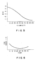
- Figure 5 shows the bias voltage relative to the relative humidity not producing the fog at 25 °C. However, if the temperature is changed with the relative humidity remaining unchanged, the foggy background is produced when the temperature is low or high, as shown in Figure 6.
- an image forming apparatus wherein the quantity of electricity on the toner removing member moving relative to the recording medium is detected, and in response to the detection, the bias voltage to be applied to the removing member is controlled, prior to the start of the image forming opereation.
- the triboelectric charge resulting from the rubbing between the removing member and the recording medium can be controlled, so that the fog production can be suppressed.
- the sharp image without fog can be provided even if the recording medium or the erasing member is deteriorated with use, or even if the electrostatic property of the toner changes by the contamination thereof with the foreign matter.
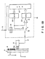
- FIG. 1A there is shown an image display apparatus to which the present invention is applicable.
- the same reference numerals as in the description hereinbefore are assigned to the corresponding elements, so that the detailed descriptions thereof are omitted for simplicity.
- the apparatus comprises a control instruction line 15 connected with a control circuit not shown, and detecting and control means 16 which is a major part of the present invention.
- a cable 17 electrically connects the detecting and control means 16 and the erasing means 8.
- Figure 1B illustrates the detecting and control means 16 in detail. It comprises a relay contact 18 and is switched to the side of contact a when a relay coil 19 is energized.
- a digital-analog converter 20 has an output which is connected to a contact b of the relay.
- An operational amplifier 21 produces an output to an analog-digital converter 22.
- a microcomputer 23 is supplied with an input thereto through the control instruction line 15 and is supplied with an output of the analog-digital converter 22. It supplies data to the digital-analog converter 20.
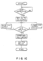
- Figure 1C shows a flow chart illustrating the sequential operation controlled by the microcomputer 23. The description will be made as to the operation of the circuit of Figure 1B along the flow chart of Figure 1C.
- an instruction signal is supplied to the detecting and control means 16 from an unshown control circuit through the control instruction line 15. Then, a control circuit (CPU) 23 detects the supply of the control signal, and supplies data to the digital-analog converter 20 to produce an output of -3 V. On the other hand, the recording medium 5 is conveyed at a constant speed predetermined by an unshown driving means.
- a control circuit (CPU) 23 detects the supply of the control signal, and supplies data to the digital-analog converter 20 to produce an output of -3 V.
- the recording medium 5 is conveyed at a constant speed predetermined by an unshown driving means.
- the output of the digital-analog converter 20 is fixed at -3 V. If the ambient condition is low temperature and low humidity, a voltage lower than -3 V is produced on the erasing member 8, as will be understood from Figures 5 and 6. If, for example, the voltage is -5 V, the output of the operational amplifier 21 has a positive polarity because the non-inversion input terminal of the operational amplifier 21 is supplied with -3 V, and because the inverse input terminal is supplied with -5 V.
- the analog-digital converter 22 converts the analog output of the operational amplifier 21 to digital data, which are supplied to the CPU 23.
- the CPU 23 discriminates whether it is positive or negative. In this example, it is positive, and therefore, the control is effected to lower the output of the digital-analog converter.
- the correction voltage is added upon the transient condition of the recording sheet speed, that is, before the regular speed thereof is not reached at the time of the start. More particularly, when the speed is lower than the regular speed, the detection tends to be lower. Therefore, the correction voltage is applied so that the applied voltage is the one which is obtained by dividing the voltage directly corresponding to detected voltage by the speed reduction ratio. When the speed thereof is higher than the regular speed, which may also occur at the time of the start, the correction voltage is added in the opposite direction. The correction may also be made on the basis of the integrated use period of the sheet or toner in terms of their service life.
- the amount of electric charge of the toner erasing means 8 is directly detected, and a voltage corresponding thereto is applied to the erasing means, by which the production of the fog by the electric charge remaining due to the recording operation and the triboelectric charge by the friction can be eliminated.
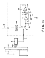
- Figure 1D shows a second embodiment.
- reference numerals 24 and 26 designate a resistor and a capacitor.
- the voltage is converted.
- the voltage is amplified by the operational amplifier 21.
- the voltage is peak-held by the capacitor 26 and the diode 30.
- the held voltage is properly amplified by a correcting circuit constituted by an operational amplifier 29, a resistor 25 and a resistor 27, and the resultant voltage is applied to the erasing means.
- the maximum of the electric charge produced on the erasing means 8 is applied to the erasing means.
- Figure 1E shows a further embodiment.
- the electric charge produced on the erasing member 8 is used to charge a capacitor, and the voltage produced by the capacitor is applied to the erasing member.
- the total amount of the electric charge in the period in which the relay 19 is energized appears on the control instruction line 15 connected to the unshown control circuit, and therefore, the good image without fog can be produced.
- the quantity of electricity in the removing member is detected, and the voltage corresponding thereto is applied to the removing member, and therefore, the good image without fog and with small remaining electric charge can be produced.
- the present invention is applied to another type of image forming apparatus such as a printer or a copying machine using an image formation mechanism shown in Figure 2.
- An image forming apparatus includes recording electrodes electrically isolated from each other, a recording medium movable relative to the recording electrodes and a developer supplying device for supplying a conductive developer into between the recording electrodes and the recording medium.
- the invention is particularly related to the removal of the developer from the recording medium. The amount of electricity produced in the means for removing the developer is detected, and in response to the detection, a bias voltage applied to the removing means is controlled.
Landscapes
- Physics & Mathematics (AREA)
- General Physics & Mathematics (AREA)
- Control Or Security For Electrophotography (AREA)
- Discharging, Photosensitive Material Shape In Electrophotography (AREA)
- Cleaning In Electrography (AREA)
- Printers Or Recording Devices Using Electromagnetic And Radiation Means (AREA)
Applications Claiming Priority (2)
| Application Number | Priority Date | Filing Date | Title |
|---|---|---|---|
| JP1169408A JP2714154B2 (ja) | 1989-06-30 | 1989-06-30 | 画像形成装置 |
| JP169408/89 | 1989-06-30 |
Publications (3)
| Publication Number | Publication Date |
|---|---|
| EP0405573A2 true EP0405573A2 (de) | 1991-01-02 |
| EP0405573A3 EP0405573A3 (en) | 1991-05-02 |
| EP0405573B1 EP0405573B1 (de) | 1994-08-31 |
Family
ID=15886046
Family Applications (1)
| Application Number | Title | Priority Date | Filing Date |
|---|---|---|---|
| EP90112449A Expired - Lifetime EP0405573B1 (de) | 1989-06-30 | 1990-06-29 | Bilderzeugungsgerät |
Country Status (4)
| Country | Link |
|---|---|
| US (1) | US5089832A (de) |
| EP (1) | EP0405573B1 (de) |
| JP (1) | JP2714154B2 (de) |
| DE (1) | DE69011993T2 (de) |
Families Citing this family (3)
| Publication number | Priority date | Publication date | Assignee | Title |
|---|---|---|---|---|
| EP0501793B1 (de) * | 1991-02-28 | 1997-06-18 | Canon Kabushiki Kaisha | Bilderzeugungsgerät mit verschiedenen Tönen |
| US5243350A (en) * | 1991-11-06 | 1993-09-07 | Grumman Aerospace Corporation | Optical control of TR modules |
| US5754193A (en) * | 1995-01-09 | 1998-05-19 | Xerox Corporation | Thermal ink jet printhead with reduced power bus voltage drop differential |
Family Cites Families (6)
| Publication number | Priority date | Publication date | Assignee | Title |
|---|---|---|---|---|
| US3914771A (en) * | 1973-11-14 | 1975-10-21 | Minnesota Mining & Mfg | Electrographic recording process and apparatus employing synchronized recording pulses |
| JPS5146707A (ja) * | 1974-10-21 | 1976-04-21 | Hisao Nagae | Nanjakujibanchuniuchikondakeeshinguchukunosunao oogaasukuriunitekyoryokuoshidashiteatsumitsusareta sunadenininokuikeiotsukurukoho oyobi sochi* |
| US4788564A (en) * | 1986-07-10 | 1988-11-29 | Canon Kabushiki Kaisha | Board recording apparatus with reduced smudge |
| JPH0719106B2 (ja) * | 1987-11-17 | 1995-03-06 | キヤノン株式会社 | 画像記録装置 |
| JPH06104368B2 (ja) * | 1988-04-23 | 1994-12-21 | キヤノン株式会社 | 静電画像形成装置 |
| US4937633A (en) * | 1989-07-21 | 1990-06-26 | Xerox Corporation | Cleaning blade defect sensing arrangement |
-
1989
- 1989-06-30 JP JP1169408A patent/JP2714154B2/ja not_active Expired - Fee Related
-
1990
- 1990-06-29 US US07/545,645 patent/US5089832A/en not_active Expired - Lifetime
- 1990-06-29 DE DE69011993T patent/DE69011993T2/de not_active Expired - Fee Related
- 1990-06-29 EP EP90112449A patent/EP0405573B1/de not_active Expired - Lifetime
Also Published As
| Publication number | Publication date |
|---|---|
| JPH0333884A (ja) | 1991-02-14 |
| EP0405573A3 (en) | 1991-05-02 |
| JP2714154B2 (ja) | 1998-02-16 |
| EP0405573B1 (de) | 1994-08-31 |
| DE69011993D1 (de) | 1994-10-06 |
| US5089832A (en) | 1992-02-18 |
| DE69011993T2 (de) | 1995-01-05 |
Similar Documents
| Publication | Publication Date | Title |
|---|---|---|
| KR930010873B1 (ko) | 이미지 형성장치 | |
| EP0367245A2 (de) | Bilderzeugungsgerät | |
| US4506975A (en) | Cleaning device | |
| JPH11153900A (ja) | 画像形成装置 | |
| EP0751440B1 (de) | Bilderzeugungsgerät | |
| JP3093422B2 (ja) | ブラシクリーニング装置 | |
| EP1422578A1 (de) | Bilderzeugungsgerät mit einem Strommesssystem in der Entwicklungsvorrichtung | |
| JP3131286B2 (ja) | 電子写真プリンタ | |
| US5089832A (en) | Image forming apparatus | |
| JPH08286475A (ja) | 現像装置 | |
| JP2872121B2 (ja) | 画像形成装置と転写方法 | |
| US4811045A (en) | Electrostatic image forming apparatus | |
| JPH09185219A (ja) | 帯電装置及び画像形成装置 | |
| JPH1195530A (ja) | 電子写真記録装置 | |
| JP3515861B2 (ja) | 画像形成装置 | |
| US5077566A (en) | Image forming apparatus | |
| JPH0822170A (ja) | 画像形成装置及びその帯電方法 | |
| JPH10198131A (ja) | 帯電装置および画像形成装置 | |
| JPH06202446A (ja) | 画像形成装置 | |
| JP2863201B2 (ja) | 現像装置 | |
| JPH0683179A (ja) | 電子写真装置 | |
| JPH08234545A (ja) | 帯電装置 | |
| JPH08334981A (ja) | 画像形成装置 | |
| JPH0333883A (ja) | 画像形成装置 | |
| JPH10207187A (ja) | 画像形成装置 |
Legal Events
| Date | Code | Title | Description |
|---|---|---|---|
| PUAI | Public reference made under article 153(3) epc to a published international application that has entered the european phase |
Free format text: ORIGINAL CODE: 0009012 |
|
| 17P | Request for examination filed |
Effective date: 19900629 |
|
| AK | Designated contracting states |
Kind code of ref document: A2 Designated state(s): DE FR GB IT |
|
| PUAL | Search report despatched |
Free format text: ORIGINAL CODE: 0009013 |
|
| AK | Designated contracting states |
Kind code of ref document: A3 Designated state(s): DE FR GB IT |
|
| 17Q | First examination report despatched |
Effective date: 19920910 |
|
| GRAA | (expected) grant |
Free format text: ORIGINAL CODE: 0009210 |
|
| AK | Designated contracting states |
Kind code of ref document: B1 Designated state(s): DE FR GB IT |
|
| PG25 | Lapsed in a contracting state [announced via postgrant information from national office to epo] |
Ref country code: IT Free format text: LAPSE BECAUSE OF FAILURE TO SUBMIT A TRANSLATION OF THE DESCRIPTION OR TO PAY THE FEE WITHIN THE PRE;WARNING: LAPSES OF ITALIAN PATENTS WITH EFFECTIVE DATE BEFORE 2007 MAY HAVE OCCURRED AT ANY TIME BEFORE 2007. THE CORRECT EFFECTIVE DATE MAY BE DIFFERENT FROM THE ONE RECORDED.SCRIBED TIME-LIMIT Effective date: 19940831 Ref country code: FR Effective date: 19940831 |
|
| REF | Corresponds to: |
Ref document number: 69011993 Country of ref document: DE Date of ref document: 19941006 |
|
| EN | Fr: translation not filed | ||
| PLBE | No opposition filed within time limit |
Free format text: ORIGINAL CODE: 0009261 |
|
| STAA | Information on the status of an ep patent application or granted ep patent |
Free format text: STATUS: NO OPPOSITION FILED WITHIN TIME LIMIT |
|
| 26N | No opposition filed | ||
| REG | Reference to a national code |
Ref country code: GB Ref legal event code: IF02 |
|
| PGFP | Annual fee paid to national office [announced via postgrant information from national office to epo] |
Ref country code: GB Payment date: 20040623 Year of fee payment: 15 |
|
| PGFP | Annual fee paid to national office [announced via postgrant information from national office to epo] |
Ref country code: DE Payment date: 20040708 Year of fee payment: 15 |
|
| PG25 | Lapsed in a contracting state [announced via postgrant information from national office to epo] |
Ref country code: GB Free format text: LAPSE BECAUSE OF NON-PAYMENT OF DUE FEES Effective date: 20050629 |
|
| PG25 | Lapsed in a contracting state [announced via postgrant information from national office to epo] |
Ref country code: DE Free format text: LAPSE BECAUSE OF NON-PAYMENT OF DUE FEES Effective date: 20060103 |
|
| GBPC | Gb: european patent ceased through non-payment of renewal fee |
Effective date: 20050629 |