EP0404012A2 - Einrichtung zum Zugriff auf Vektordaten - Google Patents
Einrichtung zum Zugriff auf Vektordaten Download PDFInfo
- Publication number
- EP0404012A2 EP0404012A2 EP90111448A EP90111448A EP0404012A2 EP 0404012 A2 EP0404012 A2 EP 0404012A2 EP 90111448 A EP90111448 A EP 90111448A EP 90111448 A EP90111448 A EP 90111448A EP 0404012 A2 EP0404012 A2 EP 0404012A2
- Authority
- EP
- European Patent Office
- Prior art keywords
- data
- register
- element number
- vector data
- selection signal
- Prior art date
- Legal status (The legal status is an assumption and is not a legal conclusion. Google has not performed a legal analysis and makes no representation as to the accuracy of the status listed.)
- Granted
Links
Images


Classifications
-
- G—PHYSICS
- G06—COMPUTING OR CALCULATING; COUNTING
- G06F—ELECTRIC DIGITAL DATA PROCESSING
- G06F9/00—Arrangements for program control, e.g. control units
- G06F9/06—Arrangements for program control, e.g. control units using stored programs, i.e. using an internal store of processing equipment to receive or retain programs
- G06F9/30—Arrangements for executing machine instructions, e.g. instruction decode
- G06F9/30003—Arrangements for executing specific machine instructions
- G06F9/30007—Arrangements for executing specific machine instructions to perform operations on data operands
- G06F9/30021—Compare instructions, e.g. Greater-Than, Equal-To, MINMAX
-
- G—PHYSICS
- G06—COMPUTING OR CALCULATING; COUNTING
- G06F—ELECTRIC DIGITAL DATA PROCESSING
- G06F7/00—Methods or arrangements for processing data by operating upon the order or content of the data handled
-
- G—PHYSICS
- G06—COMPUTING OR CALCULATING; COUNTING
- G06F—ELECTRIC DIGITAL DATA PROCESSING
- G06F7/00—Methods or arrangements for processing data by operating upon the order or content of the data handled
- G06F7/22—Arrangements for sorting or merging computer data on continuous record carriers, e.g. tape, drum, disc
-
- G—PHYSICS
- G06—COMPUTING OR CALCULATING; COUNTING
- G06F—ELECTRIC DIGITAL DATA PROCESSING
- G06F9/00—Arrangements for program control, e.g. control units
- G06F9/06—Arrangements for program control, e.g. control units using stored programs, i.e. using an internal store of processing equipment to receive or retain programs
- G06F9/30—Arrangements for executing machine instructions, e.g. instruction decode
- G06F9/30003—Arrangements for executing specific machine instructions
- G06F9/30007—Arrangements for executing specific machine instructions to perform operations on data operands
- G06F9/30036—Instructions to perform operations on packed data, e.g. vector, tile or matrix operations
Definitions
- the present invention relates to retrieval of maximum and minimum values of vector data and, more particularly, to a vector data retrieval apparatus capable of retrieving element numbers corresponding to maximum or minimum values as retrieval results together with data.
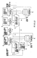
- Fig. 3 shows a conventional vector data retrieval apparatus.
- reference numeral 1 denotes a vector data holding means for holding an ordered set of vector data; 2, a register in which vector data read out from the vector data holding means 1 is set; 3, an element number generating means for generating an element number corresponding to the vector data; 4, a register in which the element number generated by the element number generating means 3 is set; 5, a comparing means for comparing the data stored in the register 2 with data stored in a register 8 (to be described below) and outputting a selection signal T0; 6, a selecting means for selecting one of vector data F1 and F2 respectively stored in the registers 2 and 8 in response to the selection signal T0; 7, a selecting means for selecting one of element numbers G1 and G2 respectively stored in the register 4 and a register 9 (to be described below) in response to the selection signal T0; 8, the register for storing vector data selected by the selecting means 6; and 9, the register for storing an element number selected by the selecting means 7.
- the first data of an ordered set of vector data is output from the vector holding means 1 and is set in the register 2.
- An element number corresponding to the vector data is generated by the element number generating means 3 and is set in the register 4.
- the data comparing means 5 compares the vector data stored in the register 2 with vector data stored in the register 8. In this case, however, since no vector data is stored in the register 8, the data comparing means 5 does not perform data comparison but generates a selection signal T0 for causing the selection means 6 and 7 to select the data stored in the registers 2 and 4, respectively.
- the second data held in the vector data holding means 1 is output and set in the register 2.
- An element number corresponding to this vector data is generated by the element number generating means and is set in the register 4.
- the previous data in the registers 2 and 4 i.e., the first data of the ordered set of vector data and the corresponding element numbers, are respectively stored in the registers 8 and 9 in accordance with the selection signal T0, which is generated by the data comparing means 5 in the first cycle to cause the selecting means 6 and 7 to select the data.
- the data comparing means 5 compares values F1 and F2 of the vector data respectively stored in the registers 2 and 8, i.e., the second and first data of the vector data, with each other.
- the data comparing means 5 then generates and outputs a selection signal T0 for causing the selecting means 6 to select a larger value in response to an instruction of "maximum value retrieval” and to select a smaller value in response to an instruction of "minimum value retrieval". If the value of the vector data stored in the register 2 is equal to that of the vector data stored in the register 8, the data comparing means 5 always generates and outputs a selection signal T0 for causing the selecting means 6 to select the value set in the register 8. More specifically, the comparing means 5 receives the data F1 and F2 as comparison targets and generates the signal T0 for causing the selecting means 6 to select the data F1 if the instruction of "maximum value retrieval" is provided and F1 > F2.
- the comparing means 5 If the instruction of "maximum value retrieval" is provided and F1 ⁇ F2, the comparing means 5 generates the signal T0 for causing the selection means 6 to select the data F2. The comparing means 5 generates the signal T0 for causing the selecting means 6 to select the data F1 if the instruction of "minimum value retrieval” is provided and F1 ⁇ F2. If the instruction of "minimum value retrieval” is provided and F1 ⁇ F2, the comparing means 5 generates the signal T0 for causing the selection means 6 to select the data F2.
- the selection means 7 selects and outputs either an output G2 from the register 9, in which the element number corresponding to the first data of the vector data is stored, or an output G1 from the register 4, in which the element number corresponding to the second data of the vector data is stored, in accordance with the same selection signal T0 as supplied to the selecting means 6.
- the maximum or minimum values of n vector data ( n is a natural number) can be stored in the register 8 in the (n+1)th cycle time, and an element number corresponding to the maximum or minimum value stored in the register 8 can be stored in the register 9.
- the vector data must be rearranged to be input to the vector data retrieval apparatus in an order of increasing element numbers. If the largest element number is required, the vector data must be rearranged to be input to the vector data retrieval apparatus in an order of decreasing element numbers. This undesirably increases the processing time as a whole.
- a vector data retrieval apparatus for receiving an ordered set of vector data and retrieving/outputting a maximum or minimum value of the vector data and an element number corresponding to the maximum or minimum value, comprising means for instructing whether to output a smallest or largest element number of element numbers to be output when a plurality of maximum or minimum values are present in the vector data.
- an instruction can be provided to designate whether to output the largest or smallest element number of element numbers to be output, as needed.
- Fig. 1 shows a vector data retrieval apparatus according to an embodiment of the present invention.
- reference numeral 10 denotes a selecting means for selecting either an output D1 from a register 2 or an output D2 from a register 8 in accordance with a selection signal S0, and outputting it to the register 8; 11, a selecting means for selecting either an output E1 from a register 4 or an output E2 from a register 9, and outputting it to the register 9; 12, an element number comparing means for comparing the output E1 from the register 4 with the output E2 from the register 9, i.e., the value of an element number corresponding to the second vector data of the vector data with the value of an element number corresponding to the first vector data so as to obtain a relationship in magnitude, and generating and outputting a comparison data signal S2 representing it; and 13, a selection signal generating means.
- the selection signal generating means 13 compares an output S1 from the data comparing means 5 with an output S2 from the element number comparing means 12, and performs the following
- the selection signal generating means 13 In a case wherein the values of data as comparison targets are not equal in value, the selection signal generating means 13 generates and outputs the output E1 from the register 4 when the selecting means 10 selects an element number corresponding to data to be selected, i.e., the output D1 from the register 2. When the selecting means 10 selects the output D2 from the register 8, the selection signal generating means 13 generates and outputs a selection signal S3 for selecting the output E2 from the register 9.
- the first data of an ordered set of vector data is output from the vector holding means 1 and is set in the register 2.
- An element number corresponding to this vector data is generated by the element number generating means 3 and is set in the register 4.
- the data comparing means 5 compares the vector data stored in the register 2 with vector data stored in the register 8. In this case, since no vector data is stored in the register 8, no data comparison is performed, and the selecting means 10 generates and outputs a selection signal S0 for selecting the output D1 from the register 2.
- Values stored in the registers 4 and 9 are element numbers to be compared by the element number comparing means 12.
- the element number comparing means 12 since no element number as a comparison target is stored in the register 9, the element number comparing means 12 does not perform comparison but commands the selection signal generating means 13 to generate a selection signal S3 for causing the selecting means 11 to select the output E1 from the register 4.
- the second data held in the vector data holding means 1 is read out and set in the register 2.
- an element number corresponding to the second data is set in the register 4.
- the output D1 (the first vector data) is set in the register 8
- the output E1 (the first element number corresponding to the first vector data) from the register 4 is set in the register 9.
- the data comparing means 5 compares the output D1 from the register 2 with the output D2 from the register 8, i.e., the second data of the vector data with the first data.
- the comparing means 5 then generates a selection signal S0 for causing the selecting means 10 to select a larger value in response to an instruction of "maximum value retrieval", and to select a smaller value in response to an instruction of "minimum value retrieval". If the data stored in the registers 2 and 8 are equal in value, the comparing means 5 always generates and outputs a selection signal S0 for causing the selecting means 10 to select the output D1 from the register 2.
- the selecting means 10 selects one of the outputs D1 and D2 from the registers 2 and 8 in accordance with this selection signal S0, and outputs it to the register 8.
- the data comparing means 5 outputs, to the selection signal generating means 13, a signal S1 representing whether the outputs D1 and D2 from the registers 2 and 8 are equal in value, together with the signal for designating the selecting means 10 to select one of the outputs D1 and D2 from the registers 2 and 8.
- the element number comparing means 12 compares the output E1 from the register 4 with the output E2 from the register 9, i.e., the value of the element number corresponding to the second data of the vector data with the value of the element number corresponding to the first data so as to obtain a relationship in magnitude, and generates and outputs a comparison data signal S2 representing it.
- the selection signal generating means 13 receives the output S1 from the data comparing means 5 and the output S2 from the element number comparing means 12.
- the selecting means 10 selects the element number corresponding to the data to be selected by the selecting means 10, i.e., the output D1 from the register 2, the selection signal generating means 13 generates and outputs a selection signal S3 for selecting the output E1 from the register 4. If the selecting means 10 selects the output D2 from the register 8, the selection signal generating means 13 generates and outputs a selection signal S3 for selecting the output E2 from the register 9.
- the selection signal generating means 13 In a case wherein the values of the data to be compared are equal in value, the selection signal generating means 13 generates and outputs a selection signal S3 for causing the selecting means 11 to select a larger element number in response to an instruction of "largest element number designation” and to select a smaller element number in response to an instruction of "smallest element number designation” in accordance with the comparison data signal S2 supplied from the element number comparing means 12. With this operation, the selecting means 11 selects one of the outputs E1 and E2 from the registers 4 and 9 in accordance with a selection signal S3, and outputs it to the register 9. Similarly, the maximum or minimum value of n vector data ( n is a natural number) is stored in the register 8 in the (n+1)th cycle time. If a plurality of maximum or minimum values are present in the vector data, the largest or smallest element number of the corresponding element numbers can be stored in the register 9 in accordance with an element number designation instruction.
- Fig. 2 shows a vector data retrieval apparatus according to another embodiment of the present invention, which uses a three-input data comparing means as a data comparing means.
- a vector data holding means is constituted by two vector data holding means 1a and 1b, to which an ordered set of vector data is distributed.
- an element number generating means is constituted by element number generating means 3a and 3b so as to output element numbers corresponding to vector data held in the respective vector data holding means 1a and 1b. No identical element numbers exist.
- registers 2 and 4 are respectively constituted by registers 2a and 2b, and 4a and 4b.
- a data comparing means 5 and an element number comparing means 12 are respectively constituted by three-input comparing means. Selecting means 10 and 11 select data and element numbers in accordance with selection signals U0 and U3, respectively.
- first data are respectively read out from the vector data holding means 1a and 1b and are set in the registers 2a and 2b.
- element numbers respectively corresponding to the data are generated by the element number generating means 3a and 3b and are set in the registers 4a and 4b.
- the three-input comparing means 5 compares an output J2 from the register 2b, an output J3 from the register 2a, and an output J4 from a register 8 with each other. In this case, however, since no data is stored in the register 8, the output J4 is not considered as a comparison target, and the outputs J2 and J3 are compared with each other.
- the comparing means 5 then generates and outputs a selection signal U0 for causing the selecting means 10 to select a proper value in accordance with an instruction of maximum or minimum value detection.
- An output K2 from the register 4b, an output K3 from the register 4a, and an output K4 from a register 9 are the values of element numbers to be compared with each other by the three-input element number comparing means 12. In this case, however, since no element number as a comparison target is stored in the register 9, the output K4 is not considered as a comparison target.
- the comparing means 12 obtains a relationship in magnitude between the outputs K2 and K3 and outputs it as a comparison data signal U2.
- a data comparison data signal U1 generated and output from the three-input data comparing means 5 consists of a signal for designating the selecting means 10 to select a specific value, and a signal representing another data having the same value as the selected value. If comparison data to be input to the three-input data comparing means 5 do not include data having the same value as that of data to be selected, a selection signal generating means 13 generates and outputs a selection signal U3 for causing the selecting means 11 to select an element number corresponding to the data to be selected.
- the selection signal generating means 13 If comparison data include data having the same value as that of data to be selected, the selection signal generating means 13 generates and outputs a selection signal U3 for causing the selecting means 11 to select a proper element number based on the comparison data signal U2 in response to an instruction of element number designation.
- the selection means 10 and 11 respectively select and output data and element numbers in accordance with the selection signals U0 and U3.
- the second data are respectively read out from the vector data holding means 1a and 1b and are set in the registers 2a and 2b.
- element numbers corresponding to the data are respectively generated and output from the element number generating means 3a and 3b and are set in the registers 4a and 4b.
- the selection results from the selecting means 10 and 11 are respectively stored in the registers 8 and 9.
- comparison targets of the three-input data comparing means 5 are the outputs J2, J3, and J4 from the registers 2b, 2a, and 8. Therefore, processing based on the comparison between these three data is performed.
- the maximum or minimum value of 2n vector data is stored in the register 8 in the (n+1)th cycle time. If a plurality of maximum or minimum values are present in the vector data, the largest or smallest element number of the corresponding element numbers can be stored in the register 9 in accordance with an instruction of element number designation.
- element numbers are also compared with each other. Therefore, even if a plurality of maximum or minimum values are present in vector data as retrieval targets, the largest or smallest element number of the corresponding element numbers can be obtained on the basis of the comparison data, as needed, in accordance with an instruction of largest or smallest element number designation. This greatly reduces the processing time required for retrieval.
- element numbers corresponding to data need not be input in an order of increasing or decreasing values, the data and the element numbers need not be rearranged prior to retrieval. This provides various advantages, e.g., reducing the processing time and providing a good environment to allow a user to easily operate the retrieval apparatus.
Landscapes
- Engineering & Computer Science (AREA)
- Theoretical Computer Science (AREA)
- Physics & Mathematics (AREA)
- General Engineering & Computer Science (AREA)
- Software Systems (AREA)
- General Physics & Mathematics (AREA)
- Mathematical Physics (AREA)
- Computer Hardware Design (AREA)
- Complex Calculations (AREA)
- Processing Or Creating Images (AREA)
Applications Claiming Priority (2)
| Application Number | Priority Date | Filing Date | Title |
|---|---|---|---|
| JP154708/89 | 1989-06-19 | ||
| JP1154708A JPH0833810B2 (ja) | 1989-06-19 | 1989-06-19 | ベクトルデータ検索装置 |
Publications (3)
| Publication Number | Publication Date |
|---|---|
| EP0404012A2 true EP0404012A2 (de) | 1990-12-27 |
| EP0404012A3 EP0404012A3 (de) | 1992-06-03 |
| EP0404012B1 EP0404012B1 (de) | 1997-09-03 |
Family
ID=15590221
Family Applications (1)
| Application Number | Title | Priority Date | Filing Date |
|---|---|---|---|
| EP90111448A Expired - Lifetime EP0404012B1 (de) | 1989-06-19 | 1990-06-18 | Einrichtung zum Zugriff auf Vektordaten |
Country Status (6)
| Country | Link |
|---|---|
| US (1) | US5051939A (de) |
| EP (1) | EP0404012B1 (de) |
| JP (1) | JPH0833810B2 (de) |
| AU (1) | AU623570B2 (de) |
| CA (1) | CA2019151C (de) |
| DE (1) | DE69031364T2 (de) |
Cited By (4)
| Publication number | Priority date | Publication date | Assignee | Title |
|---|---|---|---|---|
| GB2393286A (en) * | 2002-09-17 | 2004-03-24 | Micron Europe Ltd | Method for finding a local extreme of a set of values associated with a processing element by separating the set into an odd and an even position pair of sets |
| US7447720B2 (en) | 2003-04-23 | 2008-11-04 | Micron Technology, Inc. | Method for finding global extrema of a set of bytes distributed across an array of parallel processing elements |
| US7454451B2 (en) | 2003-04-23 | 2008-11-18 | Micron Technology, Inc. | Method for finding local extrema of a set of values for a parallel processing element |
| US7574466B2 (en) | 2003-04-23 | 2009-08-11 | Micron Technology, Inc. | Method for finding global extrema of a set of shorts distributed across an array of parallel processing elements |
Families Citing this family (11)
| Publication number | Priority date | Publication date | Assignee | Title |
|---|---|---|---|---|
| US5457645A (en) * | 1989-11-24 | 1995-10-10 | Matsushita Electric Industrial Co., Ltd. | Pattern recognition system including a circuit for detecting maximum or minimum data elements which determines the standard pattern closest to the input pattern |
| US5515306A (en) * | 1995-02-14 | 1996-05-07 | Ibm | Processing system and method for minimum/maximum number determination |
| JPH09293066A (ja) * | 1996-04-26 | 1997-11-11 | Wacom Co Ltd | ベクトル演算装置およびベクトル演算方法 |
| WO2004066141A2 (en) * | 2003-01-15 | 2004-08-05 | Globespanvirata Incorporated | Apparatus and method for determining extreme values |
| US7434034B2 (en) * | 2004-09-13 | 2008-10-07 | Ati Technologies Inc. | SIMD processor executing min/max instructions |
| US8285765B2 (en) * | 2006-12-11 | 2012-10-09 | International Business Machines Corporation | System and method for implementing simplified arithmetic logic unit processing of value-based control dependence sequences |
| US20120023308A1 (en) * | 2009-02-02 | 2012-01-26 | Renesas Electronics Corporation | Parallel comparison/selection operation apparatus, processor, and parallel comparison/selection operation method |
| US9165023B2 (en) * | 2011-01-31 | 2015-10-20 | Freescale Semiconductor, Inc. | Integrated circuit device and method for determining an index of an extreme value within an array of values |
| US9098121B2 (en) * | 2013-01-22 | 2015-08-04 | Freescale Semiconductor, Inc. | Vector comparator system for finding a peak number |
| US10379854B2 (en) * | 2016-12-22 | 2019-08-13 | Intel Corporation | Processor instructions for determining two minimum and two maximum values |
| CN115480825B (zh) * | 2022-08-03 | 2025-08-15 | Oppo广东移动通信有限公司 | 数据处理方法、装置及可读存储介质 |
Family Cites Families (7)
| Publication number | Priority date | Publication date | Assignee | Title |
|---|---|---|---|---|
| GB1373938A (en) * | 1971-01-04 | 1974-11-13 | Texas Instruments Inc | Vector search computing system |
| GB1485616A (en) * | 1973-04-19 | 1977-09-14 | Post Office | Apparatus for displaying an extreme value among a succession of digital values and method of testing pulse code modulation equipment using such apparatus |
| US4410960A (en) * | 1980-02-05 | 1983-10-18 | Nippon Electric Co., Ltd. | Sorting circuit for three or more inputs |
| US4567572A (en) * | 1983-02-22 | 1986-01-28 | The United States Of America As Represented By The Director Of The National Security Agency | Fast parallel sorting processor |
| JPS6057467A (ja) * | 1983-09-09 | 1985-04-03 | Nec Corp | ベクトルデ−タ処理装置 |
| US4799152A (en) * | 1984-10-12 | 1989-01-17 | University Of Pittsburgh | Pipeline feedback array sorter with multi-string sort array and merge tree array |
| AU606559B2 (en) * | 1987-12-24 | 1991-02-07 | Nec Corporation | Circuit for comparing a plurality of binary inputs |
-
1989
- 1989-06-19 JP JP1154708A patent/JPH0833810B2/ja not_active Expired - Fee Related
-
1990
- 1990-06-18 CA CA002019151A patent/CA2019151C/en not_active Expired - Fee Related
- 1990-06-18 DE DE69031364T patent/DE69031364T2/de not_active Expired - Fee Related
- 1990-06-18 EP EP90111448A patent/EP0404012B1/de not_active Expired - Lifetime
- 1990-06-18 AU AU57596/90A patent/AU623570B2/en not_active Ceased
- 1990-06-19 US US07/540,239 patent/US5051939A/en not_active Expired - Lifetime
Cited By (5)
| Publication number | Priority date | Publication date | Assignee | Title |
|---|---|---|---|---|
| GB2393286A (en) * | 2002-09-17 | 2004-03-24 | Micron Europe Ltd | Method for finding a local extreme of a set of values associated with a processing element by separating the set into an odd and an even position pair of sets |
| GB2393286B (en) * | 2002-09-17 | 2006-10-04 | Micron Europe Ltd | Method for finding local extrema of a set of values for a parallel processing element |
| US7447720B2 (en) | 2003-04-23 | 2008-11-04 | Micron Technology, Inc. | Method for finding global extrema of a set of bytes distributed across an array of parallel processing elements |
| US7454451B2 (en) | 2003-04-23 | 2008-11-18 | Micron Technology, Inc. | Method for finding local extrema of a set of values for a parallel processing element |
| US7574466B2 (en) | 2003-04-23 | 2009-08-11 | Micron Technology, Inc. | Method for finding global extrema of a set of shorts distributed across an array of parallel processing elements |
Also Published As
| Publication number | Publication date |
|---|---|
| DE69031364T2 (de) | 1998-01-08 |
| DE69031364D1 (de) | 1997-10-09 |
| JPH0833810B2 (ja) | 1996-03-29 |
| JPH0320819A (ja) | 1991-01-29 |
| AU5759690A (en) | 1990-12-20 |
| US5051939A (en) | 1991-09-24 |
| CA2019151A1 (en) | 1990-12-19 |
| AU623570B2 (en) | 1992-05-14 |
| EP0404012A3 (de) | 1992-06-03 |
| CA2019151C (en) | 1998-08-11 |
| EP0404012B1 (de) | 1997-09-03 |
Similar Documents
| Publication | Publication Date | Title |
|---|---|---|
| EP0404012A2 (de) | Einrichtung zum Zugriff auf Vektordaten | |
| WO1998032071A3 (en) | Processor with reconfigurable arithmetic data path | |
| JPH0222423B2 (de) | ||
| JPS6077265A (ja) | ベクトル処理装置 | |
| JP3285430B2 (ja) | データ駆動型情報処理装置 | |
| JPS6141027B2 (de) | ||
| JPH0445859B2 (de) | ||
| KR980010865A (ko) | 차수확장이 용이한 미디언필터 | |
| US4931972A (en) | Multiple-input digital filter | |
| EP0326006A2 (de) | Formatwandlerschaltung für Digitaldaten | |
| JPS63219227A (ja) | 算術演算装置 | |
| US5233695A (en) | Microprocessor with a reduced size microprogram | |
| JPH03251890A (ja) | 非線形フィードバック・シフトレジスタ装置 | |
| KR940000956A (ko) | 시간 이산 신호 처리기 | |
| JPS6351434B2 (de) | ||
| JPH09205346A (ja) | ディジタルフィルタ | |
| EP0509140A1 (de) | Datenbussystem | |
| JPH07248918A (ja) | マイクロプロセッサ | |
| JP2748404B2 (ja) | 2項データメモリ | |
| JPH01258123A (ja) | データ処理装置 | |
| US5983250A (en) | Arithmetic circuit for obtaining absolute-valued distance | |
| JPH0713917A (ja) | 構成変更システム | |
| JPH0418681A (ja) | 画像縮小・拡大パターン生成回路 | |
| JPH0883167A (ja) | 乱数発生回路 | |
| JPH0221713A (ja) | ディジタルフィルタリング装置 |
Legal Events
| Date | Code | Title | Description |
|---|---|---|---|
| PUAI | Public reference made under article 153(3) epc to a published international application that has entered the european phase |
Free format text: ORIGINAL CODE: 0009012 |
|
| 17P | Request for examination filed |
Effective date: 19900713 |
|
| AK | Designated contracting states |
Kind code of ref document: A2 Designated state(s): BE DE FR GB NL SE |
|
| PUAL | Search report despatched |
Free format text: ORIGINAL CODE: 0009013 |
|
| AK | Designated contracting states |
Kind code of ref document: A3 Designated state(s): BE DE FR GB NL SE |
|
| GRAG | Despatch of communication of intention to grant |
Free format text: ORIGINAL CODE: EPIDOS AGRA |
|
| 17Q | First examination report despatched |
Effective date: 19960808 |
|
| GRAH | Despatch of communication of intention to grant a patent |
Free format text: ORIGINAL CODE: EPIDOS IGRA |
|
| GRAH | Despatch of communication of intention to grant a patent |
Free format text: ORIGINAL CODE: EPIDOS IGRA |
|
| GRAA | (expected) grant |
Free format text: ORIGINAL CODE: 0009210 |
|
| AK | Designated contracting states |
Kind code of ref document: B1 Designated state(s): BE DE FR GB NL SE |
|
| REF | Corresponds to: |
Ref document number: 69031364 Country of ref document: DE Date of ref document: 19971009 |
|
| ET | Fr: translation filed | ||
| PLBE | No opposition filed within time limit |
Free format text: ORIGINAL CODE: 0009261 |
|
| STAA | Information on the status of an ep patent application or granted ep patent |
Free format text: STATUS: NO OPPOSITION FILED WITHIN TIME LIMIT |
|
| 26N | No opposition filed | ||
| EUG | Se: european patent has lapsed | ||
| PGFP | Annual fee paid to national office [announced via postgrant information from national office to epo] |
Ref country code: BE Payment date: 20000522 Year of fee payment: 11 |
|
| PG25 | Lapsed in a contracting state [announced via postgrant information from national office to epo] |
Ref country code: BE Free format text: LAPSE BECAUSE OF NON-PAYMENT OF DUE FEES Effective date: 20010630 |
|
| BERE | Be: lapsed |
Owner name: NEC CORP. Effective date: 20010630 |
|
| REG | Reference to a national code |
Ref country code: GB Ref legal event code: IF02 |
|
| PGFP | Annual fee paid to national office [announced via postgrant information from national office to epo] |
Ref country code: SE Payment date: 20060607 Year of fee payment: 17 |
|
| PGFP | Annual fee paid to national office [announced via postgrant information from national office to epo] |
Ref country code: FR Payment date: 20060608 Year of fee payment: 17 |
|
| PGFP | Annual fee paid to national office [announced via postgrant information from national office to epo] |
Ref country code: GB Payment date: 20060614 Year of fee payment: 17 |
|
| PGFP | Annual fee paid to national office [announced via postgrant information from national office to epo] |
Ref country code: NL Payment date: 20060615 Year of fee payment: 17 Ref country code: DE Payment date: 20060615 Year of fee payment: 17 |
|
| EUG | Se: european patent has lapsed | ||
| GBPC | Gb: european patent ceased through non-payment of renewal fee |
Effective date: 20070618 |
|
| NLV4 | Nl: lapsed or anulled due to non-payment of the annual fee |
Effective date: 20080101 |
|
| REG | Reference to a national code |
Ref country code: FR Ref legal event code: ST Effective date: 20080229 |
|
| PG25 | Lapsed in a contracting state [announced via postgrant information from national office to epo] |
Ref country code: NL Free format text: LAPSE BECAUSE OF NON-PAYMENT OF DUE FEES Effective date: 20080101 Ref country code: DE Free format text: LAPSE BECAUSE OF NON-PAYMENT OF DUE FEES Effective date: 20080101 |
|
| PG25 | Lapsed in a contracting state [announced via postgrant information from national office to epo] |
Ref country code: GB Free format text: LAPSE BECAUSE OF NON-PAYMENT OF DUE FEES Effective date: 20070618 |
|
| PG25 | Lapsed in a contracting state [announced via postgrant information from national office to epo] |
Ref country code: SE Free format text: LAPSE BECAUSE OF NON-PAYMENT OF DUE FEES Effective date: 20070619 |
|
| PG25 | Lapsed in a contracting state [announced via postgrant information from national office to epo] |
Ref country code: FR Free format text: LAPSE BECAUSE OF NON-PAYMENT OF DUE FEES Effective date: 20070702 |