EP0403196A2 - Appareil d'enregistrement/de la reproduction optique avec une pluralité de circuits d'échantillonment - Google Patents
Appareil d'enregistrement/de la reproduction optique avec une pluralité de circuits d'échantillonment Download PDFInfo
- Publication number
- EP0403196A2 EP0403196A2 EP90306321A EP90306321A EP0403196A2 EP 0403196 A2 EP0403196 A2 EP 0403196A2 EP 90306321 A EP90306321 A EP 90306321A EP 90306321 A EP90306321 A EP 90306321A EP 0403196 A2 EP0403196 A2 EP 0403196A2
- Authority
- EP
- European Patent Office
- Prior art keywords
- circuit
- signal
- abnormality
- sample hold
- error signal
- Prior art date
- Legal status (The legal status is an assumption and is not a legal conclusion. Google has not performed a legal analysis and makes no representation as to the accuracy of the status listed.)
- Granted
Links
Images


Classifications
-
- G—PHYSICS
- G11—INFORMATION STORAGE
- G11B—INFORMATION STORAGE BASED ON RELATIVE MOVEMENT BETWEEN RECORD CARRIER AND TRANSDUCER
- G11B7/00—Recording or reproducing by optical means, e.g. recording using a thermal beam of optical radiation by modifying optical properties or the physical structure, reproducing using an optical beam at lower power by sensing optical properties; Record carriers therefor
- G11B7/08—Disposition or mounting of heads or light sources relatively to record carriers
- G11B7/09—Disposition or mounting of heads or light sources relatively to record carriers with provision for moving the light beam or focus plane for the purpose of maintaining alignment of the light beam relative to the record carrier during transducing operation, e.g. to compensate for surface irregularities of the latter or for track following
- G11B7/0948—Disposition or mounting of heads or light sources relatively to record carriers with provision for moving the light beam or focus plane for the purpose of maintaining alignment of the light beam relative to the record carrier during transducing operation, e.g. to compensate for surface irregularities of the latter or for track following specially adapted for detection and avoidance or compensation of imperfections on the carrier, e.g. dust, scratches, dropouts
Definitions
- This invention relates to an apparatus such as a compact disk player, an optical disk apparatus or an optical card apparatus for scanning a recording medium by a condensed light beam while effecting auto focusing control and/or auto tracking control, thereby accomplishing recording and/or reproduction of information.
- AF auto focusing
- AT auto tracking
- Figure 1 is a perspective view schematically showing the construction of an optical information recording-reproducing apparatus.
- Figure 2 is a block diagram showing the construction of a photodetector shown in Figure 1 and a circuit for producing an AF/AT control signal.
- the reference numeral 47 designates a semiconductor laser which is a light source
- the reference numeral 48 denotes a collimator lens
- the reference numeral 49 designates a light beam shaping prism
- the reference numeral 50 denotes a diffraction grating for dividing a light beam
- the reference numeral 40 designates a beam splitter
- the reference numeral 45 denotes a reflecting prism
- the reference numeral 46 designates an objective lens
- the reference numeral 41 denotes an astigmatism condensing lens system
- the reference numerals 42-44 designate photodetectors.
- a light beam emitted from the semiconductor laser 47 becomes a divergent light beam and enters the collimator lens 48, by which it is made into a parallel light beam.
- This parallel light beam is shaped into a predetermined light intensity distribution by the light beam shaping prism 49, whereafter it enters the diffraction grating 50, by which it is divided into three light beams (0-order diffracted light and ⁇ 1st-order diffracted lights).
- These three light beams enter and rectilinearly pass through the beam splitter 40, and are further reflected by the reflecting prism 45 and enter the objective lens 46, and pass therethrough, whereby they are condensed and form three light beam spots S1 (corresponding to +1st-order diffracted light), S2 (corresponding to 0-order diffracted light) and S3 (corresponding to -1st-order diffracted light) on a recording medium 51.
- the light beam spots S1 and S3 are positioned on adjacent tracking tracks 521 and 522, respectively, formed on the recording medium 51, and the light beam spot S2 is positioned on an information track 53 between said tracking tracks.
- the medium 51 is driven in the direction of arrow X by a motor, not shown. Recording or reproduction of information is effected on the information track 53 by the spot S2.
- the reflected lights from the light beam spots S1, S2 and S3 formed on the recording medium pass through the objective lens 46 and are thereby made into substantially parallel light beams, and are reflected by the reflecting prism 45. Of these reflected lights, the reflected light from the light beam spot S2 enters the four-division photodetector 43. Also, the reflected lights from the light beam spots S1 and S2 enter the photodetectors 42 and 44, respectively.
- an AF control system 61 is designed to add the photocurrent outputs I A , I B , I C and I D of the divided elements A, B, C and D, respectively, of the four-division photodetector 43 as indicated by (I A + I D ) and (I B + I C ), and put out the difference between the added values as an output V1 for AF control.
- an AT control system 62 is designed to put out the difference between the photocurrent outputs of the photodetectors 42 and 44 as an output V2 for AT control.
- An information reproducing system 63 is designed to put out the sum total of the outputs of the divided elements A, B, C and D of the aforementioned four-division photodetector 43 as an output V3 for information reproduction.
- the light beam spot S2 when the light beam spot S2 is focused on the information track and forms the smallest spot thereon (i.e., during in-focus), it is projected as a circular spot onto the four-division photodetector 43, and substantially equal quantities of light enter the divided elements A, B, C and D and the output V1 for AF control becomes substantially zero. Also, during out-of-focus, the light beam spot S2 is projected as an elliptical spot onto the four-division photodetector 43 by the astigmatism condensing lens system 41, and the output V1 for AF control varies as shown in Figure 3A.
- the horizontal axis of the graph of Figure 3A represents the distance between the lens 46 and the recording medium.
- the AF and AT control systems independently drive AF and AT actuators, respectively, not shown, so that the outputs V1 and V2 for control of the respective systems may become less than a predetermined allowable value or substantially zero, and control the position of the objective lens relative to the recording medium.
- FIG. 4 is a block diagram of a prior-art circuit for preventing AT failure.
- a control signal input from a terminal 63 is a signal which exhibits the same behavior as the aforedescribed signal V2 for AT control, and this signal for AT control (hereinafter referred to as the AT error signal) is input to an AT abnormality detecting circuit 64 and a sample hold circuit 65 for sampling and holding the AT error signal in accordance with the output signal of the AT abnormality detecting circuit 64.
- the absolute value of the AT error signal level is a predetermined value or less.
- the AT abnormality detecting circuit 64 detects by a window comparator, not shown, that the signal level is the predetermined value or less, and renders the sample hold circuit 65 into its sampling condition.
- the absolute value of the AT error signal level exceeds said predetermined value, and the AT abnormality detecting circuit 64 detects the abnormality of AT by the windown comparator, not shown, and opens the switch of the sample hold circuit 65 to render this circuit into its holding condition. This holding condition is released after the lapse of a predetermined time or at a point of time whereat the aforementioned impediment has been passed, and the sample hold circuit restores its sampling condition.
- the AF error signal is input to the AF abnormality detecting circuit 64 and the sample hold circuit 65 for sampling and holding the AF error signal in accordance with the output signal of the AF abnormality circuit 64, and the same operation as that in the AT failure preventing system is performed.
- the AF error signal and/or the AT error signal is held at a point of time whereat an impediment such as dust or flaw on the recording medium has been detected and thus, the AF and/or AT actuator is controlled by a signal which has already exceeded an allowable predetermined value, and this has led to the problem that accurate control cannot be accomplished.
- an optical information recording-reproducing apparatus comprising: means for scanning a recording medium by a light beam and effecting the recording and/or reproduction of information; control means for effecting the auto focusing control and/or the auto tracking control of said light beam; an error signal detecting circuit for detecting an error signal for driving said control means; a plurality of sample hold circuits for periodically sampling said error signal at different timings; an abnormality detecting circuit for detecting the abnormality of the behavior of said error signal; a circuit for discontinuing the sampling when the sampling starting time of said sample hold circuits has come within a period during which the abnormality is being detected by said abnormality detecting circuit; a selecting circuit for selecting one of said plurality of sample hold circuits and supplying the output of said selected circuit to said control means; and an instructing circuit for instructing said selecting circuit to select other sample hold circuit when abnormality is detected by said abnormality detecting circuit during the sampling period of said selected sample hold circuit.
- FIG. 5 is a block diagram showing an embodiment of a control circuit used in the optical information recording-reproducing apparatus of the present invention.
- the construction for detecting AF and/or AT error signal and effecting the recording and/or reproduction of information may be a construction entirely similar to that described with reference to Figures 1 and 2. Accordingly, herein, the description of the entire construction of the apparatus is omitted, and description will be made of a circuit which is a characteristic portion of the present invention for processing detected error signals and outputting them toward an actuator.
- Figure 6 is a block diagram showing the construction of a judging circuit shown in Figure 5
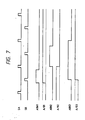
- Figure 7 is a timing chart showing signal waveforms in the various portions of the circuit shown in Figure 6.
- the reference numeral 1 designates an input terminal for inputting an error signal
- the reference numeral 2 denotes a sample hold (hereinafter referred to as S/H) circuit A to which the error signal is input
- the reference numeral 3 designates a sample hold (S/H) circuit B to which the same signal to that to the circuit 2 is input.
- the reference numeral 4 denotes an abnormality detecting circuit for the error signal to which the same signal as that to the circuits 2 and 3 is input.
- the abnormality detecting circuit 4 when during the operation of a control system, the error signal assumes a level outside a predetermined allowable range, the abnormality detecting circuit 4 outputs an abnormality detection signal ABN (hereinafter referred to as the ABN signal) indicative of this fact, for example, by a window comparator, not shown.
- ABN abnormality detection signal
- the reference numeral 5 designates a judging circuit to which the ABN signal is input.
- This judging circuit 5 outputs a signal for controlling the sampling and holding operation of the S/H circuit A (hereinafter referred to as the SHA signal) and a signal for controlling the sampling and holding operation of the S/H circuit B (hereinafter referred to as the SHB signal), and outputs a selection signal indicating the output of which of the S/H circuit A and the S/H circuit B should be selected (hereinafter referred to as the A/B signal).
- the reference numeral 6 denotes a selector for selecting the output of one of the S/H circuit A and the S/H circuit B by said A/B signal.
- the reference numeral 7 designates an output terminal for outputting the selected signal.
- the output terminal 7 is connected to drive means such as AT and AF actuators, not shown.
- the reference numeral 8 denotes an input terminal for inputting the aforementioned ABN signal
- the reference numeral 9 designates a periodic pulse train generating circuit generating periodic pulse trains SA and SB differing in phase from each other.
- the reference numeral 10 denotes an S/H enabling circuit to which the periodic pulse trains SA and SB are input and also the ABN signal is input. This S/H enabling circuit 10 outputs the SHA signal and the SHB signal.
- the reference numeral 11 designates a monitoring circuit A to which the ABN signal and the periodic pulse train SA are input and which detects when the abnormality of the error signal occurs or terminates, for the operative state of the S/H circuit A
- the reference numeral 12 denotes a monitoring circuit B to which the ABN signal and the periodic pulse train SB are input and which detects when the abnormality of the error signal occurs or terminates for the operative state of the S/H circuit B.
- the reference numeral 13 designates a select signal generating circuit generating an A/B signal indicating which of the S/H circuit A 2 and the S/H circuit B 3 should be selected by signals output from the monitoring circuit A 11 and the monitoring circuit B 12.
- FIG 7 is a timing chart schematically showing the operation of the present invention.
- SA and SB are the aforementioned periodic pulse trains differing in phase from each other, and when there is no abnormality in the error signal, the sampling operation of the sample hold circuits is executed in a time section corresponding to the "High” (hereinafter shown as "H") level of each periodic pulse train. Also, the holding operation is executed in a time section corresponding to the "Low” (hereinafter shown as "L”) level of each periodic pulse train.
- ABN1, ABN2 and ABN3 show the representative forms of the ABN signal output by the abnormality detecting circuit 4 of Figure 5 which has detected abnormality in the error signal, and they differ in the timing of generation and termination for the periodic pulse trains SA and SB from one another.
- A/B1, A/B2 and A/B3 are selection signals in the respective forms.
- the abnormality detecting circuit 4 when a state in which no abnormality of the AT and/or AF control is found continues, the magnitude of the error signal is within a predetermined allowable range and therefore, the abnormality detecting circuit 4 outputs a signal ABN of "L" level. Also, in the judging circuit 5, the signal ABN is at "L” level and therefore, the monitoring circuit A 11 and the monitoring curcuit B 12 do not effect the change-over of the S/H portion, and the signal A/B continues to keep “H” level or "L” level. Further, in the judging circuit 5, the periodic pulse trains SA and SB differing in phase from each other are output as sample hold signals SHA and SHB, respectively, without being limited by the S/H enabling circuit 10.
- the signal SHA is input, and the error signal is sampled during the period of "H” level and is held during the period of "L” level.
- the signal SHB is likewise input, and the error signal is sampled during the period of "H” level and is held during the period of "L” level.
- the selector 6 the S/H output of the side selected by the polarity of the signal A/B is output from the output terminal 7.
- the abnormality detection signal ABN1 is generated during the holding period of the S/H circuit A 2 and terminates during the same holding period.
- the monitoring circuit A 11 does not change over the S/H circuit because the signal ABN1 is generated and terminates during the holding period of the S/H circuit 2.
- the monitoring circuit B 12 remains inoperative although it detects the "H" level of the periodic pulse train SB during the generation of the signal ABN1.
- the monitoring circuit A 11 and the monitoring circuit B 12 chefsly monitor whether the abnormality detection signal ABN1 is generated and/or terminates when the periodic pulse trains SA and SB are in the "H" level state.
- the S/H enabling circuit 10 does not allow the passage of the periodic pulse train SB (the first pulse of Figure 7) generated from the periodic pulse train generating circuit 9 when the signal ABN is being generated and therefore, in the S/H circuit B 3, sampling is not effected during this time, but the holding of the value sampled before abnormality occurs in the error signal is continued.
- the monitoring circuit A 11 and the monitoring ciruit B 12 hold the value before the occurrence of abnormality irrespective of the occurrence and termination of the abnormality of the error signal.
- the S/H circuit selected before the abnormality remains selected.
- the signal ABN2 is such that abnormality occurs in the error signal when the periodic pulse train SA is at "H" level, i.e., when the S/H circuit A 2 is sampling, and terminates during the original holding period.
- the monitoring circuit A 11 detects that the abnormality detection signal ABN2 has been generated when the periodic pulse train SA is in the "H" level state. Then, it confirms that the S/H circuit B 3 which has already fallen the holding state has sampled a normal error signal, and outputs to the select signal generating circuit 13. A demand signal for driving an actuator, not shown, by the output of the S/H circuit B 3. In response to this, the select signal generating circuit 13 immediately renders the signal A/B 2 into "L" level.
- the S/H enabling circuit 10 does not allow the passage of the periodic pulse train SB (the second pulse of Figure 7) subsequently generated. That is, it discontinues the sampling operation of the S/H circuit B during the "H" level period of the signal ABN2. Also, the monitoring circuit B 11 remains inoperative during this time, and a demand signal for selecting the output of the S/H circuit a is not generated.
- abnormality occurs when the periodic pulse train SB is at "H” level, that is, when the S/H circuit B is sampling, and the abnormality of the error signal terminates when the periodic pulse train SA is at "H” level, that is, when the S/H circuit A is sampling.
- the monitoring circuit B 12 detects that the abnormality detection signal ABN3 has been generated when the periodic pulse train SB is in the "H" level state. Then, it confirms that the S/H circuit A 2 which has already fallen the holding state has sampled a normal error signal, and outputs to the select signal generating circuit 13 a demand signal for selecting the output of the S/H circuit A 2.
- the select signal generating circuit 13 immediately renders the signal A/B into "H” level. Further, the S/H enabling circuit 10 does not aloow the passage of the subsequent periodic pulse train SA (the second pulse of Figure 7) and periodic pulse train SB (the second and third pulses of Figure 7) and discontinues the sampling operation of the S/H circuit A and the S/H circuit B during the period when the abnormality detection signal ABN3 is at "H" level.
- the monitoring circuit A 11 detects that the signal ABN3 assumes "L" level, that is, the abnormality of the error signal has terminated (for example, due to its having passed the region of dust, flaw or the like), when the periodic pulse train SA (the third pulse of Figure 7) subsequently generated is in the "H" level state, but becomes inoperative because the S/H circuit B 3 is not performing the sampling operation at the timing of the periodic pulse train SB (the second pulse of Figure 7) immediately before.
- Figure 8 is a circuit diagram showing a specific example of the judging circuit shown in Figure 6.
- the reference numeral 21 designates a three-input AND circuit for gating the periodic pulse train SA by the inverted signal (hereinafter referred to as ABN ) of the signal ABN or the output of a D-type flip-flop 26 which will be described later.
- the AND circuit 21 outputs a signal SHA.
- the reference numeral 22 denotes a three-input AND circuit for gating the periodic pulse train SB by the signal ABN or the output of a D-type flip-flop 30 which will be described later.
- the AND circuit 22 outputs a signal SHB.
- the reference numeral 23 designates a pulse generating circuit to which the signal ABN is input and which generates a pulse at a timing corresponding to the occurrence of abnormality of the error signal (the rising of the signal) and the termination of the abnormality (the falling of the signal), and the reference numeral 24 denotes an inverter for converting the signal ABN into the opposite polarity.
- the reference numeral 25 designates a D-type flip-flop to the D terminal and clear terminal of which the periodic pulse train SA is input and to the clock terminal of which is input a pulse corresponding to the rising/falling pulse of the signal ABN output by the pulse generating circuit 23.
- This flip-flop 25 detects the generation and/or the termination of the signal ABN when the periodic pulse train SA is in the "H" level state, and outputs a demand signal for selecting the output of the S/H circuit B 3.
- the reference numeral 26 denotes a D-type flip-flop to the D terminal of which the periodic pulse train SB is input and to the clear terminal of which is input a signal SHB inverted by an inverter 27 and to the clock terminal of which the signal ABN is input.
- This flip-flop 26 temporarily memorizes therein that abnormality has occured in the error signal when the periodic pulse train SB is in the "H" level state.
- the reference numeral 28 designates a two-input AND circuit for gating said demand signal output by the D-type flip-flop 25 by information temporarily memorized by the D-type flip-flop 26.
- the D-type flip-flops 25 and 26, the inverter 27 and the two-input AND circuit 28 together constitute the monitoring circuit A 11.
- the reference numeral 29 denotes a D-type flip-flop to the D terminal and clear terminal of which the periodic pulse train SB is input and to the clock terminal of which is input a pulse corresponding to the rising/falling pulse of the signal ABN output by the pulse generating circuit 23.
- This flip-flop 29 detects the generation and/or termination of the signal ABN when the periodic pulse train SB is in the "H" level state, and outputs a demand signal for selecting the output of the S/H circuit A 2.
- the reference numeral 30 designates a D-type flip-flop to the D terminal of which the periodic pulse train SA is input and to the clock terminal of which the signal ABN is input and to the clear terminal of which is input a sample hold signal SHA inverted by an inverter 31.
- This flip-flop 30 temporarily memorizes therein that abnormality has occurred in the error signal when the periodic pulse train SA is in the "H" level state.
- the reference numeral 32 denotes a two-input AND circuit for gating said demand signal output by the D-type flip-flop 29 by information temporarily memorized by the D-type flip-flop 30.
- the D-type flip flops 29 and 30, the inverter 31 and the two-input AND circuit 32 together constitute the monitoring circuit B 12.
- the reference numeral 33 designates an RS-type flip-flop set by the output signal PA of the gate portion 28 and reset by the output signal PB of the gate portion 32. This flip-flop 33 outputs the selection signal A/B of the sample hold circuits.
- FIGS 9 to 11 are timing charts showing the timing at which the abnormality of the error signal occurs for the periodic pulse trains SA and SB and the timing until the selection signal A/B is generated, and only representative signals are shown in these figures.
- Figure 9 shows a case where the abnormality occurrence detection signal ABN is generated during the second holding period of the periodic pulse train SA (the "L" level period from after the second pulse of the periodic pulse train SA of Figure 9 is generated until the third pulse is generated) and the first holding period of the periodic pulse train SB, and terminates during the generation of the fourth pulse of the periodic pulse train SA (the "H" level period of the fourth pulse of Figure 9).
- the output of the inverter 24 is also at "H” level and the gates 21 and 22 constituting the S/H enabling circuit 10 become open, and the periodic pulse trains SA and SB are imparted as sample hold signals SHA and SHB, respectively, to the S/H circuit A 2 and the S/H circuit B 3.
- the same error signal is sampled when it is at "H” level at different phase timings, and the holding operation is performed at "L” level.
- the D-type flip-flops 25 and 29 have no clock input thereto and are cleared by periodic pulse trains SA and SB and therefore, the Q output assumes "L” level. Therefore, the outputs of the gates 28 and 32 are at "L” level. Accordingly, the state of the RS-type flip-flop 33 does not change, but continues to keep an output of "H" level or "L” level selected before.
- the periodic pulse trains SA and SB are being held at "L” level, and a pulse corresponding to the rising of the signal ABN is input as a clock to the rising/falling detecting D-type flip-flops 25 and 29 with the input to the D terminals thereof being in the "L” level state and therefore, in this case, no transition of the state takes place and the Q output continuedly outputs "L” level.
- the periodic pulse trains SA and SB are not allowed to pass therethrough during the period until the signal ABN inverted by the inverter 24 transits to "L” level and the abnormal state of the error signal is released.
- the second pulse of the sample hold signal SHA of Figure 9 and the second and third pulses (the pulses depicted by broken lines) of the sample hold signal SHB are erased.
- both of the S/H circuit A 2 and the S/H circuit B 3 continue their holding state.
- neither of the D-type flip-flops 26 and 30 does not effect state transition.
- the RS-type flip-flop 33 effects state transition because the signals PA and PB are not generated in this section.
- the periodic pulse train SB is being held at "L” level and as previously described, the state of the rising/falling detecting D-type flip-flop 29 does not transit.
- the periodic pulse train SA is in the "H” level state, and the input to the D terminal of the D-type flip-flop 25 becomes “H” and at this timing, a pulse corresponding to the falling of the signal ABN is output from the pulse generating circuit 23 and input to the clock terminal.
- the Q output of the D-type flip-flop 25 assumes "H” level (because the periodic pulse train SA is input to the clear terminal) and the pulse output continues until the periodic pulse train SA assumes "L” level.
- Figure 10 shows a case where the abnormality of the error signal occurs during the generation of the second pulse of the periodic pulse train SA (i.e., during the sampling by the S/H circuit A 2) and terminates during the generation of the fourth pulse.
- the periodic pulse train SB is at "L” level and the S/H circuit B 3 is in its holding state, and as described in connection with Figure 9, the input to the D terminal of the D-type flip-flop 29 is “L” and therefore this flip-flop continuedly puts out “L” output and the transition of the state thereof does not take place.
- the input to the D terminal of the D-type flip-flop 25 is "H” and a clock corresponding to the rising of the signal ABN is input to this flip-flop and therefore, the same pulse as the signal PA shown in Figure 10 is generated.
- the output pulse is generated in the time section from after the signal ABN has risen until the flip-flop 25 is cleared by the "L" level portion of the periodic pulse SA.
- the input to the D terminal of the D-type flip-flop 26 is “L” and therefore, this flip-flop continuedly puts out “H” output and the transition of the state thereof does not take place.
- the input to the D terminal of the D-type flip-flop 30 is at "H” level and the rising clock of the signal ABN is input to this flip-flop, and the Q output PBE thereof transits to "L” level. Accordingly, the gate 28 becomes open and outputs a pulse signal PA, and the gate 29 becomes closed. Therefore, the RS-type flip-flop assumes "L” level independently of "H” level or “L” level output hitherto, and selects the output of the S/H circuit B 3.
- the gates 21 and 22 are rendered closed and therefore, the sample hold signals SHA and SHB of Figure 10 have their pulse regions which are indicated by broken lines erased.
- the periodic pulse train SB is in the holding state ("L" level) and the states of the D-type flip-flops 26 and 29 do not transit.
- the D-type flip-flop 30 has no rising clock input thereto, but the sample hold signal SHA, though imperfect in its pulse width, is put out as the output of the gate 21, and clears the flip-flop 30 through the inverter 31. Therefore, the Q output PBE transits to "H".
- the input to the D terminal of the D-type flip-flop 25 is "H” and a pulse corresponding to the falling pulse of the signal ABN is input as a clock thereto and therefore, there is generated the second pulse of the signal PA shown in Figure 10 (the output pulse disappears in the "L” level section of the periodic pulse SA). Accordingly, the gate 32 is closed because the Q output of the D-type flip-flop 29 continuedly puts out “L” level, and the gate 28 is open and outputs a pulse PA because the signal PAE is "H". However, since the RS-type flip-flop is already set to "L” output, the transition of the state thereof does not take place.
- Figure 11 shows a case where the abnormality of the error signal occurs during the generation of the first pulse of the periodic pulse train SB (i.e., during the sampling operation of the S/H circuit B 3) and terminates during the generation of the third pulse of the periodic pulse train SA.
- the periodic pulse train SA is at "L” level and the S/H circuit A 2 is in its holding state, and the inputs to the D terminals of the D-type flip-flops 25 and 30 are "L” and therefore, the transition of the states of these flip-flops does not take place. That is, the output of the D-type flip-flop 25 maintains “L” level and the Q output PBE of the D-type flip-flop 30 maintains "H" level.
- the inputs to the D terminals of the D-type flip-flops 26 and 29 are at "H” level, and the Q output PAE of the D-type flip-flop 26 transits to "L” level, and the D-type flip-flop 29 generates a pulse, not shown, at the same timing as the pulse shown in the signal PB of Figure 10, from the rising of the signal ABN until the flip-flop 29 is cleared by the "L" level of the periodic pulse train SB. Accordingly, the signal PAE assumes “L” level and the input end of the gate 28 becomes closed, and the output signal PA remains at "L” level.
- the input end of the gate 32 is open and puts out the output pulse of the D-type flip-flop 29 as an output signal PB.
- the RS-type flip-flop 33 renders the selection signal A/B as the output signal into "H” level irrespective of its state hitherto.
- the gates 21 and 22 are rendered closed during the period for which the abnormality detection signal ABN is "H", and the "H" level of the sample hold signals SHA and SHB is deleted and the S/H circuit A 2 and the S/H circuit B 3 are brought into their holding state.
- the signal PA indicated by broken line in Figure 11 is pulse-output
- the gate 21 is closed and the third/pulse of the sample hold signal SHA is completely deleted. That is, since the abnormality of the sampling by the selected sample hold circuit (in this case, the S/H circuit B 3) is temporarily memorized during the change-over of the selection signal, operation is performed so that selection of a wrong sample hold circuit (indicated by broken line in Figure 11 A/B) may not be executed. At the same time, operation is performed so as not to cause the abnormality of the sampling by the sample hold circuit being selected (in this case, the S/H circuit A 2).
- the D-type flip-flop 26 is cleared by the inverted output SHB of the sample hold signal SHB output from the gate 22 which has become open after the abnormality has been released, restores its Q output PAE to "H" level, restores the gate 21 to its open state, and returns to its normal operation.
- Figures 9 to 11 are shown as typical examples because a similar operation is performed even if the timing of the generation of the abnormality detection signal ABN relative to the periodic pulse trains SA and SB becomes opposite between the A system and the B system.
- the S/H enabling circuit instead of being constructed of gate logic, may be constructed so as to stop the generation of the periodic pulse trains.
- the times of generation and termination of the abnormality detection signal ABN of the error signal may be synchronized with the timing of the periodic pulse trains or the like so that the sampling operation by an incomplete sampling pulse may not be started.
- SA, SB and ABN represent the same signals as the signals already described
- ABN1 represents the Q output of a D-type flip-flop to the D terminal of which the signal ABN is input and to the clock terminal of which the logic sum of the periodic pulse trains SA and SB are input
- ABN2 represents the logic sum of the signal ABN and the signal ABN1
- the rear edge is synchronized with the fore edge of the periodic pulse train SA or SB.
- design may be made such that the signal ABN2 is made to fall before the start of the sampling by the timing pulses forming the same periodic pulse train.
Landscapes
- Optical Recording Or Reproduction (AREA)
- Moving Of The Head To Find And Align With The Track (AREA)
Applications Claiming Priority (2)
| Application Number | Priority Date | Filing Date | Title |
|---|---|---|---|
| JP1150059A JP2683104B2 (ja) | 1989-06-12 | 1989-06-12 | 情報記録再生装置 |
| JP150059/89 | 1989-06-12 |
Publications (3)
| Publication Number | Publication Date |
|---|---|
| EP0403196A2 true EP0403196A2 (fr) | 1990-12-19 |
| EP0403196A3 EP0403196A3 (fr) | 1991-11-13 |
| EP0403196B1 EP0403196B1 (fr) | 1995-08-23 |
Family
ID=15488613
Family Applications (1)
| Application Number | Title | Priority Date | Filing Date |
|---|---|---|---|
| EP90306321A Expired - Lifetime EP0403196B1 (fr) | 1989-06-12 | 1990-06-11 | Appareil d'enregistrement/de la reproduction optique avec une pluralité de circuits d'échantillonment |
Country Status (4)
| Country | Link |
|---|---|
| US (1) | US5235580A (fr) |
| EP (1) | EP0403196B1 (fr) |
| JP (1) | JP2683104B2 (fr) |
| DE (1) | DE69021784T2 (fr) |
Cited By (2)
| Publication number | Priority date | Publication date | Assignee | Title |
|---|---|---|---|---|
| WO1992014242A1 (fr) * | 1991-02-09 | 1992-08-20 | Deutsche Thomson-Brandt Gmbh | Appareil optique d'enregistrement et/ou de reproduction |
| US5835121A (en) * | 1995-04-21 | 1998-11-10 | Xerox Corporation | Pixel exposure control for a raster output scanner in an electrophotographic printer |
Families Citing this family (6)
| Publication number | Priority date | Publication date | Assignee | Title |
|---|---|---|---|---|
| US5283775A (en) * | 1992-12-14 | 1994-02-01 | International Business Machines, Inc. | Split detector system for direct read-while-write operation on magneto-optic media |
| JP2001229617A (ja) | 2000-02-16 | 2001-08-24 | Mitsubishi Electric Corp | 光ディスク用信号検出回路 |
| KR20020008657A (ko) * | 2000-07-25 | 2002-01-31 | 이계안 | 연료탱크내의 연료유동 및 비산방지장치 |
| US7475135B2 (en) * | 2005-03-31 | 2009-01-06 | International Business Machines Corporation | Systems and methods for event detection |
| US9372485B2 (en) | 2011-11-02 | 2016-06-21 | Smc Kabushiki Kaisha | Flow rate control device |
| CN116915254A (zh) * | 2023-09-14 | 2023-10-20 | 鹏元晟高科技股份有限公司 | 多路电压隔离采样电路 |
Citations (3)
| Publication number | Priority date | Publication date | Assignee | Title |
|---|---|---|---|---|
| EP0227445A2 (fr) * | 1985-12-21 | 1987-07-01 | Sony Corporation | Procédés et appareil de servocommande de focalisation |
| EP0306179A2 (fr) * | 1987-08-31 | 1989-03-08 | Canon Kabushiki Kaisha | Appareil d'enregistrement et de reproduction des informations avec moyens de détection des fautes de suivi de piste |
| US4821251A (en) * | 1983-11-18 | 1989-04-11 | Canon Kabushiki Kaisha | Method and apparatus for recording or reproducing information in or from only a sector of an optical disk track without any defect by shifting a light beam to an adjacent track before a defective sector |
Family Cites Families (7)
| Publication number | Priority date | Publication date | Assignee | Title |
|---|---|---|---|---|
| KR870006556A (ko) * | 1985-12-13 | 1987-07-13 | 미쓰다 가쓰시게 | 트랙킹서보 제어장치 |
| JP2796285B2 (ja) * | 1986-07-11 | 1998-09-10 | 株式会社日立製作所 | トラッキング方法及びそれを用いた光ディスク装置 |
| JP2523555B2 (ja) * | 1986-12-19 | 1996-08-14 | 株式会社日立製作所 | 光スポットの制御方法及び位置制御装置 |
| US4860271A (en) * | 1987-03-13 | 1989-08-22 | Pioneer Electronic Corporation | Servo circuit for generating a tracking error signal for optical disk player |
| US4982392A (en) * | 1987-07-10 | 1991-01-01 | Ricoh Company, Ltd. | Stabilized optical pick-up device inhibiting the effect of the focus error signal at the start and end of a data region |
| JPS6437729A (en) * | 1987-08-04 | 1989-02-08 | Canon Kk | Optical information recording and reproducing device |
| JP2585036B2 (ja) * | 1987-12-25 | 1997-02-26 | 京セラ株式会社 | 光学式情報記録再生装置のトラッキングデフェクト解消方法 |
-
1989
- 1989-06-12 JP JP1150059A patent/JP2683104B2/ja not_active Expired - Fee Related
-
1990
- 1990-06-11 US US07/536,024 patent/US5235580A/en not_active Expired - Fee Related
- 1990-06-11 DE DE69021784T patent/DE69021784T2/de not_active Expired - Fee Related
- 1990-06-11 EP EP90306321A patent/EP0403196B1/fr not_active Expired - Lifetime
Patent Citations (3)
| Publication number | Priority date | Publication date | Assignee | Title |
|---|---|---|---|---|
| US4821251A (en) * | 1983-11-18 | 1989-04-11 | Canon Kabushiki Kaisha | Method and apparatus for recording or reproducing information in or from only a sector of an optical disk track without any defect by shifting a light beam to an adjacent track before a defective sector |
| EP0227445A2 (fr) * | 1985-12-21 | 1987-07-01 | Sony Corporation | Procédés et appareil de servocommande de focalisation |
| EP0306179A2 (fr) * | 1987-08-31 | 1989-03-08 | Canon Kabushiki Kaisha | Appareil d'enregistrement et de reproduction des informations avec moyens de détection des fautes de suivi de piste |
Cited By (3)
| Publication number | Priority date | Publication date | Assignee | Title |
|---|---|---|---|---|
| WO1992014242A1 (fr) * | 1991-02-09 | 1992-08-20 | Deutsche Thomson-Brandt Gmbh | Appareil optique d'enregistrement et/ou de reproduction |
| US5867461A (en) * | 1991-02-09 | 1999-02-02 | Deutsche Thomson-Brandt Gmbh | Optical recording and reproducing apparatus with servo compensation for detected defects and external shocks |
| US5835121A (en) * | 1995-04-21 | 1998-11-10 | Xerox Corporation | Pixel exposure control for a raster output scanner in an electrophotographic printer |
Also Published As
| Publication number | Publication date |
|---|---|
| EP0403196A3 (fr) | 1991-11-13 |
| JP2683104B2 (ja) | 1997-11-26 |
| EP0403196B1 (fr) | 1995-08-23 |
| DE69021784D1 (de) | 1995-09-28 |
| JPH0316029A (ja) | 1991-01-24 |
| DE69021784T2 (de) | 1996-02-08 |
| US5235580A (en) | 1993-08-10 |
Similar Documents
| Publication | Publication Date | Title |
|---|---|---|
| KR920006307B1 (ko) | 광 픽업(Pick up)의 트랙점프(track jump)장치. | |
| EP0767456B1 (fr) | Méthode et appareil de commande d'asservissement de focalisation | |
| CA1314983C (fr) | Appareil optique de traitement d'information pouvant maintenir un dispositif optique dans une situation predeterminee en cas de defaillance de la commande de centrage ou de focalisation | |
| EP0403196B1 (fr) | Appareil d'enregistrement/de la reproduction optique avec une pluralité de circuits d'échantillonment | |
| EP0505252A2 (fr) | Méthode et circuit pour la correction du signal de passage par zéro dans un système de disque optique | |
| EP0683487B1 (fr) | Appareil d'enregistrement/lecture optique d'informations ayant comme une fonction d'empêcher la surécriture | |
| EP0424980A2 (fr) | Appareil de disques optiques et appareil d'emmagasinage d'information | |
| JPH0363135B2 (fr) | ||
| GB2174530A (en) | Optical record medium (card) recording/reproduction | |
| JPS5994249A (ja) | トラツキング・エラ−検出信号発生回路 | |
| KR100235996B1 (ko) | 트랙 점프 장치 | |
| US5313440A (en) | Track crossing method using dual counters | |
| JP2589072B2 (ja) | デイスク再生装置 | |
| US6222798B1 (en) | Track jump for optical information recording and reproducing method and device | |
| US6711104B2 (en) | Disk reading apparatus | |
| JPH02134732A (ja) | 情報記録再生装置 | |
| EP0393885A2 (fr) | Appareil d'enregistrement et de reproduction optique | |
| KR100257621B1 (ko) | 광디스크시스템의 트랙점프장치 및 그 제어방법 | |
| JPH0520692A (ja) | 情報記録再生装置 | |
| KR100230236B1 (ko) | 광 디스크의 포커싱 서보 장치 | |
| JPH06309678A (ja) | アクセス制御装置 | |
| KR19990035343A (ko) | 광디스크 시스템의 트랙점프제어방법 | |
| JPS5823331A (ja) | 光学ヘツドの制御装置 | |
| JPH0439130B2 (fr) | ||
| JPH02214025A (ja) | 光学的情報記録再生装置 |
Legal Events
| Date | Code | Title | Description |
|---|---|---|---|
| PUAI | Public reference made under article 153(3) epc to a published international application that has entered the european phase |
Free format text: ORIGINAL CODE: 0009012 |
|
| AK | Designated contracting states |
Kind code of ref document: A2 Designated state(s): DE FR GB NL |
|
| 17P | Request for examination filed |
Effective date: 19901231 |
|
| PUAL | Search report despatched |
Free format text: ORIGINAL CODE: 0009013 |
|
| AK | Designated contracting states |
Kind code of ref document: A3 Designated state(s): DE FR GB NL |
|
| 17Q | First examination report despatched |
Effective date: 19940209 |
|
| GRAA | (expected) grant |
Free format text: ORIGINAL CODE: 0009210 |
|
| AK | Designated contracting states |
Kind code of ref document: B1 Designated state(s): DE FR GB NL |
|
| REF | Corresponds to: |
Ref document number: 69021784 Country of ref document: DE Date of ref document: 19950928 |
|
| ET | Fr: translation filed | ||
| PLBE | No opposition filed within time limit |
Free format text: ORIGINAL CODE: 0009261 |
|
| STAA | Information on the status of an ep patent application or granted ep patent |
Free format text: STATUS: NO OPPOSITION FILED WITHIN TIME LIMIT |
|
| 26N | No opposition filed | ||
| REG | Reference to a national code |
Ref country code: GB Ref legal event code: IF02 |
|
| PGFP | Annual fee paid to national office [announced via postgrant information from national office to epo] |
Ref country code: GB Payment date: 20030528 Year of fee payment: 14 |
|
| PGFP | Annual fee paid to national office [announced via postgrant information from national office to epo] |
Ref country code: FR Payment date: 20030620 Year of fee payment: 14 |
|
| PGFP | Annual fee paid to national office [announced via postgrant information from national office to epo] |
Ref country code: DE Payment date: 20030626 Year of fee payment: 14 |
|
| PGFP | Annual fee paid to national office [announced via postgrant information from national office to epo] |
Ref country code: NL Payment date: 20030630 Year of fee payment: 14 |
|
| PG25 | Lapsed in a contracting state [announced via postgrant information from national office to epo] |
Ref country code: GB Free format text: LAPSE BECAUSE OF NON-PAYMENT OF DUE FEES Effective date: 20040611 |
|
| PG25 | Lapsed in a contracting state [announced via postgrant information from national office to epo] |
Ref country code: NL Free format text: LAPSE BECAUSE OF NON-PAYMENT OF DUE FEES Effective date: 20050101 Ref country code: DE Free format text: LAPSE BECAUSE OF NON-PAYMENT OF DUE FEES Effective date: 20050101 |
|
| GBPC | Gb: european patent ceased through non-payment of renewal fee |
Effective date: 20040611 |
|
| PG25 | Lapsed in a contracting state [announced via postgrant information from national office to epo] |
Ref country code: FR Free format text: LAPSE BECAUSE OF NON-PAYMENT OF DUE FEES Effective date: 20050228 |
|
| NLV4 | Nl: lapsed or anulled due to non-payment of the annual fee |
Effective date: 20050101 |
|
| REG | Reference to a national code |
Ref country code: FR Ref legal event code: ST |