EP0400670A2 - Halbleiterspeicheranordnung und Verfahren zu ihrer Herstellung - Google Patents
Halbleiterspeicheranordnung und Verfahren zu ihrer Herstellung Download PDFInfo
- Publication number
- EP0400670A2 EP0400670A2 EP90110472A EP90110472A EP0400670A2 EP 0400670 A2 EP0400670 A2 EP 0400670A2 EP 90110472 A EP90110472 A EP 90110472A EP 90110472 A EP90110472 A EP 90110472A EP 0400670 A2 EP0400670 A2 EP 0400670A2
- Authority
- EP
- European Patent Office
- Prior art keywords
- impurity
- region
- floating gate
- forming
- conductivity type
- Prior art date
- Legal status (The legal status is an assumption and is not a legal conclusion. Google has not performed a legal analysis and makes no representation as to the accuracy of the status listed.)
- Granted
Links
- 239000004065 semiconductor Substances 0.000 title claims abstract description 78
- 238000004519 manufacturing process Methods 0.000 title claims abstract description 17
- 239000012535 impurity Substances 0.000 claims abstract description 128
- 239000000758 substrate Substances 0.000 claims description 42
- 238000000034 method Methods 0.000 claims description 14
- 238000002513 implantation Methods 0.000 claims description 13
- 238000005468 ion implantation Methods 0.000 claims description 13
- 238000002955 isolation Methods 0.000 claims description 10
- 230000003647 oxidation Effects 0.000 claims description 10
- 238000007254 oxidation reaction Methods 0.000 claims description 10
- 238000009413 insulation Methods 0.000 claims description 7
- 150000002500 ions Chemical class 0.000 claims description 4
- 238000009792 diffusion process Methods 0.000 claims 2
- 239000006185 dispersion Substances 0.000 claims 2
- -1 boron ions Chemical class 0.000 description 15
- 229910052785 arsenic Inorganic materials 0.000 description 11
- 229910052796 boron Inorganic materials 0.000 description 10
- 229910021420 polycrystalline silicon Inorganic materials 0.000 description 7
- 229920005591 polysilicon Polymers 0.000 description 7
- 229920002120 photoresistant polymer Polymers 0.000 description 6
- ZOXJGFHDIHLPTG-UHFFFAOYSA-N Boron Chemical compound [B] ZOXJGFHDIHLPTG-UHFFFAOYSA-N 0.000 description 3
- RQNWIZPPADIBDY-UHFFFAOYSA-N arsenic atom Chemical compound [As] RQNWIZPPADIBDY-UHFFFAOYSA-N 0.000 description 3
- QVGXLLKOCUKJST-UHFFFAOYSA-N atomic oxygen Chemical compound [O] QVGXLLKOCUKJST-UHFFFAOYSA-N 0.000 description 3
- 238000010586 diagram Methods 0.000 description 3
- 230000005684 electric field Effects 0.000 description 3
- 229910052760 oxygen Inorganic materials 0.000 description 3
- 239000001301 oxygen Substances 0.000 description 3
- 238000004528 spin coating Methods 0.000 description 3
- 238000000137 annealing Methods 0.000 description 2
- 230000015572 biosynthetic process Effects 0.000 description 2
- VYPSYNLAJGMNEJ-UHFFFAOYSA-N Silicium dioxide Chemical compound O=[Si]=O VYPSYNLAJGMNEJ-UHFFFAOYSA-N 0.000 description 1
- 230000001133 acceleration Effects 0.000 description 1
- 238000005229 chemical vapour deposition Methods 0.000 description 1
- 238000000151 deposition Methods 0.000 description 1
- 238000010438 heat treatment Methods 0.000 description 1
- 239000011261 inert gas Substances 0.000 description 1
- 238000000059 patterning Methods 0.000 description 1
- 229910052814 silicon oxide Inorganic materials 0.000 description 1
Images




Classifications
-
- H—ELECTRICITY
- H10—SEMICONDUCTOR DEVICES; ELECTRIC SOLID-STATE DEVICES NOT OTHERWISE PROVIDED FOR
- H10D—INORGANIC ELECTRIC SEMICONDUCTOR DEVICES
- H10D30/00—Field-effect transistors [FET]
- H10D30/60—Insulated-gate field-effect transistors [IGFET]
- H10D30/68—Floating-gate IGFETs
- H10D30/681—Floating-gate IGFETs having only two programming levels
- H10D30/684—Floating-gate IGFETs having only two programming levels programmed by hot carrier injection
- H10D30/685—Floating-gate IGFETs having only two programming levels programmed by hot carrier injection from the channel
-
- H—ELECTRICITY
- H10—SEMICONDUCTOR DEVICES; ELECTRIC SOLID-STATE DEVICES NOT OTHERWISE PROVIDED FOR
- H10D—INORGANIC ELECTRIC SEMICONDUCTOR DEVICES
- H10D30/00—Field-effect transistors [FET]
- H10D30/01—Manufacture or treatment
- H10D30/021—Manufacture or treatment of FETs having insulated gates [IGFET]
- H10D30/0411—Manufacture or treatment of FETs having insulated gates [IGFET] of FETs having floating gates
-
- H—ELECTRICITY
- H10—SEMICONDUCTOR DEVICES; ELECTRIC SOLID-STATE DEVICES NOT OTHERWISE PROVIDED FOR
- H10D—INORGANIC ELECTRIC SEMICONDUCTOR DEVICES
- H10D30/00—Field-effect transistors [FET]
- H10D30/60—Insulated-gate field-effect transistors [IGFET]
- H10D30/68—Floating-gate IGFETs
- H10D30/6891—Floating-gate IGFETs characterised by the shapes, relative sizes or dispositions of the floating gate electrode
-
- H—ELECTRICITY
- H10—SEMICONDUCTOR DEVICES; ELECTRIC SOLID-STATE DEVICES NOT OTHERWISE PROVIDED FOR
- H10D—INORGANIC ELECTRIC SEMICONDUCTOR DEVICES
- H10D62/00—Semiconductor bodies, or regions thereof, of devices having potential barriers
- H10D62/10—Shapes, relative sizes or dispositions of the regions of the semiconductor bodies; Shapes of the semiconductor bodies
- H10D62/17—Semiconductor regions connected to electrodes not carrying current to be rectified, amplified or switched, e.g. channel regions
- H10D62/213—Channel regions of field-effect devices
- H10D62/221—Channel regions of field-effect devices of FETs
- H10D62/235—Channel regions of field-effect devices of FETs of IGFETs
- H10D62/299—Channel regions of field-effect devices of FETs of IGFETs having lateral doping variations
- H10D62/307—Channel regions of field-effect devices of FETs of IGFETs having lateral doping variations the doping variations being parallel to the channel lengths
-
- H—ELECTRICITY
- H10—SEMICONDUCTOR DEVICES; ELECTRIC SOLID-STATE DEVICES NOT OTHERWISE PROVIDED FOR
- H10D—INORGANIC ELECTRIC SEMICONDUCTOR DEVICES
- H10D62/00—Semiconductor bodies, or regions thereof, of devices having potential barriers
- H10D62/60—Impurity distributions or concentrations
-
- H—ELECTRICITY
- H10—SEMICONDUCTOR DEVICES; ELECTRIC SOLID-STATE DEVICES NOT OTHERWISE PROVIDED FOR
- H10B—ELECTRONIC MEMORY DEVICES
- H10B69/00—Erasable-and-programmable ROM [EPROM] devices not provided for in groups H10B41/00 - H10B63/00, e.g. ultraviolet erasable-and-programmable ROM [UVEPROM] devices
Definitions
- This invention relates to a semiconductor memory device and a method of manufacturing the same.
- it relates to a semiconductor memory device provided with a control gate on top of a floating gate or a channel that is on a drain side, and a method of manufacturing such a semiconductor memory device.
- a conventional flash EEPROM type of semiconductor device has an n-type source and an n-type drain formed in the surface of a p-type semiconductor substrate, and a floating gate is formed in the proximity of the drain on top of an oxide film on a channel between the drain and source.
- a floating gate and a control gate are formed above an offset portion (F) between the floating gate end and the source end, with an oxide film thereunder.
- a p-type impurity region of an impurity concentration greater than that of the substrate is formed uniformly in the channel between the drain and source.
- this conventional semiconductor memory device has the following problem.
- the electric field can easily focus in this region, the generation probability of electrons injected into the floating gate is increased, and the memory cell write characteristics are improved.
- the threshold voltage V th of the offset transistor (hereinafter the transistor in the offset portion (F) will be called the offset transistor) also increases, making it difficult for current to flow in the memory cell and hence increasing access times. Conversely, if the concentration of the impurity in the impurity region is reduced, the threshold voltage V th of the offset transistor will drop, improving the memory cell's access times but making the memory cell write characteristics worse. Because of these conflicting problems, it is difficult to satisfy demands for both improved memory cell write characteristics and better access times in the conventional semiconductor memory device.
- an object of the present invention is to provide a semiconductor memory device that has good memory cell write characteristics and offset transistors with desired threshold voltages.
- Another object of the present invention is to provide a manufacturing method that can stably manufacture such a semiconductor memory device.
- a semiconductor memory device comprising: a semiconductor substrate of a first conductivity type; a source and a drain of a second conductivity type, the source and the drain being provided separately in the surface of the semiconductor substrate; a channel between the source and the drain; a first impurity region of the first conductivity type, the first impurity region having an impurity concentration greater than that of the semiconductor substrate, and being provided in the drain side of the channel; a second impurity region of the first conductivity type, the second impurity region having an impurity concentration greater than that of the semiconductor substrate but less than that of the first impurity region, and being provided in the source side of the channel; a floating gate provided on top of the first impurity region, with an isolation film thereunder; and a control gate provided on top of the floating gate and the first impurity region, with an isolation film thereunder.
- the threshold voltage of the offset transistor can be set to any desired value.
- the second impurity region with a concentration of an impurity of the first conductivity type that is greater than that of the first impurity region is provided in the channel under the floating gate, the number of electrons implanted into the floating gate can be increased, improving the memory cell's write characteristics.
- a method of manufacturing a semiconductor memory device comprising the steps of forming a first impurity region in a specific region of the surface of a semiconductor substrate of a first conductivity type, the first impurity region having an impurity concentration greater than that of the semiconductor substrate; forming a floating gate corresponding to a high-impurity-concentration region above an isolation film formed over the semiconductor substrate of the first conductivity type; forming a second impurity region of the first conductivity type adjacent to the first impurity region, the second impurity region having an impurity concentration greater than that of the semiconductor substrate but less than that of the first impurity region, and being formed by ion implantation using as a mask the floating gate and a layer of resist patterned so as to define a channel width; forming a drain region in the first impurity region, on the side thereof opposite to the second impurity region, the drain region being a high-impurity-concentration region of a second conductivity type opposite to the first conductivity
- the above method is capable of providing in a simple manner the semiconductor memory device of the present invention.
- Figure 1 is a plan view of an example of a memory cell of a flash EEPROM (batch-erasable non-volatile memory) of a first embodiment of the present invention
- Figs. 2 and 3 are cross sectional views of the memory cell taken respectively along the lines A-A′ and B-B′ of Fig. 1.
- an n-type drain 6 and an n-type source 14 are formed separately on the surface of a p-type semiconductor substrate 1 on which an oxide film (SiO2) 2 has been formed as an insulation film.
- a floating gate 4 of polysilicon is formed on top of the oxide film 2 on a channel between the drain 6 and the source 14, in such a manner that it is disposed above the drain 6.
- a control gate 7 of polysilicon is formed over the floating gate 4 with an oxide film of (of SiO2) 63 therebetween and a channel between the floating gate 4 and the source 14 with the oxide film of (of SiO2) 2 therebetween.
- An oxide film (of SiO2) 64 is then formed over the control gate 7.
- a first impurity region 31 of an impurity concentration much greater than that of the semiconductor substrate 1 is provided below the floating gate 4, in contact with the drain 6, and a second impurity region 33 of an impurity concentration greater than that of the semiconductor substrate 1 but less than that of the first impurity region 31 is formed in the channel.
- the impurity concentration of the semiconductor substrate 1 is approximately 2 ⁇ 1015 cm ⁇ 3, that of the drain 6 is 1020 cm ⁇ 3 (at a position close to the surface), that of the source 14 is 1020 cm ⁇ 3 (at a position close to the surface), that of the first impurity region 31 is 1 ⁇ 1017 cm ⁇ 3 (at a position close to the surface), and that of the second impurity region 33 is 4 ⁇ 1016 cm ⁇ 3 (at a position close to the surface).
- an erase gate 20 that erases electrons implanted into the floating gate 4 is formed on this memory structure.
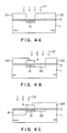
- a layer of resist is deposited on the oxide film 2 over the semiconductor substrate 1, using a spin coating method, and it is exposed to exposure light to form a patterned resist film 101.
- the resist film 101 is then used as a mask boron ions 111 are implanted into the semiconductor substrate 1 to form the first impurity region 31.
- the floating gate 4 made of polysilicon is selectively formed over the first impurity region 31, as shown in Fig. 4B.
- a resist film 102 is then deposited by spin coating and is patterned by exposure to light.
- the floating gate 4 and the resist film 102 are used as a mask for the implantation of boron ions 112 into the semiconductor substrate 1 to form the second impurity region 33 adjacent to the first impurity region 31.
- the dose at which the boron ions are implanted is less than that used during the implantation of the first impurity region 31, so the first impurity region 31 has a higher concentration of the boron impurity than the second impurity region 33.
- a resist film 103 is deposited by spin coating and is patterned by exposure to light, and the floating gate 4 and the resist film 103 are used as a mask for the implantation of arsenic ions 113 to form the drain 6, as shown in Fig. 4C.
- the arsenic ions are implanted at a dose of 5 ⁇ 1015 cm ⁇ 2 with an accelerating energy of 50 keV.
- the oxide film 63 having a thickness of e.g. 500 ⁇ is formed above the floating gate 4, using a method such as thermal oxidation, for example oxidation in an atmosphere of dry oxygen at approx. 1000°C, as shown in Fig. 4D.
- the control gate 7 is then formed over the floating gate 4 and the first impurity region 31, with the oxide films 63 and 2 thereunder.
- Arsenic ions 114 are implanted into the entire surface at a dose of 5 ⁇ 1015 cm ⁇ 2 with energy of 50 keV, using the control gate 7 as a mask, to form the source 14.
- the oxide film 64 is formed over the control gate 7 by a method such as thermal oxidation, to obtain the semiconductor memory device of the embodiment of the present invention shown in Fig. 2.
- the first impurity region 31 with its high concentration of p-type impurity is adjacent to the n-type drain 6, the electric field can easily focus. Since this increases the generation probability of electrons injected into the floating gate 4, the memory cell write characteristics are improved.
- the second impurity region 33 with its required impurity concentration that is lower than that of the first impurity region 31 is provided in the channel below the control gate 7, the threshold voltage V th of the memory cell's transistor can be set to any desired value. Therefore, current flows easily in the memory cell, and thus access times can be increased.
- the drain 6 and source 14 are formed separately on the surface of the p-type semiconductor substrate 1 on which the oxide film 2 that acts as an insulation film has been formed, and the first impurity region 31 is formed so as to surround the drain 6, of a p-type impurity of a higher concentration than that of the semiconductor substrate 1.
- the p-type second impurity region 33 is formed with an impurity concentration that is higher than that of the semiconductor substrate 1, but lower than that of the first impurity region 31, between the first impurity region 31 and the source 14.
- the floating gate 4 is formed above the channel, in such a way that it is in contact with the drain 6, with the oxide film 2 therebetween.
- the control gate 7 is formed above the floating gate 4 (with the oxide film 63 therebetween) and an offset portion (F) (with the oxide film 2 therebetween), then the oxide film 64 is formed over the surface of the floating gate 4.
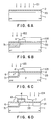
- boron ions 121 are implanted by an ion implantation method at a dose of 4 ⁇ 1012 cm ⁇ 2 with energy of 60 keV into the surface of the p-type semiconductor substrate 1 on which the oxide film 2 has been formed, to form the second impurity region 33 that has a higher impurity concentration than that of the semiconductor substrate 1.
- the floating gate 4 is formed at a desired position on the semiconductor substrate 1 by depositing a polysilicon film thereon by a CVD method then patterning it. A layer of resist is deposited and patterned to form a resist film 105.
- the resist film 105 and the floating gate 4 are used as a mask for the implantation of boron ions 122 to form the first impurity region 31.
- the boron ions 122 are implanted at a dose of 2 ⁇ 1013 cm ⁇ 2 with an accelerating voltage of 100 keV that is higher than that used during the ion implantation that formed the second impurity region 33, and, after the ion implantation, a thermal process (annealing at approx. 1000°C in inert gas (N2) atmosphere for 20 minutes) is employed to diffuse the first impurity region 31 into the semiconductor substrate 1.
- the resist film 105 and the floating gate 4 are again used as a mask for the implantation of arsenic ions 123 at a dose of 5 ⁇ 1015 cm ⁇ 2 using an acceleration energy of 50 keV to form the drain 6 in a self-aligning manner, as shown in Fig. 6C.
- the oxide (SiO2) film 63 having a thickness of 500 ⁇ is formed above the floating gate 4 by a thermal oxidation method, and the control gate 7 is formed above the floating gate 4 (with the oxide film 63 therebetween) and an offset portion (F) (with the oxide film 2 therebetween).
- control gate 7 is then used as a mask for the implantation of arsenic ions 124 at a dose of 5 ⁇ 1015 cm ⁇ 2 with energy of 50 keV to form the source 14.
- oxide film 64 is formed over the control gate 7 by a thermal oxidation method, to obtain the semiconductor memory device of the second embodiment.
- the mask used for the formation of the first impurity region 31 can readily be used for the formation of the drain 6. Since the drain 6 and the first impurity region 31 are adjacent to each other, the electric field can easily focus. This increases the generation probability of electrons, accelerating the electrons injected in the floating gate 4 and improving the memory cell write characteristics.
- the impurity concentration of the second impurity region 33 which is higher than that of the semiconductor substrate 1, can be adjusted to a required concentration such that the threshold voltage V th of the memory cell transistor can be set to any desired value. Therefore, current flows easily in the memory cell, and thus access times can be increased.
- a silicon oxide film 2 is formed as an insulation film over the semiconductor substrate 1 made of p-type polysilicon
- ions are implanted into the entire surface to form a high-impurity-concentration region 11.
- the implantation could be, for example, of boron ions using an accelerating energy of about 60 keV.
- the conventional dose for such implantation is 3 ⁇ 1012 cm ⁇ 2, but in this embodiment it is increased to a higher dose of 6 ⁇ 1012 cm ⁇ 2.
- Polysilicon is deposited on the oxide film 2 and is patterned to form the floating gate 4 in a desired position, then photoresist 51 is selectively left in the position shown in Fig. 7B.
- the floating gate 4 and the photoresist 51 are used as a mask for the implantation of arsenic ions with energy of 50 keV, for example, to form the drain 6 in a self-aligning manner. Subsequently, the dose is set to 5 ⁇ 1015 cm ⁇ 2.
- the photoresist 51 is removed, more photoresist 52 is selectively left over the drain 6, and this photoresist 52 and the floating gate 4 are used as a mask for the shallow implantation of arsenic ions into the surface of the semiconductor substrate 1, to form a shallow region 13 (Fig. 7C).
- the accelerating energy is about 80 to 170 keV, and the dose is 1 to 3 ⁇ 1012 cm ⁇ 2.
- the oxide film 63 having a thickness of 400 ⁇ is formed on the floating gate 4 by a method such as thermal oxidation for example, heating at 1000°C in dry oxygen atmosphere, and the control gate 7 is formed of polysilicon over the oxide film 63.
- the source 14 is then formed by the implantation of ions at a dose of 5 ⁇ 1015 cm ⁇ 2 with energy of 50 keV, for example arsenic ions, into the entire surface, using the control gate 7 as a mask (Fig. 7D).
- the oxide film 64 is formed by thermal oxidation over the control gate 7.
- the source 14 is diffused by a method such as thermal oxidation for example, annealing at 1000°C in dry oxygen atmosphere for 10 minutes, to obtain the semiconductor memory device of the third embodiment.
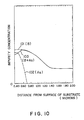
- Fig. 10 Results of measuring impurity concentration with respect to distance from the surface of the substrate of the semiconductor memory device of the third embodiment are shown in Fig. 10.
- Curve 101 shows the concentration of the p-type impurity boron
- curve 102 shows the concentration of the n-type impurity arsenic
- curve 103 shows the concentration of a p-type impurity which is a combination of boron and arsenic. It is clear from curve 103 that the concentration of p-type impurity near the surface of the semiconductor substrate 1 is controlled and reduced by arsenic.
- the threshold voltage V th of the offset transistor can be set to any desired value, facilitating current flow in the memory cell and improving access times.
- the n-type drain 6 and the p-type high-impurity-concentration region 11 are in contact with each other, the generation probability of electrons implanted into the floating gate 4 is increased and the memory cell write characteristics are improved.
- this semiconductor memory device according to the third embodiment of the present invention can be manufactured to a higher precision than those of the first and second embodiments, it can provide an even smaller semiconductor memory device.
- FIG. 8 a fourth embodiment of the present invention, shown in Fig. 8, which is the same as the third embodiment except that a portion of the isolation film 40 under the floating gate 4 and the drain 6 is formed to be thinner than the rest of the isolation film, which improves the memory cell write characteristics
- a fifth embodiment of the present invention shown in Fig. 9, which is the same as the third embodiment except that the control gate 7 and the floating gate 4 are formed in a self-aligning manner on the drain 6 side.
Landscapes
- Non-Volatile Memory (AREA)
- Semiconductor Memories (AREA)
Applications Claiming Priority (2)
| Application Number | Priority Date | Filing Date | Title |
|---|---|---|---|
| JP1137452A JPH034567A (ja) | 1989-06-01 | 1989-06-01 | 半導体記憶装置 |
| JP137452/89 | 1989-06-01 |
Publications (3)
| Publication Number | Publication Date |
|---|---|
| EP0400670A2 true EP0400670A2 (de) | 1990-12-05 |
| EP0400670A3 EP0400670A3 (de) | 1991-02-06 |
| EP0400670B1 EP0400670B1 (de) | 1994-08-24 |
Family
ID=15198940
Family Applications (1)
| Application Number | Title | Priority Date | Filing Date |
|---|---|---|---|
| EP90110472A Expired - Lifetime EP0400670B1 (de) | 1989-06-01 | 1990-06-01 | Halbleiterspeicheranordnung und Verfahren zu ihrer Herstellung |
Country Status (4)
| Country | Link |
|---|---|
| EP (1) | EP0400670B1 (de) |
| JP (1) | JPH034567A (de) |
| KR (1) | KR940002782B1 (de) |
| DE (1) | DE69011745T2 (de) |
Family Cites Families (5)
| Publication number | Priority date | Publication date | Assignee | Title |
|---|---|---|---|---|
| DE2812049C2 (de) * | 1974-09-20 | 1982-05-27 | Siemens AG, 1000 Berlin und 8000 München | n-Kanal-Speicher-FET |
| JPS54156484A (en) * | 1978-05-30 | 1979-12-10 | Nec Corp | Non-volatile semiconductor memory device |
| US4302766A (en) * | 1979-01-05 | 1981-11-24 | Texas Instruments Incorporated | Self-limiting erasable memory cell with triple level polysilicon |
| JPS59111370A (ja) * | 1982-12-16 | 1984-06-27 | Seiko Instr & Electronics Ltd | 不揮発性半導体メモリ |
| JPS6020583A (ja) * | 1983-07-14 | 1985-02-01 | Toshiba Corp | 半導体装置の製造方法 |
-
1989
- 1989-06-01 JP JP1137452A patent/JPH034567A/ja active Pending
-
1990
- 1990-05-31 KR KR1019900007993A patent/KR940002782B1/ko not_active Expired - Lifetime
- 1990-06-01 DE DE69011745T patent/DE69011745T2/de not_active Expired - Fee Related
- 1990-06-01 EP EP90110472A patent/EP0400670B1/de not_active Expired - Lifetime
Also Published As
| Publication number | Publication date |
|---|---|
| DE69011745D1 (de) | 1994-09-29 |
| KR910001874A (ko) | 1991-01-31 |
| KR940002782B1 (ko) | 1994-04-02 |
| EP0400670B1 (de) | 1994-08-24 |
| EP0400670A3 (de) | 1991-02-06 |
| DE69011745T2 (de) | 1995-02-02 |
| JPH034567A (ja) | 1991-01-10 |
Similar Documents
| Publication | Publication Date | Title |
|---|---|---|
| KR960000716B1 (ko) | 반도체장치와 그의 제조방법 | |
| US5629222A (en) | Method of forming semiconductor memory device by selectively forming an insulating film on the drain region | |
| US4268321A (en) | Method of fabricating a semiconductor device having channel stoppers | |
| US6030869A (en) | Method for fabricating nonvolatile semiconductor memory device | |
| US6207992B1 (en) | Vertical floating gate transistor with epitaxial channel | |
| JP3241330B2 (ja) | フラッシュメモリおよびその製造方法 | |
| USRE37959E1 (en) | Semiconductor integrated circuit device and method of manufacturing the same | |
| US5518944A (en) | MOS transistor and its fabricating method | |
| JPH1187707A (ja) | 半導体素子及びその製造方法 | |
| US5426327A (en) | MOS semiconductor with LDD structure having gate electrode and side spacers of polysilicon with different impurity concentrations | |
| EP0452817B1 (de) | Halbleiterbauelement mit MOS-Transistoren und Verfahren zu dessen Herstellung | |
| US4868618A (en) | Ion implanted semiconductor device | |
| JP2913817B2 (ja) | 半導体メモリの製造方法 | |
| US5243210A (en) | Semiconductor memory device and manufacturing method thereof | |
| KR100618058B1 (ko) | 전계 효과 트랜지스터를 포함하는 반도체 디바이스의 제조방법 | |
| JP2924833B2 (ja) | 不揮発性半導体記憶装置及びその製造方法 | |
| EP0400670B1 (de) | Halbleiterspeicheranordnung und Verfahren zu ihrer Herstellung | |
| JP3461998B2 (ja) | 電気的書き換え可能な半導体不揮発性メモリ装置とその製造方法 | |
| US5357133A (en) | Semiconductor memory device having improved write characteristic | |
| JP2595058B2 (ja) | 不揮発性半導体記憶装置の製造方法 | |
| JP3405664B2 (ja) | 半導体装置及びその製造方法 | |
| JP3469255B2 (ja) | 半導体装置およびその製造方法 | |
| JP2610709B2 (ja) | 不揮発性半導体記憶装置の製造法 | |
| KR100371284B1 (ko) | 플랫 셀형 반도체 메모리 장치의 제조 방법 | |
| KR100273323B1 (ko) | 반도체소자 및 그 제조방법 |
Legal Events
| Date | Code | Title | Description |
|---|---|---|---|
| PUAI | Public reference made under article 153(3) epc to a published international application that has entered the european phase |
Free format text: ORIGINAL CODE: 0009012 |
|
| 17P | Request for examination filed |
Effective date: 19900601 |
|
| AK | Designated contracting states |
Kind code of ref document: A2 Designated state(s): DE FR GB |
|
| PUAL | Search report despatched |
Free format text: ORIGINAL CODE: 0009013 |
|
| AK | Designated contracting states |
Kind code of ref document: A3 Designated state(s): DE FR GB |
|
| 17Q | First examination report despatched |
Effective date: 19930825 |
|
| GRAA | (expected) grant |
Free format text: ORIGINAL CODE: 0009210 |
|
| AK | Designated contracting states |
Kind code of ref document: B1 Designated state(s): DE FR GB |
|
| REF | Corresponds to: |
Ref document number: 69011745 Country of ref document: DE Date of ref document: 19940929 |
|
| ET | Fr: translation filed | ||
| PLBE | No opposition filed within time limit |
Free format text: ORIGINAL CODE: 0009261 |
|
| STAA | Information on the status of an ep patent application or granted ep patent |
Free format text: STATUS: NO OPPOSITION FILED WITHIN TIME LIMIT |
|
| 26N | No opposition filed | ||
| PGFP | Annual fee paid to national office [announced via postgrant information from national office to epo] |
Ref country code: GB Payment date: 19970523 Year of fee payment: 8 |
|
| PGFP | Annual fee paid to national office [announced via postgrant information from national office to epo] |
Ref country code: DE Payment date: 19970606 Year of fee payment: 8 |
|
| PG25 | Lapsed in a contracting state [announced via postgrant information from national office to epo] |
Ref country code: GB Free format text: LAPSE BECAUSE OF NON-PAYMENT OF DUE FEES Effective date: 19980601 |
|
| GBPC | Gb: european patent ceased through non-payment of renewal fee |
Effective date: 19980601 |
|
| PG25 | Lapsed in a contracting state [announced via postgrant information from national office to epo] |
Ref country code: DE Free format text: LAPSE BECAUSE OF NON-PAYMENT OF DUE FEES Effective date: 19990401 |
|
| REG | Reference to a national code |
Ref country code: FR Ref legal event code: D6 |
|
| PGFP | Annual fee paid to national office [announced via postgrant information from national office to epo] |
Ref country code: FR Payment date: 20070608 Year of fee payment: 18 |
|
| REG | Reference to a national code |
Ref country code: FR Ref legal event code: ST Effective date: 20090228 |
|
| PG25 | Lapsed in a contracting state [announced via postgrant information from national office to epo] |
Ref country code: FR Free format text: LAPSE BECAUSE OF NON-PAYMENT OF DUE FEES Effective date: 20080630 |