EP0396347A2 - Funksender, geeignet zur Kompensation einer Frequenzcharakteristik einer Antenne und/oder einer Kupplungsschaltung - Google Patents
Funksender, geeignet zur Kompensation einer Frequenzcharakteristik einer Antenne und/oder einer Kupplungsschaltung Download PDFInfo
- Publication number
- EP0396347A2 EP0396347A2 EP90304609A EP90304609A EP0396347A2 EP 0396347 A2 EP0396347 A2 EP 0396347A2 EP 90304609 A EP90304609 A EP 90304609A EP 90304609 A EP90304609 A EP 90304609A EP 0396347 A2 EP0396347 A2 EP 0396347A2
- Authority
- EP
- European Patent Office
- Prior art keywords
- signal
- frequency
- reference voltage
- temperature
- supplying
- Prior art date
- Legal status (The legal status is an assumption and is not a legal conclusion. Google has not performed a legal analysis and makes no representation as to the accuracy of the status listed.)
- Granted
Links
Images

Classifications
-
- H—ELECTRICITY
- H03—ELECTRONIC CIRCUITRY
- H03G—CONTROL OF AMPLIFICATION
- H03G3/00—Gain control in amplifiers or frequency changers
- H03G3/20—Automatic control
- H03G3/30—Automatic control in amplifiers having semiconductor devices
- H03G3/3036—Automatic control in amplifiers having semiconductor devices in high-frequency amplifiers or in frequency-changers
- H03G3/3042—Automatic control in amplifiers having semiconductor devices in high-frequency amplifiers or in frequency-changers in modulators, frequency-changers, transmitters or power amplifiers
-
- H—ELECTRICITY
- H03—ELECTRONIC CIRCUITRY
- H03F—AMPLIFIERS
- H03F1/00—Details of amplifiers with only discharge tubes, only semiconductor devices or only unspecified devices as amplifying elements
- H03F1/34—Negative-feedback-circuit arrangements with or without positive feedback
-
- H—ELECTRICITY
- H03—ELECTRONIC CIRCUITRY
- H03F—AMPLIFIERS
- H03F3/00—Amplifiers with only discharge tubes or only semiconductor devices as amplifying elements
- H03F3/20—Power amplifiers, e.g. Class B amplifiers, Class C amplifiers
- H03F3/24—Power amplifiers, e.g. Class B amplifiers, Class C amplifiers of transmitter output stages
-
- H—ELECTRICITY
- H04—ELECTRIC COMMUNICATION TECHNIQUE
- H04B—TRANSMISSION
- H04B1/00—Details of transmission systems, not covered by a single one of groups H04B3/00 - H04B13/00; Details of transmission systems not characterised by the medium used for transmission
- H04B1/02—Transmitters
- H04B1/03—Constructional details, e.g. casings, housings
- H04B1/036—Cooling arrangements
-
- H—ELECTRICITY
- H04—ELECTRIC COMMUNICATION TECHNIQUE
- H04B—TRANSMISSION
- H04B1/00—Details of transmission systems, not covered by a single one of groups H04B3/00 - H04B13/00; Details of transmission systems not characterised by the medium used for transmission
- H04B1/02—Transmitters
- H04B1/04—Circuits
- H04B2001/0408—Circuits with power amplifiers
- H04B2001/0416—Circuits with power amplifiers having gain or transmission power control
-
- H—ELECTRICITY
- H04—ELECTRIC COMMUNICATION TECHNIQUE
- H04B—TRANSMISSION
- H04B1/00—Details of transmission systems, not covered by a single one of groups H04B3/00 - H04B13/00; Details of transmission systems not characterised by the medium used for transmission
- H04B1/02—Transmitters
- H04B1/04—Circuits
- H04B2001/0408—Circuits with power amplifiers
- H04B2001/0433—Circuits with power amplifiers with linearisation using feedback
Definitions
- This invention relates to a radio transmitter for use in a mobile telephone system, a multichannel access (MCA) system, or the like to transmit an output signal in response to an input signal.
- MCA multichannel access
- a radio transmitter of the type described comprises an amplifier section which will mainly be specified by a high frequency power amplifier which forms an output stage of the amplifier section and which is connected to an antenna, although an intermediate frequency amplifier and a low frequency amplifier are also included in the amplifier section.
- the high frequency power amplifier may be considered as a combination of a variable gain high frequency power amplifier circuit and a high frequency power amplifier circuit.
- the variable gain high frequency amplifier circuit is supplied with an internal signal derived from an input signal to produce a gain controlled signal while the high frequency power amplifier circuit amplifies the gain controlled signal into the output signal.
- an output transmission power level should be preferably held substantially constant in the radio transmitter.
- an automatic level control (ALC) circuit is used in combination with the high frequency power amplifier.
- the automatic level control circuit comprises a detector supplied with the output signal to produce a detection signal, namely, a d. c. signal specifying a power level of the output signal.
- the detection signal is sent to a comparator and is compared in the comparator with a reference signal predetermined for the power level of the output signal to produce a control signal representative of a difference between the detection signal and the reference signal.
- the control signal is delivered to a power source control circuit which is connected to the variable gain high frequency power amplifier circuit and which is also connected to a power source. Supplied with the control signal, the power source control circuit controls the power source to supply controlled electric power to the variable gain high frequency power amplifier circuit and to thereby control a gain of the variable gain high frequency power amplifier circuit.
- the gain controlled signal is sent from the variable gain high frequency power amplifier circuit to the high frequency power amplifier circuit to be produced as the output signal.
- the output signal has an output level determined by the reference signal given to the comparator circuit.
- the detector is implemented by a semiconductor or a primary diode which has a temparature characteristic and that the antenna has a frequency characteristic like in a coupling circuit between the high frequency power amplifier and the antenna. Therefore, the detection signal is varied in its amplitude in dependency upon the temparature characteristic of the primary diode. In addition, the detection signal is also varied by the frequency characteristic of the antenna or the coupling circuit when frequencies are changed from one to another. Inasmuch as the level of the output signal is determined by the detection signal, as mentioned before, the output signal is varied in dependency upon the detecting signal even when the reference signal is kept constant.
- a radio transmitter to which this invention is applicable is supplied with an input signal for transmitting an output signal having a level.
- the radio transmitter comprises an amplifier section responsive to an internal signal resulting from the input signal for producing the output signal, a reference voltage supplying circuit for supplying the amplifier section with a reference voltage signal having a reference voltage to control the level of the output signal, a temperature detection circuit for detecting a temperature on a part of the radio transmitter to produce a temperature signal representative of the temperature, transmission frequency determining means for determining a transmission frequency for the input signal to produce a frequency control signal indicative of the transmission frequency, reference voltage control means supplied with the frequency control signal and the temperature signal for controlling the reference voltage signal based on the frequency control signal and the temperature signal, and internal signal supplying means connected to the amplifier section and responsive to both the frequency control signal and the input signal for supplying the internal signal to the amplifier section.
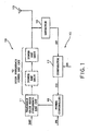
- a conventional radio transmitter comprises an amplifier section which is collectively depicted at 10 in Fig. 1 and which is specified by a variable gain high frequency amplifier circuit 11 and a high frequency power amplifier circuit 12.
- the variable gain high frequency amplifier circuit 11 is connected to a lower stage of amplifiers (not shown) and is supplied from the lower stage with an internal signal INT resulting from an input signal, such as an audio signal.
- the variable gain high frequency amplifier circuit 11 has a gain controllable in a manner to be described and produces a gain controlled signal.
- the high frequency power amplifier circuit 12 comprises a plurality of power amplifier units connected in cascade to one another and amplifies the gain controlled signal into an output signal which has a high frequency and a level corresponding to transmission power. The output signal is sent through a coupling circuit to an antenna 13 and produced as a radio signal.
- the amplifier section 10 is connected to an automatic level control (ALC) circuit 15 which comprises a detector 16 which is implemented by a semiconductor diode and which is supplied with the output signal from the high frequency power amplifier circuit 12.
- ALC automatic level control
- the detector 16 detects the output signal to produce a detection signal DT of a d. c. voltage corresponding to the transmission power of the output signal.
- the detection signal DT is sent to a comparator 17 which is supplied with a reference signal RE of a d. c. voltage from a reference signal generator (not shown in this figure).
- the reference signal RE is determined for a desired transmission power of the output signal.
- the comparator 17 compares the detection signal DT with the reference signal RE to produce a control signal CO representative of a result of comparison between the detection signal DT and the reference signal RE.
- the control signal CO is supplied to a power controller 18 which is connected to an electric power source (not shown) and which is given a source voltage PS.
- the source voltage PS is controlled by the control signal CO.
- the variable gain high frequency amplifier circuit 11 is supplied with controlled electric power from the power controller 18 to keep the transmission power of the output signal at desired transmission power.
- the transmission power of the output signal is adjusted to the desired transmission power by comparing the detection signal DT with the reference signal RE.
- the illustrated radio transmitter has disadvantages, as pointed out in the preamble of the instant specification.
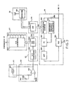
- a radio transmitter according to a preferred embodiment of this invention comprises similar parts designated by like reference numerals and symbols.
- the radio transmitter is assigned with a plurality of radio channels which have different frequencies from one another and one of which is selected as a selected channel on transmission.
- an automatic level control circuit 15′ serves to compensate for a temperature characteristic of a diode placed in the detector 16 and a frequency characteristic of the coupling circuit and the antenna 13.
- a temperature sensor 21 is located at a position adjacent to the detector 16.
- the temperature sensor 21 may be, for example, a thermistor 211 and may be attached to a housing of the amplifier section 10 or may be very close to the detector 16. At any rate, the temperature sensor 21 detects a temperature at the position and produces an electric signal related to the temperature and which appears in the form of an analog signal. In other words, a variation of the temperature brings about a variation of resistance of the thermistor 211 and varies the analog signal.
- the analog signal is varied in dependency upon the temperature and is sent to a temperature detector 22 which is formed by a differential amplifier 221 which has a positive input terminal connected to a bias circuit (not shown) and a negative input terminal connected to the thermistor 211 and a voltage source symbolized by Vcc, as shown in Fig. 3. Therefore, the thermistor 211 is connected to the differential amplifier 221 as a feedback resistor.
- the temperature detector 22 supplies a reference voltage controller 23 with an analog temperature signal TEM representative of the temperature sensed by the temperature sensor 21.
- the reference voltage controller 23 is connected to a transmission frequency controller 24 which is in turn connected to both a receiving section 25 and a transmission singal generating circuit 26.
- a reference voltage generator 27 is connected to and controlled by the reference voltage controller 23.
- the receiving section 25 comprises a receiver 251 operable in receiving a data signal as a reception data signal from another station that may be usually a base station.
- the reception data signal received through the receiver 251 includes a channel indication signal indicative of a transmission channel for the radio transmitter and is delivered to the transmission frequency controller 24 formed by a central processing unit (CPU) 241.
- CPU central processing unit
- the central processing unit 241 processes the reception data signal between the receiver 251 and the base station.
- the channel indication signal is processed by the central processing unit 241 into a frequency division signal FD which is representative of a factor of frequency division preassigned to each of the channels.
- the factor may be referred to as a division factor.
- the frequency division signal FD is made to correspond to a transmission frequency of each channel.
- the central processing unit 241 also produces a transmission channel signal TC representative of each channel. Both the frequency division signal FD and the transmission channel signal TC may be collectively referred to as a frequency control signal indicative of the transmission frequency.
- the transmission frequency controller 24 is operable to determine the transmission frequency necessary for transmitting the input signal IN.
- the frequency division signal FD and the transmission channel signal TC are sent to the transmission signal generating circuit 26 and the reference voltage controller 23, respectively.
- the transmission signal generating circuit 26 is supplied with the input signal IN, such as an audio signal, in addition to the frequency division signal FD, as shown in Fig. 2.
- the transmission signal generating circuit 26 comprises a reference frequency oscillator 261 which oscillates a reference frequency signal having a reference frequency and a programmanble counter 262 supplied with the frequency division signal FD and with a transmission frequency signal which is produced in a manner to be described later.
- the programmable counter 262 divides the transmission frequency into a frequency divided signal in accordance with the division factor represented by the frequency division signal FD.
- the frequency divided signal is delivered to a phase detector (PD) 263 together with the reference frequency signal.
- PD phase detector
- the phase detector 263 compares the frequency divided signal with the reference frequency signal to produce a difference signal representative of a phase or a frequency difference between the frequency divided signal and the reference frequency signal.
- the difference signal is usually given by a d. c. signal and is sent through a low pass filter (LPF) 264 to a voltage controlled oscillator (VCO) 265 supplied with the input signal IN.
- LPF low pass filter
- VCO voltage controlled oscillator
- the voltage controlled oscillator 265 varies an oscillation frequency in response to the difference signal sent from the phase detector 263 and obtains an oscillation frequency signal which has a frequency equal to a transmission frequency assigned to the selected channel.
- such an oscillation frequency signal is subjected by the input signal IN to frequency modulation in the voltage controlled oscillator 265 and is transmitted to the variable gain high frequency amplifier circuit 11 (Fig. 2) as a controlled input signal on one hand and to the programmable counter 262 through a capacitor 266 as the transmission frequency signal.
- the controlled input signal is delivered as the internal signal to the variable gain high frequency amplifier circuit 11. This shows that the illustrated internal signal INT is frequency modulated and has the transmission frequency assigned to the selected channel.
- the reference voltage controller 23 is operable in response to the analog temperature signal TEM and the transmission channel signal TC representative of the selected channel. More specifically, the analog temperature signal TEM is given to an analog-to-digital converter 231 and is converted into a digital temperature signal by the analog-to-digital converter 231. The digital temperature signal is supplied to a subsidiary central processing unit (abbreviated to SUBCPU) 232 along with the transmission channel signal TC.
- SUBCPU subsidiary central processing unit
- the SUBCPU 232 serves to compensate for the temperature characteristic of the detector 16 and the frequency characteristic of the antenna 13 and the coupling circuit.
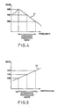
- Fig. 4 wherein an abscissa and an ordinate represent a frequency and a gain, respectively, it is assumed that the antenna 13 illustrated in Fig. 2 has a frequency characteristic, as specified by a curve 31, and that the antenna 13 is used within an available frequency band specified by an upper limit frequency and a lower limit frequency.
- the illustrated frequency chracteristic exhibits gains A dB and B dB at the lower and the upper frequency limits, respectively, as readily understood from the curve 31. Therefore, a gain difference (A - B) dB appears when the antenna 13 is driven at the lower and the upper frequency limits, unless the frequency characteristic is not compensated.
- the detector 16 has a frequency characteristic which is specified by a curve 32 and that the detector 16 has an acceptable temperature range within a first temperature T1 and a second temperature T2 lower than the first temperature T1.
- the detector 16 has the output signal levels C dB and D dB at the first and the second temperatures T1 and T2 and a level difference (C - D) dB.
- a maximum level and a minimum level of the output signal can be equivalently represented by (A + C) dB and (B + D) dB, respectively.
- the maximum and the minimum levels should be restricted to a range between + 2 dB and - 4 dB in the radio transmitter for the mobile telephone system, where 0 dB is representative of a reference level.
- the SUBCPU 232 is loaded with a first set of compensation signals which compensate for variations of gains of the detector 16 resulting from the temperature characteristic as illustrated in Fig. 5 and with a second set of compensation signals which compensate for the gain difference resulting from variations of the frequency characteristics of the antenna 13.
- the first set of the compensation signals are memorized at each temperature indicated by the digital temperature signal in an internal memory of the SUBCPU 232 while the second sets of compensation signals are held in the internal memory at every channel.
- the SUBCPU 232 Supplied with the digital temperature signal and the transmission channel signal TC, the SUBCPU 232 read a selected one of the compensation signals of the first set and a selected one of the compensation signals of the second set from the internal memory. Both the selected ones of the compensation signals are processed in an internal proccessor of the SUBCPU 232.
- the internal processor calculates, from the selected ones of the compensation signals, a reference voltage control signal RC indicative of a reference voltage which is necessary for keeping the output signal constant.
- the reference voltage control signal RC is sent to the reference voltage generator 27 to control a reference voltage RE.
- the reference voltage controller 23 serves to control the reference voltage signal RE based on the transmission channel signal TC and the analog temperature signal TEM.
- the reference voltage generator 27 comprises a digital-to-analog (D/A) converter 271 and supplies the comparator 17 (Fig. 2) with the reference voltage RE indicated by the reference voltage control signal RC.
- D/A digital-to-analog
- the reference voltage signal RE is determined by the reference voltage control signal RC dependent on the analog temperature signal TEM and the transmission channel signal TC. Accordingly, the temperature characteristic detected at a position adjacent to the detector 16 and the frequency characteristic of the antenna 13 can be preferably compensated by producing the compensation signals in consideration of the temperature and the frequency characteristics from the reference voltage controller 23.
Landscapes
- Engineering & Computer Science (AREA)
- Power Engineering (AREA)
- Computer Networks & Wireless Communication (AREA)
- Signal Processing (AREA)
- Transmitters (AREA)
Applications Claiming Priority (2)
| Application Number | Priority Date | Filing Date | Title |
|---|---|---|---|
| JP1106014A JPH02285817A (ja) | 1989-04-27 | 1989-04-27 | 無線送信機 |
| JP106014/89 | 1989-04-27 |
Publications (3)
| Publication Number | Publication Date |
|---|---|
| EP0396347A2 true EP0396347A2 (de) | 1990-11-07 |
| EP0396347A3 EP0396347A3 (de) | 1991-10-30 |
| EP0396347B1 EP0396347B1 (de) | 1994-08-31 |
Family
ID=14422807
Family Applications (1)
| Application Number | Title | Priority Date | Filing Date |
|---|---|---|---|
| EP90304609A Expired - Lifetime EP0396347B1 (de) | 1989-04-27 | 1990-04-27 | Funksender, geeignet zur Kompensation einer Frequenzcharakteristik einer Antenne und/oder einer Kupplungsschaltung |
Country Status (6)
| Country | Link |
|---|---|
| US (1) | US5081713A (de) |
| EP (1) | EP0396347B1 (de) |
| JP (1) | JPH02285817A (de) |
| AU (1) | AU630948B2 (de) |
| CA (1) | CA2015553C (de) |
| DE (1) | DE69011939T2 (de) |
Cited By (10)
| Publication number | Priority date | Publication date | Assignee | Title |
|---|---|---|---|---|
| EP0534681A3 (de) * | 1991-09-24 | 1993-06-02 | Nokia Mobile Phones Ltd. | Leistungsverstärker für ein Funktelefon |
| GB2233517B (en) * | 1989-06-26 | 1994-04-06 | Orbitel Mobile Communications | Transmitter power control for radio telephone system |
| EP0684707A1 (de) * | 1994-05-28 | 1995-11-29 | Nortel Networks Corporation | Gruppenantenne für eine zellulare Basisfunkstation mit Sendeleistungsregelung |
| WO1996033555A1 (en) * | 1995-04-21 | 1996-10-24 | Qualcomm Incorporated | Temperature compensated automatic gain control |
| FR2759219A1 (fr) * | 1997-01-31 | 1998-08-07 | Samsung Electronics Co Ltd | Procede de commande de puissance d'un signal radio en fonction de variations de frequence et de temperature dans un emetteur de recherche de personne |
| EP1160995A1 (de) * | 2000-05-29 | 2001-12-05 | Sony International (Europe) GmbH | Mobiles Endgerät für drahtloses Telekommunikationssystem |
| WO2004042946A1 (de) * | 2002-11-05 | 2004-05-21 | Siemens Aktiengesellschaft | Verfahren zum sendeleistungsabgleich bei einem mobilen kommunikationsendgerät und kommunikationsendgerät zur durchführung des verfahrens |
| WO2004051846A3 (en) * | 2002-12-04 | 2004-10-28 | Research In Motion Ltd | Gain compensation over temperature and frequency variations in wireless transceivers |
| RU2305363C2 (ru) * | 1994-12-16 | 2007-08-27 | Квэлкомм Инкорпорейтед | Способ и устройство для повышения помехозащищенности приемника |
| EP1879298A1 (de) * | 2006-07-12 | 2008-01-16 | STMicroelectronics N.V. | Verfahren und Sender/Empfänger zum Verbessern der Sendeleistung eines Signals in Breitbandsystemen, insbesondere in UWB Systemen |
Families Citing this family (42)
| Publication number | Priority date | Publication date | Assignee | Title |
|---|---|---|---|---|
| JP2936758B2 (ja) * | 1991-02-20 | 1999-08-23 | 日本電気株式会社 | 無線受信機 |
| US5287555A (en) * | 1991-07-22 | 1994-02-15 | Motorola, Inc. | Power control circuitry for a TDMA radio frequency transmitter |
| JPH0555936A (ja) * | 1991-08-21 | 1993-03-05 | Matsushita Electric Ind Co Ltd | 送信電力制御装置 |
| US5239696A (en) * | 1991-10-15 | 1993-08-24 | Sensormatic Electronics Corporation | Linear power amplifier utilizing current feedback |
| JPH05206771A (ja) * | 1992-01-30 | 1993-08-13 | Mitsubishi Electric Corp | 自動出力電力制御回路 |
| EP0573073B1 (de) * | 1992-06-05 | 1999-03-10 | Japan Radio Co., Ltd | Vorrichtung zur Sendeleistungssteuerung mit Vorspannungsstabilisierung |
| KR0182091B1 (ko) * | 1993-02-05 | 1999-05-15 | 사토 후미오 | 무선전화장치 |
| US5296821A (en) * | 1993-05-03 | 1994-03-22 | Motorola, Inc. | Method and apparatus for controlling transient responses in a power amplifier |
| US5371473A (en) * | 1993-09-10 | 1994-12-06 | Hughes Aircraft Company | Thermally stable ALC for pulsed output amplifier |
| FR2716313B1 (fr) * | 1994-02-11 | 1996-04-12 | Alcatel Mobile Comm France | Dispositif de commande de la polarisation d'un amplificateur. |
| KR0123205B1 (ko) * | 1994-12-30 | 1997-11-19 | 김주용 | 위성통신 송신기의 자동이득조절회로 |
| JPH08204587A (ja) * | 1995-01-23 | 1996-08-09 | Fujitsu Ltd | 携帯電話機 |
| JPH08274559A (ja) * | 1995-04-03 | 1996-10-18 | Oki Electric Ind Co Ltd | 出力電力制御装置 |
| US5686903A (en) * | 1995-05-19 | 1997-11-11 | Prince Corporation | Trainable RF transceiver |
| DE19521663A1 (de) * | 1995-06-14 | 1996-12-19 | Philips Patentverwaltung | Integrierter Schaltkreis mit Spannungsregelschaltung |
| JPH0946286A (ja) * | 1995-08-02 | 1997-02-14 | Fujitsu Ltd | 衛星通信地球局における送信電力制御装置 |
| US5854593A (en) * | 1996-07-26 | 1998-12-29 | Prince Corporation | Fast scan trainable transmitter |
| US5859567A (en) * | 1996-09-24 | 1999-01-12 | Motorola, Inc. | Power amplifier circuit with temperature compensating level shifter |
| US6148220A (en) * | 1997-04-25 | 2000-11-14 | Triquint Semiconductor, Inc. | Battery life extending technique for mobile wireless applications |
| RU2147159C1 (ru) * | 1997-07-11 | 2000-03-27 | Рощина Юлия Сергеевна | Двухканальная радиосеть |
| JPH11177444A (ja) * | 1997-12-15 | 1999-07-02 | Matsushita Electric Ind Co Ltd | 送信電力制御装置及び方法 |
| JP2000068958A (ja) * | 1998-08-26 | 2000-03-03 | Toshiba Corp | 無線送信装置 |
| JP3223887B2 (ja) * | 1998-09-07 | 2001-10-29 | 株式会社デンソー | 無線通信装置 |
| KR100319275B1 (ko) * | 1999-03-20 | 2002-01-09 | 윤종용 | 무선 단말기에서 온도보상에 따른 전력제어를 위한 코드 값 계산 방법 |
| US6473603B1 (en) * | 1999-04-02 | 2002-10-29 | Qualcomm, Inc. | System and method for temperature compensation of external antenna units |
| EP1249941A4 (de) * | 2000-11-13 | 2005-01-19 | Mitsubishi Electric Corp | Tragbares telefon |
| US6813476B1 (en) | 2000-11-13 | 2004-11-02 | Andrew Corporation | Method and system for compensating for atmospheric fading in a communications system |
| US7047029B1 (en) * | 2001-09-10 | 2006-05-16 | The Directv Group, Inc. | Adaptive transmission system |
| US9485010B1 (en) | 2001-09-10 | 2016-11-01 | The Directv Group, Inc. | Adaptive coding and modulation for spot beam satellite broadcast |
| US7010284B2 (en) * | 2002-11-06 | 2006-03-07 | Triquint Semiconductor, Inc. | Wireless communications device including power detector circuit coupled to sample signal at interior node of amplifier |
| US20040072554A1 (en) * | 2002-10-15 | 2004-04-15 | Triquint Semiconductor, Inc. | Automatic-bias amplifier circuit |
| US20040070454A1 (en) * | 2002-10-15 | 2004-04-15 | Triquint Semiconductor, Inc. | Continuous bias circuit and method for an amplifier |
| US7236745B2 (en) * | 2003-03-05 | 2007-06-26 | Harris Stratex Networks Operating Corporation | Transceiver power detection architecture |
| KR100498964B1 (ko) * | 2003-03-05 | 2005-07-01 | 삼성전자주식회사 | 이동단말에서의 전자파 흡수율 제어 방법 및 장치 |
| US7761067B1 (en) * | 2003-05-15 | 2010-07-20 | Marvell International Ltd. | Iterative filter circuit calibration |
| US7228114B2 (en) * | 2003-05-21 | 2007-06-05 | Harris Stratex Networks Operating Corporation | Wide dynamic range power detection scheme |
| US7653349B1 (en) | 2003-06-18 | 2010-01-26 | The Directv Group, Inc. | Adaptive return link for two-way satellite communication systems |
| KR20050032810A (ko) * | 2003-10-02 | 2005-04-08 | 삼성전자주식회사 | 자동 이득 제어 루프를 위한 온도 보상 장치 |
| US7177370B2 (en) * | 2003-12-17 | 2007-02-13 | Triquint Semiconductor, Inc. | Method and architecture for dual-mode linear and saturated power amplifier operation |
| US7164285B1 (en) * | 2005-08-12 | 2007-01-16 | Stratex Networks, Inc. | Directional power detection by quadrature sampling |
| US7825871B2 (en) * | 2007-03-19 | 2010-11-02 | Broadcom Corporation | Method and system for equalizing antenna circuit matching variations |
| KR102461147B1 (ko) * | 2015-03-16 | 2022-11-02 | 삼성전자 주식회사 | 전자 장치 및 송신 전력 제어 방법 |
Family Cites Families (11)
| Publication number | Priority date | Publication date | Assignee | Title |
|---|---|---|---|---|
| US3891926A (en) * | 1972-12-18 | 1975-06-24 | American Standard Inc | Filter module |
| US4380089A (en) * | 1980-06-16 | 1983-04-12 | Gte Products Corporation | Battery-powered transmitter including current control circuit |
| US4429285A (en) * | 1981-07-31 | 1984-01-31 | Rca Corporation | Frequency-controlled variable-gain amplifiers |
| JPS59212035A (ja) * | 1983-05-17 | 1984-11-30 | Matsushita Electric Ind Co Ltd | 送信出力制御回路 |
| JPS6041821A (ja) * | 1983-08-18 | 1985-03-05 | Nec Corp | 送信出力電力制御装置 |
| JPS6173416A (ja) * | 1984-09-19 | 1986-04-15 | Nec Corp | 自動周波数制御・自動利得制御回路 |
| JPS61121537A (ja) * | 1984-11-16 | 1986-06-09 | Nec Corp | 電力制御回路 |
| JPS63226124A (ja) * | 1986-10-29 | 1988-09-20 | Oki Electric Ind Co Ltd | 無線装置用レベル制御回路 |
| US4939786A (en) * | 1987-03-09 | 1990-07-03 | Motorola, Inc. | Adaptive thermal protection for a power amplifier by remote sense |
| US4727337A (en) * | 1987-04-24 | 1988-02-23 | Motorola, Inc. | Protection circuit for RF power amplifiers |
| JPH0752850B2 (ja) * | 1988-01-19 | 1995-06-05 | 日本電気株式会社 | 送信機 |
-
1989
- 1989-04-27 JP JP1106014A patent/JPH02285817A/ja active Pending
-
1990
- 1990-04-26 US US07/514,807 patent/US5081713A/en not_active Expired - Fee Related
- 1990-04-26 CA CA002015553A patent/CA2015553C/en not_active Expired - Fee Related
- 1990-04-27 DE DE69011939T patent/DE69011939T2/de not_active Expired - Fee Related
- 1990-04-27 EP EP90304609A patent/EP0396347B1/de not_active Expired - Lifetime
- 1990-04-27 AU AU54543/90A patent/AU630948B2/en not_active Ceased
Cited By (11)
| Publication number | Priority date | Publication date | Assignee | Title |
|---|---|---|---|---|
| GB2233517B (en) * | 1989-06-26 | 1994-04-06 | Orbitel Mobile Communications | Transmitter power control for radio telephone system |
| EP0534681A3 (de) * | 1991-09-24 | 1993-06-02 | Nokia Mobile Phones Ltd. | Leistungsverstärker für ein Funktelefon |
| EP0684707A1 (de) * | 1994-05-28 | 1995-11-29 | Nortel Networks Corporation | Gruppenantenne für eine zellulare Basisfunkstation mit Sendeleistungsregelung |
| RU2305363C2 (ru) * | 1994-12-16 | 2007-08-27 | Квэлкомм Инкорпорейтед | Способ и устройство для повышения помехозащищенности приемника |
| WO1996033555A1 (en) * | 1995-04-21 | 1996-10-24 | Qualcomm Incorporated | Temperature compensated automatic gain control |
| FR2759219A1 (fr) * | 1997-01-31 | 1998-08-07 | Samsung Electronics Co Ltd | Procede de commande de puissance d'un signal radio en fonction de variations de frequence et de temperature dans un emetteur de recherche de personne |
| EP1160995A1 (de) * | 2000-05-29 | 2001-12-05 | Sony International (Europe) GmbH | Mobiles Endgerät für drahtloses Telekommunikationssystem |
| WO2004042946A1 (de) * | 2002-11-05 | 2004-05-21 | Siemens Aktiengesellschaft | Verfahren zum sendeleistungsabgleich bei einem mobilen kommunikationsendgerät und kommunikationsendgerät zur durchführung des verfahrens |
| WO2004051846A3 (en) * | 2002-12-04 | 2004-10-28 | Research In Motion Ltd | Gain compensation over temperature and frequency variations in wireless transceivers |
| US7356102B2 (en) | 2002-12-04 | 2008-04-08 | Research In Motion Limited | Gain compensation over temperature and frequency variations in wireless transceivers |
| EP1879298A1 (de) * | 2006-07-12 | 2008-01-16 | STMicroelectronics N.V. | Verfahren und Sender/Empfänger zum Verbessern der Sendeleistung eines Signals in Breitbandsystemen, insbesondere in UWB Systemen |
Also Published As
| Publication number | Publication date |
|---|---|
| JPH02285817A (ja) | 1990-11-26 |
| EP0396347A3 (de) | 1991-10-30 |
| CA2015553A1 (en) | 1990-10-27 |
| CA2015553C (en) | 1993-04-06 |
| EP0396347B1 (de) | 1994-08-31 |
| AU5454390A (en) | 1990-11-01 |
| DE69011939D1 (de) | 1994-10-06 |
| US5081713A (en) | 1992-01-14 |
| AU630948B2 (en) | 1992-11-12 |
| DE69011939T2 (de) | 1995-02-09 |
Similar Documents
| Publication | Publication Date | Title |
|---|---|---|
| US5081713A (en) | Radio transmitter capable of compensating for a frequency characteristic of an antenna and/or a coupling circuit | |
| US5109544A (en) | Paging receiver with automatic frequency control | |
| US5603106A (en) | Adjustable transmission power control circuit | |
| EP0740422B1 (de) | Leistungssteuerungsschaltung für eine Übetragungsvorrichtung | |
| CA2074115C (en) | Output level control circuit for use in rf transmitter | |
| US5204637A (en) | Power detection technique for automatic amplifier power control | |
| US6212244B1 (en) | Fast response automatic gain control | |
| EP0534681B1 (de) | Leistungsverstärker für ein Funktelefon | |
| HU214127B (en) | Transmitter with linearized power amplifier | |
| US6788744B1 (en) | Power control circuit and transmitter | |
| US6812789B2 (en) | RF power amplifier digital gain flattening over multiband frequencies | |
| KR100411208B1 (ko) | 라디오수신기 | |
| US5263187A (en) | Automatic gain control circuit | |
| EP0698313A1 (de) | Verfahren zum einschalten eines radiosenders und radiosender | |
| US5446920A (en) | Variable transmission power type transmitter | |
| US4245350A (en) | Automatic gain control system for direct-access television receiver | |
| KR19990061211A (ko) | 자동 이득 조절과 자동 레벨 조절이 가능한 장치및 방법 | |
| US6236689B1 (en) | Device comprising a phase-locked loop, electronic apparatus comprising such a device and method of modulating the frequency of an oscillator | |
| EP0555001B1 (de) | FM Demodulatorschaltung | |
| US5714908A (en) | Power correction method and circuit | |
| JP3649579B2 (ja) | 高周波出力レベル補正回路 | |
| JPH01109908A (ja) | 周波数偏移補償回路 | |
| JPH09270715A (ja) | 送信回路とその初期設定方法 | |
| JPS59212035A (ja) | 送信出力制御回路 | |
| JPH07123065A (ja) | 時分割多重アクセス無線装置 |
Legal Events
| Date | Code | Title | Description |
|---|---|---|---|
| PUAI | Public reference made under article 153(3) epc to a published international application that has entered the european phase |
Free format text: ORIGINAL CODE: 0009012 |
|
| 17P | Request for examination filed |
Effective date: 19900517 |
|
| AK | Designated contracting states |
Kind code of ref document: A2 Designated state(s): DE FR GB NL SE |
|
| PUAL | Search report despatched |
Free format text: ORIGINAL CODE: 0009013 |
|
| AK | Designated contracting states |
Kind code of ref document: A3 Designated state(s): DE FR GB NL SE |
|
| 17Q | First examination report despatched |
Effective date: 19930514 |
|
| GRAA | (expected) grant |
Free format text: ORIGINAL CODE: 0009210 |
|
| AK | Designated contracting states |
Kind code of ref document: B1 Designated state(s): DE FR GB NL SE |
|
| REF | Corresponds to: |
Ref document number: 69011939 Country of ref document: DE Date of ref document: 19941006 |
|
| ET | Fr: translation filed | ||
| RIN2 | Information on inventor provided after grant (corrected) |
Free format text: MIYAZAKI, SHINICHI |
|
| EAL | Se: european patent in force in sweden |
Ref document number: 90304609.2 |
|
| NLXE | Nl: other communications concerning ep-patents (part 3 heading xe) |
Free format text: PAT.BUL.22/94 CORR.:MIYAZAKI, SHINICHI TE TOKIO, JAPAN |
|
| PLBE | No opposition filed within time limit |
Free format text: ORIGINAL CODE: 0009261 |
|
| STAA | Information on the status of an ep patent application or granted ep patent |
Free format text: STATUS: NO OPPOSITION FILED WITHIN TIME LIMIT |
|
| 26N | No opposition filed | ||
| PGFP | Annual fee paid to national office [announced via postgrant information from national office to epo] |
Ref country code: SE Payment date: 19970414 Year of fee payment: 8 |
|
| PGFP | Annual fee paid to national office [announced via postgrant information from national office to epo] |
Ref country code: NL Payment date: 19970430 Year of fee payment: 8 |
|
| PG25 | Lapsed in a contracting state [announced via postgrant information from national office to epo] |
Ref country code: SE Free format text: LAPSE BECAUSE OF NON-PAYMENT OF DUE FEES Effective date: 19980428 |
|
| PG25 | Lapsed in a contracting state [announced via postgrant information from national office to epo] |
Ref country code: NL Free format text: LAPSE BECAUSE OF NON-PAYMENT OF DUE FEES Effective date: 19981101 |
|
| NLV4 | Nl: lapsed or anulled due to non-payment of the annual fee |
Effective date: 19981101 |
|
| EUG | Se: european patent has lapsed |
Ref document number: 90304609.2 |
|
| REG | Reference to a national code |
Ref country code: GB Ref legal event code: IF02 |
|
| PGFP | Annual fee paid to national office [announced via postgrant information from national office to epo] |
Ref country code: DE Payment date: 20020502 Year of fee payment: 13 |
|
| PGFP | Annual fee paid to national office [announced via postgrant information from national office to epo] |
Ref country code: FR Payment date: 20030408 Year of fee payment: 14 |
|
| PGFP | Annual fee paid to national office [announced via postgrant information from national office to epo] |
Ref country code: GB Payment date: 20030423 Year of fee payment: 14 |
|
| PG25 | Lapsed in a contracting state [announced via postgrant information from national office to epo] |
Ref country code: DE Free format text: LAPSE BECAUSE OF NON-PAYMENT OF DUE FEES Effective date: 20031101 |
|
| PG25 | Lapsed in a contracting state [announced via postgrant information from national office to epo] |
Ref country code: GB Free format text: LAPSE BECAUSE OF NON-PAYMENT OF DUE FEES Effective date: 20040427 |
|
| GBPC | Gb: european patent ceased through non-payment of renewal fee |
Effective date: 20040427 |
|
| PG25 | Lapsed in a contracting state [announced via postgrant information from national office to epo] |
Ref country code: FR Free format text: LAPSE BECAUSE OF NON-PAYMENT OF DUE FEES Effective date: 20041231 |
|
| REG | Reference to a national code |
Ref country code: FR Ref legal event code: ST |