EP0393251A1 - Système connexion modulaire, avec connecteurs montés en surface à haute densité des éléments de contact - Google Patents
Système connexion modulaire, avec connecteurs montés en surface à haute densité des éléments de contact Download PDFInfo
- Publication number
- EP0393251A1 EP0393251A1 EP89200986A EP89200986A EP0393251A1 EP 0393251 A1 EP0393251 A1 EP 0393251A1 EP 89200986 A EP89200986 A EP 89200986A EP 89200986 A EP89200986 A EP 89200986A EP 0393251 A1 EP0393251 A1 EP 0393251A1
- Authority
- EP
- European Patent Office
- Prior art keywords
- contact
- connector
- circuit board
- printed circuit
- housing
- Prior art date
- Legal status (The legal status is an assumption and is not a legal conclusion. Google has not performed a legal analysis and makes no representation as to the accuracy of the status listed.)
- Granted
Links
Images


Classifications
-
- H—ELECTRICITY
- H01—ELECTRIC ELEMENTS
- H01R—ELECTRICALLY-CONDUCTIVE CONNECTIONS; STRUCTURAL ASSOCIATIONS OF A PLURALITY OF MUTUALLY-INSULATED ELECTRICAL CONNECTING ELEMENTS; COUPLING DEVICES; CURRENT COLLECTORS
- H01R24/00—Two-part coupling devices, or either of their cooperating parts, characterised by their overall structure
- H01R24/38—Two-part coupling devices, or either of their cooperating parts, characterised by their overall structure having concentrically or coaxially arranged contacts
- H01R24/40—Two-part coupling devices, or either of their cooperating parts, characterised by their overall structure having concentrically or coaxially arranged contacts specially adapted for high frequency
- H01R24/50—Two-part coupling devices, or either of their cooperating parts, characterised by their overall structure having concentrically or coaxially arranged contacts specially adapted for high frequency mounted on a PCB [Printed Circuit Board]
-
- H—ELECTRICITY
- H01—ELECTRIC ELEMENTS
- H01R—ELECTRICALLY-CONDUCTIVE CONNECTIONS; STRUCTURAL ASSOCIATIONS OF A PLURALITY OF MUTUALLY-INSULATED ELECTRICAL CONNECTING ELEMENTS; COUPLING DEVICES; CURRENT COLLECTORS
- H01R12/00—Structural associations of a plurality of mutually-insulated electrical connecting elements, specially adapted for printed circuits, e.g. printed circuit boards [PCB], flat or ribbon cables, or like generally planar structures, e.g. terminal strips, terminal blocks; Coupling devices specially adapted for printed circuits, flat or ribbon cables, or like generally planar structures; Terminals specially adapted for contact with, or insertion into, printed circuits, flat or ribbon cables, or like generally planar structures
- H01R12/50—Fixed connections
- H01R12/51—Fixed connections for rigid printed circuits or like structures
- H01R12/55—Fixed connections for rigid printed circuits or like structures characterised by the terminals
- H01R12/57—Fixed connections for rigid printed circuits or like structures characterised by the terminals surface mounting terminals
-
- H—ELECTRICITY
- H01—ELECTRIC ELEMENTS
- H01R—ELECTRICALLY-CONDUCTIVE CONNECTIONS; STRUCTURAL ASSOCIATIONS OF A PLURALITY OF MUTUALLY-INSULATED ELECTRICAL CONNECTING ELEMENTS; COUPLING DEVICES; CURRENT COLLECTORS
- H01R12/00—Structural associations of a plurality of mutually-insulated electrical connecting elements, specially adapted for printed circuits, e.g. printed circuit boards [PCB], flat or ribbon cables, or like generally planar structures, e.g. terminal strips, terminal blocks; Coupling devices specially adapted for printed circuits, flat or ribbon cables, or like generally planar structures; Terminals specially adapted for contact with, or insertion into, printed circuits, flat or ribbon cables, or like generally planar structures
- H01R12/70—Coupling devices
- H01R12/71—Coupling devices for rigid printing circuits or like structures
- H01R12/72—Coupling devices for rigid printing circuits or like structures coupling with the edge of the rigid printed circuits or like structures
- H01R12/722—Coupling devices for rigid printing circuits or like structures coupling with the edge of the rigid printed circuits or like structures coupling devices mounted on the edge of the printed circuits
-
- H—ELECTRICITY
- H05—ELECTRIC TECHNIQUES NOT OTHERWISE PROVIDED FOR
- H05K—PRINTED CIRCUITS; CASINGS OR CONSTRUCTIONAL DETAILS OF ELECTRIC APPARATUS; MANUFACTURE OF ASSEMBLAGES OF ELECTRICAL COMPONENTS
- H05K3/00—Apparatus or processes for manufacturing printed circuits
- H05K3/30—Assembling printed circuits with electric components, e.g. with resistor
- H05K3/32—Assembling printed circuits with electric components, e.g. with resistor electrically connecting electric components or wires to printed circuits
- H05K3/34—Assembling printed circuits with electric components, e.g. with resistor electrically connecting electric components or wires to printed circuits by soldering
- H05K3/3405—Edge mounted components, e.g. terminals
-
- H—ELECTRICITY
- H01—ELECTRIC ELEMENTS
- H01R—ELECTRICALLY-CONDUCTIVE CONNECTIONS; STRUCTURAL ASSOCIATIONS OF A PLURALITY OF MUTUALLY-INSULATED ELECTRICAL CONNECTING ELEMENTS; COUPLING DEVICES; CURRENT COLLECTORS
- H01R2103/00—Two poles
-
- H—ELECTRICITY
- H05—ELECTRIC TECHNIQUES NOT OTHERWISE PROVIDED FOR
- H05K—PRINTED CIRCUITS; CASINGS OR CONSTRUCTIONAL DETAILS OF ELECTRIC APPARATUS; MANUFACTURE OF ASSEMBLAGES OF ELECTRICAL COMPONENTS
- H05K2201/00—Indexing scheme relating to printed circuits covered by H05K1/00
- H05K2201/10—Details of components or other objects attached to or integrated in a printed circuit board
- H05K2201/10007—Types of components
- H05K2201/10189—Non-printed connector
Definitions
- This invention relates to a modular connector system and in particular to a system wherein connector modules with high contact density are surface mounted to printed circuit boards.
- a connector module generally comprises a housing of electrically insulative material which accommodates a plurality of contact elements or terminals arranged in rows and columns.
- the contact elements have a base section and a contact end and connecting end extending from opposite ends of the base section.
- the connecting ends project outside one side of the housing and are connected to a printed circuit board.
- the contact element density of a connector cannot be increased simply placing the contact elements closer together or by forming several rows of contact elements located above one one another. Generally, this results in an undesirable mutual electrical interference between the contact elements, essentially as a consequence of capacitive couplings between them. Furthermore, it is not possible in a connector to use an unlimited number of rows located above each other because contact elements with very long connecting ends to the printed circuit board will increase problems due to the occurrence of undesired inductive couplings and the circuit becomes more sensitive to electromagnetic noise signals.
- Figure 1 of this patent shows a contact element in which a tongue-shaped solder end extends from a U-shaped base section and projects, after mounting of the contact element, outside the connector for connection to a printed circuit board.
- Figure 8 of this patent the connecting ends of contact elements located in a column above each other are connected, by soldering, one behind the other to the printed circuit board in the direction facing away from the housing.
- the uppermost connecting end as viewed from the printed circuit board, is relatively long and has therefore a large leakage inductance.
- the present invention therefore has as one of its objects providing a connector module with a high contact element density in which the above-mentioned disadvantages of the prior art are largely overcome. This is accomplished by mutually displacing the connecting ends of adjoining contact elements in the same column in the direction of the row, i.e., in the longitudinal direction of the connector housing. This displacement may be accomplished by offsetting the connecting ends to extend within the side edge of the base section.
- the connecting ends of the contact elements can be connected to a printed circuit board next to each other in a column, in a row direction or in a longitudinal direction as viewed from the housing. This minimizes the length of the connecting ends of the contact elements which are further away from the board and, therefore, results in corresponding reduction in the sensitivity to electromagnetic interference.
- the connector module of the present invention is particularly suitable as an edge connector for connection to a printed circuit board.
- the connector of the invention may in one embodiment have connecting ends which are inclined in the direction of an imaginary plane extending transversely to and in the longitudinal direction of side of of the housing for connecting the printed circuit board which is to be mounted in this plane on one or both sides.
- the connecting ends possess, near their free extremities, a flat portion for surface mounting to a printed circuit board according to the above.
- the free extremities of the connecting ends are bent backwards relative to the imaginary plane in order to form a funnel which can readily receive the printed circuit board.
- a still further embodiment of the connector according to the invention has two rows of contact elements which are located on either side of the imaginary plane.
- the base section of the contact elements has to be designed so as to be flat, as shown in Figure 3 of the above U.S. Patent No. 4,607,907.
- a further embodiment of the connector according to the present invention has contact elements which are arranged in four rows and the connecting ends are designed as flat connecting tongues which form an integral part with the base section. The respective connecting tongues are located near an edge of the base section.
- the free extremities of the connecting tongues of adjoining contact elements in a column extend on one side of the imaginary plane over various distances from the housing in the plug-on direction of the connector.
- the respective connecting surfaces on the printed circuit board may also be arranged mutually displaced with respect to the edge of the board at the plug-on side.
- This is in contrast to connecting surfaces which must be arranged next to each other as in the case of connectors with terminals having connecting ends which terminate at the same distances.
- the above-mentioned displaced arrangement of the connecting surfaces permits not only wider connecting surfaces, wider connecting ends and/or wider flat parts of the contact elements for connection thereof with the consequent associated greater mechanical strength, but inter alia, also increases the reliability during soldering of the connecting ends.
- the connecting surfaces are separated from one another by a relatively large distance, the risk of undesirable connections is thereby smaller than in the case of surfaces arranged next to one another.
- the contact elements of the invention are also fairly simple to manufacture.
- the contact elements have two separate connecting tongues, one of which is removed in the final assembled state in order to achieve the mutual displacement of the connecting ends of the adjoining contact elements.
- the displaced arrangement of the connecting ends in the longitudinal direction of the connector housing has the further advantage that the flat portions of the respective connecting ends do not slide during mounting over their respective connecting surface on the printed circuit board. This prevents soldering paste or electrically conductive adhesive which may be present on these connecting surfaces from being removed during fitting of the connector on the printed circuit board.
- a still further embodiment of a connector module according to the invention may have a housing wall thickness on the end faces which is smaller than or equal to half the pitch distance between the contact elements, arranged so as to adjoin each other in a row.
- the connectors designed in this way can be mounted with the end edges up against each other without losing space for a column of contact elements. This is particularly advantageous in the case of printed circuit boards requiring connectors with a high contact element density.
- a further embodiment of the connector module according to the present invention has formed in the housing on the side from which the connecting ends of the contact elements project outward at least one row of openings extending in the longitudinal direction of the housing and adjacent to a side wall thereof. These openings interact with a protective plate which is provided near at least one of its edges with teeth for insertion in at least one row of openings in the housing of the connector in a manner such that, in the assembled state, the protective plate extends parallel to the aforenoted imaginary plane.
- a preferred embodiment of the protective plate has teeth which are formed on an elongated rail of electrically insulating material.
- the rail is disposed near an edge of the protective plate and the teeth are situated at a distance from the surface of the protective plate.
- a high contact density is achieved with the connector module according to the invention and in particular with the connector having four rows.
- the connector comprises a housing of electrically insulating material with several contact elements arranged in rows and columns and having contact ends and a connecting end, constructed as a plug-on contact, of electrically conducting material for connecting a conductor (i.e. core) of the ribbon cable.
- the cable connector has several open channels extending in the column direction of the contact elements, from one side of the housing to the other, for receiving the conductors of the ribbon cable from one side, only one plug-on contact being located in each channel and the contact elements situated adjacent to the other side of the 4 housing being arranged in a manner such that, if two cable connectors are positioned with the other sides situated opposite each other, the respective contact elements in one and the same column are separated from each other by a distance of at least one position.
- the through channels make easy assembly of the ribbon cable possible.
- the displaced sitting of the contact elements achieves the result that, the ends, lying opposite each other, of the individual cores of the ribbon cables connected to the respective cable connectors always have a mutual distance equal to the width of one row. Accordingly, there is no danger of the conductors situated opposite each other being able to make electrical contact with each other, assuming that the end to be connected of each ribbon cable is finished in accordance with the position of the contact elements.
- a preferred embodiment of the cable connector according to the invention comprises two rows and an even number of columns.
- the plug-on contacts situated in adjacent channels are each arranged in another row.
- the external dimensions of the cable connector are such that no space is lost for one or more of the contact elements.
- two or more cable connectors may be connected directly adjoining, for example, a four-row connector according to the invention.
- the present invention further relates to a contact element of electrically conducting material and, in particular, one for use in connector or cable connector modules such as described above.
- the contact element has a flat base section and a contact end having two resilient contact fingers projecting from the flat base section with contact surfaces located at the fee ends thereof.
- the contact iingers extend symmetrically relative to the center line in the longitudinal direction of the contact element and, at the extremity connected to the flat base section, are bent out of the plane of the base section over a portion of their length in opposite directions.
- the two contact fingers are bent towards each other again at the end of this portion in a manner such that the contact surfaces are located opposite each other.
- the invention also relates to a power connector module comprising at least one contact socket or contact pin, surrounded by a housing, with an elongated connecting end of electrically conducting material for connecting the power connector to a printed circuit board.
- the connecting end is provided with a slot-shaped opening in which the printed circuit board can be received for connecting the power connector to one or both flat sides thereof by surface mounting.
- Power connectors of this type are used, in particular, for connecting supply lines.
- the invention furthermore relates to a coaxial connector module comprising at least one outermost and innermost contact socket or innermost contact pin, mutually electrically insulated and surrounded by a housing, and having connecting ends of electrically conducting material for connecting the coaxial connector to a printed circuit board.
- the outermost contact socket has a connecting end for connecting it to one side of the printed circuit board and the innermost contact socket or innermost contact pin has a connecting end for connecting it to the other side of the printed circuit board by the surface mounting.
- printed circuit board which is also commonly referred to as “printing wiring board”
- printing wiring board is understood as meaning, in general, substrates with conducting tracks and thus, for example, also substrates of liquid crystal displays.
- the invention also relates to a contact element with a flat base section for use in the connector or cable connector modules according to the invention.
- the contact end of the contact element is a contact pin projecting from the base section.
- a connector or cable connector modules according to the invention may be provided with several such contact elements.
- the contact pin of at least one of the contact elements in a column has an unequal length relative to the contact pins of the other contact elements in the same column.
- Figure 1 shows diagrammatically in perspective two embodiments of contact elements of electrically conducting material, located on either side of a printed circuit board 1,2 with connecting ends arranged for surface mounting to the board.
- the printed circuit board 1,2 is essentially located in the middle between four rows of contact elements arranged in columns, only two elements in each row being shown in Figure 1.
- contact lingers 7,8 extend in one direction and a flat connecting tongue 5 extends in the other, opposite direction from a flat base section 6.
- the connecting tongues 5 of the various contact elements are arranged so that they adjoin each other in a column and are connected to the printed circuit board 1,2 so as to be mutually displaced in the longitudinal direction.
- the connecting tongues are inclined in the direction of the printed circuit board 1,2 and extend from an edge of the flat base section 3 or 6.
- the connecting tongues 5 have, near their free extremity, a flat portion 9 located parallel to the board 1,2 for surface mounting to connecting surfaces 10,11 on the printed wiring board 1,2.
- Connecting surfaces 10 are arranged in one row nearer to the edge at either side of the board while connecting surfaces 11 are also arranged in a row further from the edge of each side of the board.
- the contact elements of the innermost rows are situated directly adjacent to the printed circuit board 1,2, the flat portion 9 of these contacts units are situated virtually in the plane clamped by the respective flat base sections 3,6.
- the flat portion 9 of the contact elements actually merges smoothly into the connecting tongue 5 of these contact elements.
- the connecting tongues 5 do not always have to be flat, however, but may, for example, also have a round, elliptical or polygonal crosssection and/or may be narrower than the flat portion 9 for connecting to the connecting surfaces 10,11 of the printed circuit board 1,2.
- the connecting tongues 5 further have a free extremity 12 which is bent backwards at an angle relative to the printed circuit board 1,2.
- connection tongues 5 located on each side of the printed circuit board 1,2 are connected to connecting surfaces 10,11 lying displaced in the plug-on direction of the connector, transversely to the board 1,2.
- surfaces 10 are arranged in 6 rows nearer the edge of each side while surfaces 11 are also arranged in a row further from each edge.
- the center elements of the innermost rows described above contact surfaces 10.
- the outer row of contact elements elements have connecting tongues more inclined to their respective base sections 3,6 and the board 1,2 and contact surfaces 11 on either side of the board.
- Wider connecting surfaces or wider connecting tongues 5 and/or wider flat sections 9 thereof mean not only a mechanically stronger connection to the printed circuit board, but also a more reliable solder joints. Because the soldered surfaces are relatively far removed from each other in the case of the displaced arrangement shown of the connecting surfaces 10,11, the risk of undesirable solder connections is in this case less than in the case of connecting surfaces 10,11 situated next to each other in a row. As the pitch distance of the contact elements decreases, there is an increasingly greater advantage in the displaced arrangement of the connecting surfaces.
- the connecting tongues 5 of the respective contact elements extend in each case from the edge of the respective flat base section 3,6 and form an integral part therewith. It will be clear that the connecting tongues 5 can also be arranged so as to be displaced relative to the edge of each flat base section 3,6 and can also extend, for example, from the center thereof. Contact elements with connecting ends mating sideways and in the middle of the base section can then be used, as shown in Figure 1, for connectors consisting of six rows of contact elements, i.e., three on either side of the board 1,2.
- the connecting ends can be arranged in such a way that, for example, three rows of contact elements can be located with the respective connecting ends on one side of the printed circuit board 1,2 and, for example, only one or two rows on the other side, according to the positioning of the connecting ends.
- the contact elements be connected on both sides of the printed wiring board, although such a symmetrical arrangement is preferable in the case of connectors with a large number of contact elements because of the warping of the board and the risk of tearing of the thin conducting racks on the board.
- the flat portions 9 alone slide over only those connecting surfaces 10,11 on which they are connected so that any solder or adhesive paste present on these connecting surfaces is not damaged or pushed away by a connecting tongue other than that to be connected to a corresponding connecting surface sliding over it.
- the contact surfaces 10,11 may, of course, have another suitable shape for connecting the contact elements which differs from the rectangular shape shown.
- Figure 2 shows diagrammatically in perspective and impartially cut-away form two embodiments of a connector module according to the invention in which the contact elements of Figure 1 are used.
- the contact pins are fastened in the rear wall 14 of the housing 13 which is arranged against the edge of the board.
- the side walls 15,16 of the connector 13 have a mutual distance such that a connector 17 shown on the left-hand side of Figure 2 can, for example, be arranged therebetween with the contract fingers 7,8 making electrical contact with the contact pins 4.
- the contact elements shown on the left-hand side of Figure 1 are fixed in the rear wall 22 of this connector 17.
- the narrow edges of the flat base section 3,6 of the contact elements, arranged so as to adjoin each other in a row, are located opposite each other while the broad surfaces of the flat base sections 3,6 of the contact elements, arranged so as to adjoin each other in a column, are located opposite each other.
- the capacitive interference between two adjoining contact elements is directly proportional to the surface of the broad sections lying opposite each other and is inversely proportional to the distance therebetween while the distance between the contact elements arranged in Figure 2 so as to adjoin each other in a row is relatively small, thus implying a large capacitive coupling therebetween the fact that the narrow edges of the flat base sections 3,6 are the surfaces opposite each other results in relatively small capacitance.
- the broad surface of the base sections 3,6 are located opposite each other is in fact now relatively large but because the distance therebetween as a result of the illustrated sitting of the contact elements is also relatively large, the resulting capacitive interference remains small.
- the connecting tongues 5 themselves may be connected, as shown, directly to the printed circuit board 1,2 and may be relatively short, which is an advantage in connection with the sensitivity to electro-magnetic interference and inductive couplings between the respective connecting tongues.
- the usual minimum pitch distance of 2.54 mm between the contact elements adjoining each other in rows and columns can then be advantageously reduced to 2 mm or less. This results in a considerable space saving, in particular in the case of connectors with a large number of contact elements, thus achieving a higher contact element density in a connector of given dimensions.
- Figure 3 shows, on an enlarged scale, a partial section along the Line III-III in the longitudinal direction of the connector 17 shown in Figure 2 and connected to the printed circuit board 2.
- This connector has, on the front side 18 facing away from the printed wiring board, openings 19 which expand towards the outside and in which a contact pin can be inserted for contacting the resilient contact fingers 7,8 extending from the flat base section 6.
- Figure 3 also shows that the contact elements can all be manufactured in the same way; namely, by manufacturing them with the two connecting tongues 5 connected to a carrier strip 21. During assembly of the connector, one connecting tongue is subsequent removed, the other connecting tongue is brought to the required length and the flat section 9 and the bend 12 are formed. It will be clear that such a universal contact element offers great advantages during assembly of a mass-produced article such as a connector.
- Figure 4 shows, on an enlarged scale, the cross-section through the connector 17 shown in Figure 2.
- the contact fingers 7,8 are bent, on the extremity connected to the base section 6, over a section of their length in opposite direction out of the plane of the base section 6.
- the two contact fingers 7,8 are bent towards each other again at the end of this section and the contact surfaces 23 are located at the free extremities lying above each other (see also Figure 3).
- raised portions and guides may be fitted in the channel 20 of the connector 17.
- the sections of the contact fingers 7,8 bent out of the plane of the base section 6 may rest against these raised portions and guides.
- Figure 5 shows, on an enlarged scale, a view facing the rear wall 22 of the connector 17 in Figure 2 in which the connecting tongues 5 project to the outside.
- the left-hand two rows are provided with contact elements in the drawing.
- the flat base sections 6 of the contact elements are clamped in slits 24 in the rear wall 22 of the connector.
- a section along the line V-V in Figure 4 is shown for one contact element, the hatched sections being the contact surfaces 23 of the contact iingers 7,8 (see also Figure 1).
- the contact surfaces 23 may be made flat or curved.
- the slits 24 for receiving the flat base sections 6 or 3 are situated in the center of the channels 20.
- the capacitance between adjacent contact elements has the same low value over the whole connector.
- This arrangement of contact elements is possible as a consequence of the fact that the contact fingers 7,8 are bent in the opposite direction out of the plane of the flat base section 6.
- the contact pins 4 in a column of the connector 13 shown on the right-hand side of Figure 2 may be of mutually different lengths (not shown).
- the longest contact pin for example, can be used for grounding purposes, the next shortest contact pin for providing the supply voltage and the other still shorter contact pins can, for example, be used for signal paths. These last mentioned contact pins may be of equal length.
- contact is first made with the ground contact pin, then with the supply contact pin and then with the signal contact pins. This advantageously ensures that the apparatus is always connected first to ground so that any fault currents as a result of short circuits or static charge and the like can flow away directly.
- the contact pins 4 may also have a section differing from the rectangular shape shown, such as, for example, a truncated elliptical form.
- Figure 6 shows a row of the connector modules 131-134, 171-174 of varying lengths constructed according to the invention. As is clearly visible, long rows of connector modules can be formed without loss of space for a contact element. To permit this, however, the wall thickness at the end faces of the connectors 13,17 shown in Figure 2 is smaller than or equal to half the pitch; that is to say, the distance between two adjoining contact elements in a row.
- the contact elements may advantageously be made of flat spring material.
- the housing of the connector may be made of thermoplastic polyester resin, such as "Rynite” FR-530 produced by the Du Pont Company. This material makes possible to construct a connector with a smaller wall thickeners which is resistant to the higher temperatures which may arise in vapor phase soldering (VPS) while maintaining mechanical strength and breaking resistance.
- VPS vapor phase soldering
- Figure 7 shows, in perspective, a partial diagram of two connector modules 17 which are connected mounted one above the other to a printed wiring board 2.
- a protective plate 27 is shown on the right-hand side of the connectors 17, viewed from the contact openings thereof.
- the protective plate 27 is located parallel to the right-hand sidewalls 25 of the connectors 17 at a distance above the printed circuit board 2.
- the portion of the protective plate 27 situated opposite the right-hand sidewall 25 extends beyond the connectors 17 and is shown partially cut-away.
- the protective 27 is further provided with an elongated rail 29.
- a similar protective plate 28 having rail 29 is shown parallel to the left-hand sidewall 26 of the connectors 17.
- the rail 29 is provided with teeth 30 projecting parallel to the plane of the respective protective plates 27,28 in the direction of the front 18 of the connector 17.
- the teeth 30 are mutually insulated electrically relative to each other and relative to the protective plate.
- the rail 29 can advantageously be made of a plastic by means of, for example, an injection moulding technique.
- the teeth 30 have to be inserted in the connectors 17 on the rear side 22.
- the mutual distance between the teeth 30 and the dimensions thereof are such that they can be received adjacent to the base sections 6 of the contact elements of the outermost rows of the connectors 17 in the channels 20 shown in Figure 4.
- Other suitable openings for receiving the teeth 30 may also be disposed in the rear wall 22 in a manner such that in the assembled state the protective plate extends parallel to the printed circuit board, as shown in Figure 7.
- the protective plates 27,28 may be manufactured from a suitable plastic material.
- the protective plates may be manufactured from electrically conductive material or form, for example, plastic with an electrically conductive layer applied thereupon.
- the protective plates can also comprise several plate sections connected together, if necessary.
- the protective plates it is not necessary for the protective plates to extend over their entire surface in the same plane but they may also be designed such that they partially extend at a greater or partially at a smaller distance above the printed wiring board 2.
- positioning projections 33 which may be broken away are formed on the rail 29.
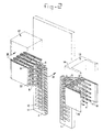
- Figure 8 shows a printed circuit board 2 with connectors according to the invention fitted on opposite sides.
- Several protective plates 27,28 of different dimensions are mounted on the two flat sides of the printed wiring board 2. Openings 34 are formed in the protective plates 27 in a manner such that the protective plates can be mechanically connected to the printed circuit board 2 by means of, for example, screws and spacers. This results in the desired strong mechanical connection between the diverse connectors and the printed wiring board.
- the protective plates are provided with ribs 35 extending in the longitudinal direction of the connectors 13. This increases the mechanical stability of the protective plates and prevents the protective plates from being bent during rough contact of the connectors 13. It should be clear that ribs 35 extending in the transverse direction (not shown) across the protective plates may also be provided with the same object.
- FIG 9 two cable connector modules having a housing 36 with two rows of contact openings located opposite each other at a distance are shown diagrammatically in perspective on an enlarged scale.
- the ribbon cables 37 has conductors disposed opposite each other in the open channels 338 of the respective cable connectors.
- the channels extend in the column direction of the contact elements from one side of the housing to the other to prevent these conductors making undesired electrical contact with each other, the contact elements of the cable connectors 36 are so arranged that only one connecting end of a contact element is situated in each channel 38 so that, if two ribbon cable connectors are positioned opposite each other, the respective contact elements in the same column are separated from each other over at least a distance of one position.
- end of a ribbon cable 37 to be received in a cable connector has a course corresponding to the siting of the connecting ends of the contact elements so that after assembly of the ribbon cable, the conductors of the contacting extremities do not project beyond the housing 36, the ends of the contacted conductors will then not touch each other when the cable connectors are mounted opposite each other.
- the contact elements can, of course, be arranged in different ways. For example, adjoining contact elements of a two- row cable connector with an even number of columns can each be located in a different row with the end of the ribbon cable 37 to be received in the cable connector having a castellated course.
- the contact elements may have a flat base section from which contact iingers or a contact pin extend with the connecting end being designed as a plug-on contact (not shown).
- the pitch distance between the contact elements is preferably 2 mm.
- projections 39 which can be broken away, are attached to avoid erroneous contacting.
- Figure 10 shows diagrammatically in perspective and in partially cut-away view, power connectors 40,41 and coaxial connectors 46,47 for connecting by surface mounting feed cables and coaxial cables to a printed circuit board. Connectors previously described are less suitable for connecting feed cables carrying a relatively large current.
- the unipolar power connector 40 is essentially constructed from a contact socket 42 of electrically conducting material having a spring-loaded contact end for receiving a contact pin and an elongated socket-shaped connecting end 43 for connection to a printed wiring board.
- the power connector 41 has a pin-shaped contact end 52 and a similar socket-shaped connecting end 43.
- the elongate connecting end 43 is provided, according to the invention, with a slot-shaped recess 45 in which the printed circuit board 2 may be received so that the connecting end 43 can be connected to the printed circuit board 2 at the two opposite flat sides thereof.
- coaxial connectors 46,47 are used in practice. These connectors have an elongated outermost contact of socket 48 and innermost contact socket 49 which are electrically insulated from each other and respectively an outermost contact socket and an innermost contact pin (not shown) of electrically conducting material.
- a part of the connecting end of the outermost contact socket 48 is removed from the circumference so that the remaining, virtually semicylindrical connecting end 50 can be connected to one side of the printed circuit board 2.
- Part of the jacket of the innermost contact socket 49, or the innermost contact pin, is removed so that the remaining connecting tongue 51 can be connected to the other side of the printed circuit board 2.
- the connectors designed in this manner possess sufficient mechanical stability and a sufficiently large contact surface so that reliable and mechanically stable connections with a printed circuit board can be made by surface mounting technique.
- the connector modules may include optoelectronic connectors connected to optical fiber cables, shielded connectors, to locking means or so called polarity indicators to prevent incorrect connection of the connector modules, etc., all without deviating from the scope and the concept of the invention.
Landscapes
- Engineering & Computer Science (AREA)
- Manufacturing & Machinery (AREA)
- Microelectronics & Electronic Packaging (AREA)
- Coupling Device And Connection With Printed Circuit (AREA)
- Multi-Conductor Connections (AREA)
- Optical Modulation, Optical Deflection, Nonlinear Optics, Optical Demodulation, Optical Logic Elements (AREA)
Priority Applications (10)
| Application Number | Priority Date | Filing Date | Title |
|---|---|---|---|
| SG1996008634A SG55167A1 (en) | 1989-04-17 | 1989-04-17 | Coaxial connector for a connection to a printed circuit board |
| EP94203024A EP0643448B1 (fr) | 1989-04-17 | 1989-04-17 | Connecteur coaxial pour la connexion de plaquettes de circuits imprimés |
| EP94203023A EP0643443A1 (fr) | 1989-04-17 | 1989-04-17 | Connecteur de puissance pour la connexion de plaquettes de circuits imprimés |
| EP89200986A EP0393251B1 (fr) | 1989-04-17 | 1989-04-17 | Système connexion modulaire, avec connecteurs montés en surface à haute densité des éléments de contact |
| DE68923361T DE68923361T2 (de) | 1989-04-17 | 1989-04-17 | Modulares Verbindersystem mit oberflächenmontierten Verbindern hoher Kontaktelementdichte. |
| EP94203022A EP0643449B1 (fr) | 1989-04-17 | 1989-04-17 | Connecteur pour câble-ruban |
| AT89200986T ATE124812T1 (de) | 1989-04-17 | 1989-04-17 | Modulares verbindersystem mit oberflächenmontierten verbindern hoher kontaktelementdichte. |
| SG1996008240A SG54307A1 (en) | 1989-04-17 | 1989-04-17 | Cable connector for a ribbon cable |
| SG1996008632A SG54315A1 (en) | 1989-04-17 | 1989-04-17 | Power connector for connection to a printed circuit board |
| HK4196A HK4196A (en) | 1989-04-17 | 1996-01-11 | Modulator connector system with high contact element density surface mounted connectors |
Applications Claiming Priority (4)
| Application Number | Priority Date | Filing Date | Title |
|---|---|---|---|
| SG1996008634A SG55167A1 (en) | 1989-04-17 | 1989-04-17 | Coaxial connector for a connection to a printed circuit board |
| EP89200986A EP0393251B1 (fr) | 1989-04-17 | 1989-04-17 | Système connexion modulaire, avec connecteurs montés en surface à haute densité des éléments de contact |
| SG1996008240A SG54307A1 (en) | 1989-04-17 | 1989-04-17 | Cable connector for a ribbon cable |
| SG1996008632A SG54315A1 (en) | 1989-04-17 | 1989-04-17 | Power connector for connection to a printed circuit board |
Related Child Applications (5)
| Application Number | Title | Priority Date | Filing Date |
|---|---|---|---|
| EP94203024A Division EP0643448B1 (fr) | 1989-04-17 | 1989-04-17 | Connecteur coaxial pour la connexion de plaquettes de circuits imprimés |
| EP94203022A Division EP0643449B1 (fr) | 1989-04-17 | 1989-04-17 | Connecteur pour câble-ruban |
| EP94203024.8 Division-Into | 1994-10-18 | ||
| EP94203023.0 Division-Into | 1994-10-18 | ||
| EP94203022.2 Division-Into | 1994-10-18 |
Publications (2)
| Publication Number | Publication Date |
|---|---|
| EP0393251A1 true EP0393251A1 (fr) | 1990-10-24 |
| EP0393251B1 EP0393251B1 (fr) | 1995-07-05 |
Family
ID=27441757
Family Applications (4)
| Application Number | Title | Priority Date | Filing Date |
|---|---|---|---|
| EP94203022A Expired - Lifetime EP0643449B1 (fr) | 1989-04-17 | 1989-04-17 | Connecteur pour câble-ruban |
| EP94203024A Expired - Lifetime EP0643448B1 (fr) | 1989-04-17 | 1989-04-17 | Connecteur coaxial pour la connexion de plaquettes de circuits imprimés |
| EP89200986A Expired - Lifetime EP0393251B1 (fr) | 1989-04-17 | 1989-04-17 | Système connexion modulaire, avec connecteurs montés en surface à haute densité des éléments de contact |
| EP94203023A Withdrawn EP0643443A1 (fr) | 1989-04-17 | 1989-04-17 | Connecteur de puissance pour la connexion de plaquettes de circuits imprimés |
Family Applications Before (2)
| Application Number | Title | Priority Date | Filing Date |
|---|---|---|---|
| EP94203022A Expired - Lifetime EP0643449B1 (fr) | 1989-04-17 | 1989-04-17 | Connecteur pour câble-ruban |
| EP94203024A Expired - Lifetime EP0643448B1 (fr) | 1989-04-17 | 1989-04-17 | Connecteur coaxial pour la connexion de plaquettes de circuits imprimés |
Family Applications After (1)
| Application Number | Title | Priority Date | Filing Date |
|---|---|---|---|
| EP94203023A Withdrawn EP0643443A1 (fr) | 1989-04-17 | 1989-04-17 | Connecteur de puissance pour la connexion de plaquettes de circuits imprimés |
Country Status (4)
| Country | Link |
|---|---|
| EP (4) | EP0643449B1 (fr) |
| AT (1) | ATE124812T1 (fr) |
| DE (1) | DE68923361T2 (fr) |
| HK (1) | HK4196A (fr) |
Cited By (9)
| Publication number | Priority date | Publication date | Assignee | Title |
|---|---|---|---|---|
| EP0655809A2 (fr) * | 1993-11-30 | 1995-05-31 | The Whitaker Corporation | Connecteur de bord à profil bas |
| EP0709931A3 (fr) * | 1994-10-31 | 1997-01-02 | Whitaker Corp | Connecteur de bord de circuit monté en surface |
| EP0696091A3 (fr) * | 1994-08-03 | 1997-09-10 | Itt Cannon Gmbh | Connecteur à angle droit à broches ou douilles |
| DE19742387A1 (de) * | 1997-09-25 | 1998-10-29 | Siemens Ag | Mehrreihiger Baugruppensteckverbinder |
| US6479753B2 (en) * | 1998-04-29 | 2002-11-12 | Compaq Information Technologies Group, L.P. | Coaxial cable bundle interconnecting base and displaying electronics in a notebook computer |
| EP1453152A1 (fr) * | 2003-02-25 | 2004-09-01 | Japan Aviation Electronics Industry, Limited | Connecteur dans lequel la diaphonie est atténuée par un contact de mise à la terre |
| CN104852186A (zh) * | 2015-05-28 | 2015-08-19 | 连展科技(深圳)有限公司 | 插座电连接器 |
| WO2021177003A1 (fr) * | 2020-03-03 | 2021-09-10 | 日本電産リード株式会社 | Connecteur monté sur carte |
| US11539177B2 (en) * | 2018-06-15 | 2022-12-27 | Siemens Mobility, Inc. | Vital relay assembly for modular solid-state current-limiting |
Families Citing this family (1)
| Publication number | Priority date | Publication date | Assignee | Title |
|---|---|---|---|---|
| CN107785689A (zh) * | 2017-11-23 | 2018-03-09 | 广东通宇通讯股份有限公司 | 线路板馈电结构及其馈电座 |
Citations (16)
| Publication number | Priority date | Publication date | Assignee | Title |
|---|---|---|---|---|
| US3426311A (en) * | 1966-06-16 | 1969-02-04 | Tektronix Inc | Transition device |
| FR1582222A (fr) * | 1967-08-02 | 1969-09-26 | ||
| DE2005521A1 (fr) * | 1970-02-06 | 1971-08-05 | ||
| US3689865A (en) * | 1968-03-11 | 1972-09-05 | Texas Instruments Inc | Connector |
| US3895267A (en) * | 1974-03-11 | 1975-07-15 | Analogic Corp | Electronic circuit module with printed circuit board and grounding means |
| US3958852A (en) * | 1975-04-15 | 1976-05-25 | Bell Telephone Laboratories, Incorporated | Electrical connector |
| US4138179A (en) * | 1977-12-20 | 1979-02-06 | Med General, Inc. | Coaxial jack for printed circuit boards |
| DE3016509A1 (de) * | 1980-04-29 | 1981-11-05 | Société M.V.2., Saint-Maur-des-Fosses | Vorrichtung zum anschluss und zur verbindung von fuer leiterplattenkarten verwendbaren loesbaren elektrischen verbindungs- und steuerelementen |
| US4343528A (en) * | 1980-04-25 | 1982-08-10 | Amp Incorporated | Modular interconnect system |
| US4392705A (en) * | 1981-09-08 | 1983-07-12 | Amp Incorporated | Zero insertion force connector system |
| US4410222A (en) * | 1980-07-05 | 1983-10-18 | Molex Incorporated | Electrical connector for a ribbon cable |
| WO1986001644A1 (fr) * | 1984-08-24 | 1986-03-13 | Burndy Corporation | Connecteur haute densite necessitant une faible force d'accouplement |
| US4580858A (en) * | 1985-05-09 | 1986-04-08 | System Development Corporation | Alignment fixture assembly for surface-mount connectors |
| US4698906A (en) * | 1985-11-19 | 1987-10-13 | C-Cor Electronics, Inc. | Method for attaching a printed circuit board to a connector for testing purposes |
| US4702707A (en) * | 1986-08-15 | 1987-10-27 | Amp Incorporated | Power contact having removable mating components |
| DE3620111A1 (de) * | 1986-05-21 | 1987-11-26 | Bosch Gmbh Robert | Hochfrequenz-koaxialbuchse |
Family Cites Families (3)
| Publication number | Priority date | Publication date | Assignee | Title |
|---|---|---|---|---|
| GB955328A (en) * | 1962-06-18 | 1964-04-15 | Anciens Ets Supli | Improvements relating to multiple electrical-connection devices |
| US4466687A (en) * | 1982-05-20 | 1984-08-21 | Amp Incorporated | Low profile connector providing high density application |
| JPH0738309B2 (ja) * | 1986-09-30 | 1995-04-26 | ヒロセ電機株式会社 | 電気コネクタ及びその結線方法 |
-
1989
- 1989-04-17 EP EP94203022A patent/EP0643449B1/fr not_active Expired - Lifetime
- 1989-04-17 EP EP94203024A patent/EP0643448B1/fr not_active Expired - Lifetime
- 1989-04-17 DE DE68923361T patent/DE68923361T2/de not_active Expired - Fee Related
- 1989-04-17 AT AT89200986T patent/ATE124812T1/de not_active IP Right Cessation
- 1989-04-17 EP EP89200986A patent/EP0393251B1/fr not_active Expired - Lifetime
- 1989-04-17 EP EP94203023A patent/EP0643443A1/fr not_active Withdrawn
-
1996
- 1996-01-11 HK HK4196A patent/HK4196A/xx not_active IP Right Cessation
Patent Citations (16)
| Publication number | Priority date | Publication date | Assignee | Title |
|---|---|---|---|---|
| US3426311A (en) * | 1966-06-16 | 1969-02-04 | Tektronix Inc | Transition device |
| FR1582222A (fr) * | 1967-08-02 | 1969-09-26 | ||
| US3689865A (en) * | 1968-03-11 | 1972-09-05 | Texas Instruments Inc | Connector |
| DE2005521A1 (fr) * | 1970-02-06 | 1971-08-05 | ||
| US3895267A (en) * | 1974-03-11 | 1975-07-15 | Analogic Corp | Electronic circuit module with printed circuit board and grounding means |
| US3958852A (en) * | 1975-04-15 | 1976-05-25 | Bell Telephone Laboratories, Incorporated | Electrical connector |
| US4138179A (en) * | 1977-12-20 | 1979-02-06 | Med General, Inc. | Coaxial jack for printed circuit boards |
| US4343528A (en) * | 1980-04-25 | 1982-08-10 | Amp Incorporated | Modular interconnect system |
| DE3016509A1 (de) * | 1980-04-29 | 1981-11-05 | Société M.V.2., Saint-Maur-des-Fosses | Vorrichtung zum anschluss und zur verbindung von fuer leiterplattenkarten verwendbaren loesbaren elektrischen verbindungs- und steuerelementen |
| US4410222A (en) * | 1980-07-05 | 1983-10-18 | Molex Incorporated | Electrical connector for a ribbon cable |
| US4392705A (en) * | 1981-09-08 | 1983-07-12 | Amp Incorporated | Zero insertion force connector system |
| WO1986001644A1 (fr) * | 1984-08-24 | 1986-03-13 | Burndy Corporation | Connecteur haute densite necessitant une faible force d'accouplement |
| US4580858A (en) * | 1985-05-09 | 1986-04-08 | System Development Corporation | Alignment fixture assembly for surface-mount connectors |
| US4698906A (en) * | 1985-11-19 | 1987-10-13 | C-Cor Electronics, Inc. | Method for attaching a printed circuit board to a connector for testing purposes |
| DE3620111A1 (de) * | 1986-05-21 | 1987-11-26 | Bosch Gmbh Robert | Hochfrequenz-koaxialbuchse |
| US4702707A (en) * | 1986-08-15 | 1987-10-27 | Amp Incorporated | Power contact having removable mating components |
Cited By (11)
| Publication number | Priority date | Publication date | Assignee | Title |
|---|---|---|---|---|
| EP0655809A2 (fr) * | 1993-11-30 | 1995-05-31 | The Whitaker Corporation | Connecteur de bord à profil bas |
| EP0655809A3 (fr) * | 1993-11-30 | 1997-05-02 | Whitaker Corp | Connecteur de bord à profil bas. |
| EP0696091A3 (fr) * | 1994-08-03 | 1997-09-10 | Itt Cannon Gmbh | Connecteur à angle droit à broches ou douilles |
| EP0709931A3 (fr) * | 1994-10-31 | 1997-01-02 | Whitaker Corp | Connecteur de bord de circuit monté en surface |
| DE19742387A1 (de) * | 1997-09-25 | 1998-10-29 | Siemens Ag | Mehrreihiger Baugruppensteckverbinder |
| US6479753B2 (en) * | 1998-04-29 | 2002-11-12 | Compaq Information Technologies Group, L.P. | Coaxial cable bundle interconnecting base and displaying electronics in a notebook computer |
| EP1453152A1 (fr) * | 2003-02-25 | 2004-09-01 | Japan Aviation Electronics Industry, Limited | Connecteur dans lequel la diaphonie est atténuée par un contact de mise à la terre |
| US6910922B2 (en) | 2003-02-25 | 2005-06-28 | Japan Aviation Electronics Industry, Limited | Connector in which occurrence of crosstalk is suppressed by a ground contact |
| CN104852186A (zh) * | 2015-05-28 | 2015-08-19 | 连展科技(深圳)有限公司 | 插座电连接器 |
| US11539177B2 (en) * | 2018-06-15 | 2022-12-27 | Siemens Mobility, Inc. | Vital relay assembly for modular solid-state current-limiting |
| WO2021177003A1 (fr) * | 2020-03-03 | 2021-09-10 | 日本電産リード株式会社 | Connecteur monté sur carte |
Also Published As
| Publication number | Publication date |
|---|---|
| HK4196A (en) | 1996-01-19 |
| ATE124812T1 (de) | 1995-07-15 |
| EP0643449A1 (fr) | 1995-03-15 |
| DE68923361D1 (de) | 1995-08-10 |
| DE68923361T2 (de) | 1996-03-07 |
| EP0643449B1 (fr) | 1998-07-15 |
| EP0393251B1 (fr) | 1995-07-05 |
| EP0643448A1 (fr) | 1995-03-15 |
| EP0643443A1 (fr) | 1995-03-15 |
| EP0643448B1 (fr) | 1998-07-22 |
Similar Documents
| Publication | Publication Date | Title |
|---|---|---|
| US4992052A (en) | Modular connector system with high contact element density | |
| US4331370A (en) | Connection system for printed circuit boards | |
| EP0676833B1 (fr) | Connecteur de bord de carte à montage de surface | |
| US5620340A (en) | Connector with improved shielding | |
| US5228864A (en) | Connectors with ground structure | |
| EP0460975B1 (fr) | Connecteurs avec structure de mise à la terre | |
| US5947753A (en) | High density connector arrangement for a circuit board module | |
| KR970001948B1 (ko) | 일체로 된 접지 단자 및 테일 실드 | |
| JPH10502483A (ja) | 非同時電気的接続を行うカードエッジコネクタ | |
| EP0356421A4 (fr) | Systeme de terminaison de cables coaxiaux. | |
| JPS61248375A (ja) | 電気コネクタ | |
| US5667401A (en) | Cable connector, circuit board and system having circuit boards connected together by the cable connector | |
| US20050064737A1 (en) | Method for interconnecting multiple printed circuit boards | |
| CA2070733C (fr) | Connecteur electrique | |
| EP0677215B1 (fr) | Connecteur a blindage ameliore | |
| EP0907219B1 (fr) | Embase de connexion coaxiale faite à partir de tôle poinçonnée | |
| EP0393251B1 (fr) | Système connexion modulaire, avec connecteurs montés en surface à haute densité des éléments de contact | |
| US6000950A (en) | Connector for flexible printed cards | |
| US6923655B2 (en) | Electrical connector for interconnecting two intersected printed circuit boards | |
| CA1311814C (fr) | Systeme de connecteurs modulaires a densite elevee d'elements de contact montes en saillie | |
| CA2089461C (fr) | Connecteur de plaquettes de circuits | |
| AU616256B2 (en) | Modular connector system with high contact element density surface mounted connectors | |
| JP3203248B2 (ja) | 高接触素子密度表面設置コネクタを有するモジュールコネクタシステム | |
| US6280204B1 (en) | Electrical connector with multiple rows of terminals | |
| KR0155365B1 (ko) | 높은 접촉 요소 밀도로 표면 장착된 커넥터를 구비한 모듈 커넥터 시스템 |
Legal Events
| Date | Code | Title | Description |
|---|---|---|---|
| PUAI | Public reference made under article 153(3) epc to a published international application that has entered the european phase |
Free format text: ORIGINAL CODE: 0009012 |
|
| AK | Designated contracting states |
Kind code of ref document: A1 Designated state(s): AT BE CH DE ES FR GB IT LI LU NL SE |
|
| 17P | Request for examination filed |
Effective date: 19901017 |
|
| 17Q | First examination report despatched |
Effective date: 19931217 |
|
| RAP1 | Party data changed (applicant data changed or rights of an application transferred) |
Owner name: DU PONT DE NEMOURS (NEDERLAND) B.V. Owner name: CONNECTOR SYSTEMS TECHNOLOGY N.V. |
|
| GRAA | (expected) grant |
Free format text: ORIGINAL CODE: 0009210 |
|
| AK | Designated contracting states |
Kind code of ref document: B1 Designated state(s): AT BE CH DE ES FR GB IT LI LU NL SE |
|
| PG25 | Lapsed in a contracting state [announced via postgrant information from national office to epo] |
Ref country code: IT Free format text: LAPSE BECAUSE OF FAILURE TO SUBMIT A TRANSLATION OF THE DESCRIPTION OR TO PAY THE FEE WITHIN THE PRE;WARNING: LAPSES OF ITALIAN PATENTS WITH EFFECTIVE DATE BEFORE 2007 MAY HAVE OCCURRED AT ANY TIME BEFORE 2007. THE CORRECT EFFECTIVE DATE MAY BE DIFFERENT FROM THE ONE RECORDED.SCRIBED TIME-LIMIT Effective date: 19950705 Ref country code: BE Effective date: 19950705 Ref country code: CH Effective date: 19950705 Ref country code: AT Effective date: 19950705 Ref country code: ES Free format text: THE PATENT HAS BEEN ANNULLED BY A DECISION OF A NATIONAL AUTHORITY Effective date: 19950705 Ref country code: NL Free format text: LAPSE BECAUSE OF FAILURE TO SUBMIT A TRANSLATION OF THE DESCRIPTION OR TO PAY THE FEE WITHIN THE PRESCRIBED TIME-LIMIT Effective date: 19950705 Ref country code: LI Effective date: 19950705 |
|
| REF | Corresponds to: |
Ref document number: 124812 Country of ref document: AT Date of ref document: 19950715 Kind code of ref document: T |
|
| XX | Miscellaneous (additional remarks) |
Free format text: TEILANMELDUNGEN 94203022.2, 94203023.0, 94203024.8. |
|
| ET | Fr: translation filed | ||
| REF | Corresponds to: |
Ref document number: 68923361 Country of ref document: DE Date of ref document: 19950810 |
|
| PG25 | Lapsed in a contracting state [announced via postgrant information from national office to epo] |
Ref country code: SE Effective date: 19951005 |
|
| REG | Reference to a national code |
Ref country code: CH Ref legal event code: PL |
|
| NLV1 | Nl: lapsed or annulled due to failure to fulfill the requirements of art. 29p and 29m of the patents act | ||
| PG25 | Lapsed in a contracting state [announced via postgrant information from national office to epo] |
Ref country code: LU Free format text: LAPSE BECAUSE OF NON-PAYMENT OF DUE FEES Effective date: 19960430 |
|
| PLBE | No opposition filed within time limit |
Free format text: ORIGINAL CODE: 0009261 |
|
| STAA | Information on the status of an ep patent application or granted ep patent |
Free format text: STATUS: NO OPPOSITION FILED WITHIN TIME LIMIT |
|
| 26N | No opposition filed | ||
| REG | Reference to a national code |
Ref country code: FR Ref legal event code: TP |
|
| REG | Reference to a national code |
Ref country code: GB Ref legal event code: 732E |
|
| PGFP | Annual fee paid to national office [announced via postgrant information from national office to epo] |
Ref country code: GB Payment date: 20010313 Year of fee payment: 13 |
|
| PGFP | Annual fee paid to national office [announced via postgrant information from national office to epo] |
Ref country code: FR Payment date: 20010405 Year of fee payment: 13 |
|
| PGFP | Annual fee paid to national office [announced via postgrant information from national office to epo] |
Ref country code: DE Payment date: 20010430 Year of fee payment: 13 |
|
| REG | Reference to a national code |
Ref country code: GB Ref legal event code: IF02 |
|
| PG25 | Lapsed in a contracting state [announced via postgrant information from national office to epo] |
Ref country code: GB Free format text: LAPSE BECAUSE OF NON-PAYMENT OF DUE FEES Effective date: 20020417 |
|
| PG25 | Lapsed in a contracting state [announced via postgrant information from national office to epo] |
Ref country code: DE Free format text: LAPSE BECAUSE OF NON-PAYMENT OF DUE FEES Effective date: 20021101 |
|
| GBPC | Gb: european patent ceased through non-payment of renewal fee |
Effective date: 20020417 |
|
| PG25 | Lapsed in a contracting state [announced via postgrant information from national office to epo] |
Ref country code: FR Free format text: LAPSE BECAUSE OF NON-PAYMENT OF DUE FEES Effective date: 20021231 |
|
| REG | Reference to a national code |
Ref country code: FR Ref legal event code: ST |