EP0373003A2 - Kontakt für auf der Oberfläche montierbare Komponente mit einem lötbaren Teil - Google Patents
Kontakt für auf der Oberfläche montierbare Komponente mit einem lötbaren Teil Download PDFInfo
- Publication number
- EP0373003A2 EP0373003A2 EP89312876A EP89312876A EP0373003A2 EP 0373003 A2 EP0373003 A2 EP 0373003A2 EP 89312876 A EP89312876 A EP 89312876A EP 89312876 A EP89312876 A EP 89312876A EP 0373003 A2 EP0373003 A2 EP 0373003A2
- Authority
- EP
- European Patent Office
- Prior art keywords
- soldering
- contact
- foot
- leg
- soldering portion
- Prior art date
- Legal status (The legal status is an assumption and is not a legal conclusion. Google has not performed a legal analysis and makes no representation as to the accuracy of the status listed.)
- Granted
Links
Images


Classifications
-
- H—ELECTRICITY
- H01—ELECTRIC ELEMENTS
- H01R—ELECTRICALLY-CONDUCTIVE CONNECTIONS; STRUCTURAL ASSOCIATIONS OF A PLURALITY OF MUTUALLY-INSULATED ELECTRICAL CONNECTING ELEMENTS; COUPLING DEVICES; CURRENT COLLECTORS
- H01R12/00—Structural associations of a plurality of mutually-insulated electrical connecting elements, specially adapted for printed circuits, e.g. printed circuit boards [PCB], flat or ribbon cables, or like generally planar structures, e.g. terminal strips, terminal blocks; Coupling devices specially adapted for printed circuits, flat or ribbon cables, or like generally planar structures; Terminals specially adapted for contact with, or insertion into, printed circuits, flat or ribbon cables, or like generally planar structures
- H01R12/50—Fixed connections
- H01R12/51—Fixed connections for rigid printed circuits or like structures
- H01R12/55—Fixed connections for rigid printed circuits or like structures characterised by the terminals
- H01R12/57—Fixed connections for rigid printed circuits or like structures characterised by the terminals surface mounting terminals
-
- H—ELECTRICITY
- H01—ELECTRIC ELEMENTS
- H01R—ELECTRICALLY-CONDUCTIVE CONNECTIONS; STRUCTURAL ASSOCIATIONS OF A PLURALITY OF MUTUALLY-INSULATED ELECTRICAL CONNECTING ELEMENTS; COUPLING DEVICES; CURRENT COLLECTORS
- H01R4/00—Electrically-conductive connections between two or more conductive members in direct contact, i.e. touching one another; Means for effecting or maintaining such contact; Electrically-conductive connections having two or more spaced connecting locations for conductors and using contact members penetrating insulation
- H01R4/02—Soldered or welded connections
-
- H—ELECTRICITY
- H05—ELECTRIC TECHNIQUES NOT OTHERWISE PROVIDED FOR
- H05K—PRINTED CIRCUITS; CASINGS OR CONSTRUCTIONAL DETAILS OF ELECTRIC APPARATUS; MANUFACTURE OF ASSEMBLAGES OF ELECTRICAL COMPONENTS
- H05K3/00—Apparatus or processes for manufacturing printed circuits
- H05K3/30—Assembling printed circuits with electric components, e.g. with resistors
- H05K3/32—Assembling printed circuits with electric components, e.g. with resistors electrically connecting electric components or wires to printed circuits
- H05K3/34—Assembling printed circuits with electric components, e.g. with resistors electrically connecting electric components or wires to printed circuits by soldering
- H05K3/341—Surface mounted components
- H05K3/3421—Leaded components
- H05K3/3426—Leaded components characterised by the leads
-
- H—ELECTRICITY
- H01—ELECTRIC ELEMENTS
- H01R—ELECTRICALLY-CONDUCTIVE CONNECTIONS; STRUCTURAL ASSOCIATIONS OF A PLURALITY OF MUTUALLY-INSULATED ELECTRICAL CONNECTING ELEMENTS; COUPLING DEVICES; CURRENT COLLECTORS
- H01R12/00—Structural associations of a plurality of mutually-insulated electrical connecting elements, specially adapted for printed circuits, e.g. printed circuit boards [PCB], flat or ribbon cables, or like generally planar structures, e.g. terminal strips, terminal blocks; Coupling devices specially adapted for printed circuits, flat or ribbon cables, or like generally planar structures; Terminals specially adapted for contact with, or insertion into, printed circuits, flat or ribbon cables, or like generally planar structures
- H01R12/70—Coupling devices
- H01R12/71—Coupling devices for rigid printing circuits or like structures
- H01R12/72—Coupling devices for rigid printing circuits or like structures coupling with the edge of the rigid printed circuits or like structures
- H01R12/73—Coupling devices for rigid printing circuits or like structures coupling with the edge of the rigid printed circuits or like structures connecting to other rigid printed circuits or like structures
- H01R12/735—Printed circuits including an angle between each other
- H01R12/737—Printed circuits being substantially perpendicular to each other
-
- H—ELECTRICITY
- H05—ELECTRIC TECHNIQUES NOT OTHERWISE PROVIDED FOR
- H05K—PRINTED CIRCUITS; CASINGS OR CONSTRUCTIONAL DETAILS OF ELECTRIC APPARATUS; MANUFACTURE OF ASSEMBLAGES OF ELECTRICAL COMPONENTS
- H05K2201/00—Indexing scheme relating to printed circuits covered by H05K1/00
- H05K2201/10—Details of components or other objects attached to or integrated in a printed circuit board
- H05K2201/10613—Details of electrical connections of non-printed components, e.g. special leads
- H05K2201/10742—Details of leads
- H05K2201/1075—Shape details
- H05K2201/10818—Flat leads
-
- Y—GENERAL TAGGING OF NEW TECHNOLOGICAL DEVELOPMENTS; GENERAL TAGGING OF CROSS-SECTIONAL TECHNOLOGIES SPANNING OVER SEVERAL SECTIONS OF THE IPC; TECHNICAL SUBJECTS COVERED BY FORMER USPC CROSS-REFERENCE ART COLLECTIONS [XRACs] AND DIGESTS
- Y02—TECHNOLOGIES OR APPLICATIONS FOR MITIGATION OR ADAPTATION AGAINST CLIMATE CHANGE
- Y02P—CLIMATE CHANGE MITIGATION TECHNOLOGIES IN THE PRODUCTION OR PROCESSING OF GOODS
- Y02P70/00—Climate change mitigation technologies in the production process for final industrial or consumer products
- Y02P70/50—Manufacturing or production processes characterised by the final manufactured product
Definitions
- the present invention relates to an electrical contact of an electric component to be mounted to a printed circuit board, such as electrical connector, carrier chip, switch, capacitor, electrical connection member or any other electrical part, and more particularly to an improved shape of the soldering portion of an electrical contact of such surface-mounted component.
- a printed circuit board such as electrical connector, carrier chip, switch, capacitor, electrical connection member or any other electrical part
- a conventional lead wire terminal is shown in Fig. 8.
- the soldering portion 2′ of the terminal 1′ is of rod shape.
- the end surface 3′ of the rod-shaped soldering portion 2′ is put on a conductor, and then its surface is joined to the surface of the conductor as indicated at 4′.
- the soldering skirts the lead wire terminal.
- the rod-shape of this lead wire terminal soldering portion 2′ makes it easy to produce a lot of such metal pieces by stamping metal sheets.
- the soldering skirt 4′ will be loaded from the soldering portion 2′.
- the load per unit soldering area will be great because of the relatively small contact area between the rod-shaped soldering portion 2′ and the surrounding soldering skirt 4′, and therefore, the soldering portion 2′ is liable to be removed from the conductor.
- Fig. 9 shows another conventional lead wire terminal 11′ having an "L"-shaped soldering portion 12′. It is composed of a horizontal foot 13′. As shown, the end surface 14′ of the foot 13′ of the "L"-shaped soldering portion 12′ is put on the conductor, and then the surface of the soldering portion 12′ is joined to the surface of the conductor as indicated at 15′.
- the jointing strength between the soldering and the conductor results only from the soldering around the bent portion of the "L"-shaped lead wire terminal.
- the remaining contact area of the "L"-shaped piece even though it is relatively large in area, has little effect of increasing the jointing strength.
- the object of the present invention is to provide a surface-mounted component's contact having an improved soldering portion which is capable of preventing localized concentration of force in the soldering portion as is the case with a conventional "L"-shaped contact when pulled up, and is capable of minimizing the load per unit soldering area upon application of undesired external force to the contact, thereby preventing the fatigue failure or removal of the contact from the conductor, and assuring that sufficient jointing strength to the conductor is maintained at all times and that good electrical contact is kept at all times.
- a surface-mounted component's contact having a soldering portion which contact is to be mounted to the surface of a printed circuit board and is to be electrically connected to a conductor on said printed circuit board by soldering its soldering portion to said conductor, is improved according to the present invention in that said soldering portion comprises a flat foot and a leg, which is integrally connected to and rising from the midportion of said foot, thus generally shaped in the form of inverted "T", said soldering portion being a metal piece made, e.g. by stamping a metal blank.
- the soldering portion of the contact has an extensive foot, and the soldering material will be applied over this extensive foot.
- the force will be distributed evenly over the extensive area of the contact foot, thus reducing the load per unit soldering area to possible minimum.
- the force will be transmitted to the horizontal foot via the joint between the horizontal foot and the vertical leg of the contact, and will be evenly distributed in the surrounding soldering skirt in all directions thanks to the location of the joint in the midpoint of the foot.
- the inverted "T"-shape of the contact piece has the effect of holding the joint strength and electrical contact in good, reliable condition.
- the inverted "T"-shape of the contact piece permits the stamping-out of the contact from metal sheets. This assures that a metal piece has a strong joint between horizontal and vertical portions.
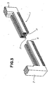
- Figs. 1-5 show an electrical contact assembly having an array of terminal structures according to the present invention.
- the electrical connector 1 comprises an elongated body 4 having extensions 2 and 3 integrally connected to the opposite ends of the elongated body 4.
- a plurality of terminals 11 according to the present invention are fixed to the elongated body 4 at regular intervals.
- each terminal 11 is integrally jointed to a counter terminal 11, and is fixed to the elongated body 4 to face the counter terminal 11.
- each terminal 11 comprises an inverted "T"-shaped soldering connecting portion 12, a trunk 13 integrally connected to the soldering connecting portion 12 and having an extended arm 16 to be inserted in a selected slot 15 of the elongated body 4 and a contact piece 14 integrally connected to the trunk 13.
- the terminal pair is a metal piece which is stamped out from a metal sheet.
- the inverted "T"-shaped soldering connecting portion 12 comprises a relatively large foot 17 and a leg 18 integrally connected to the foot 17 as indicated at 19 and rising from the foot 17.
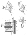
- the foot 17 of each terminal 11 When in use, the foot 17 of each terminal 11 is soldered to a conductor on a printed circuit board 6 to joint the surface of the foot 17 to the surface of the conductor, as indicated at 21.
- the soldering metal is melted and is allowed to invade somewhat the gap remaining between the end surface 20 of the foot 17 and the conductor surface.
- each terminal 11 When another circuit board 8 is inserted between the opposite extensions 2 and 3 of the elongated body 4, the contact 14 of each terminal 11 will be resiliently put in contact with a selected conductor on the printed circuit board 8. Likewise, the contact 14 of the counter terminal 11 will be sandwiched between these contacts 14.
- the foot 17 has a relatively large area. Assume that an undesired exterior force is applied to the contact 14 of the terminal 11 and that the force is transmitted to the soldering skirt 21 via the leg 18, thereby loading the soldering skirt 21. The load per soldering unit area of the foot will not be great because of the increased soldering area which surrounds the relatively large foot 17.
- the terminal 11 is a metal piece stamped out from a metal sheet and therefore the foot-and-leg joint has an increased strength, compared with the one in which a separate leg is integrally connected to a separate foot.
- the inverted "T"-shaped soldering portion of a terminal has a leg and a relatively large foot integrally connected to the center of the leg, thereby causing substantial reduction of load per unit soldering area upon application of an undesired force to the terminal, and increasing the resistivity of the soldering against removal from the conductor on a printed circuit board.
- the leg is integrally connected to the center of the foot, and therefore, an undesired external force when applied to the terminal will be transmitted to the foot and the surrounding soldering skirt so that the foot and the surrounding soldering skirt are evenly stressed, not localizing the force to particular points. Thus, the soldering strength will not be lowered, and the electrical connection will be kept in good condition.
- the terminal is a metal piece which is stamped out from a metal sheet. Therefore, the joint between the foot and the leg has an increased strength. This contributes the solidity with which the soldering portion of the terminal is fixed to the conductor on a printed circuit board.
Landscapes
- Engineering & Computer Science (AREA)
- Manufacturing & Machinery (AREA)
- Microelectronics & Electronic Packaging (AREA)
- Multi-Conductor Connections (AREA)
- Coupling Device And Connection With Printed Circuit (AREA)
- Structures For Mounting Electric Components On Printed Circuit Boards (AREA)
- Connecting Device With Holders (AREA)
Applications Claiming Priority (2)
| Application Number | Priority Date | Filing Date | Title |
|---|---|---|---|
| JP160024/88U | 1988-12-09 | ||
| JP1988160024U JPH0424612Y2 (de) | 1988-12-09 | 1988-12-09 |
Publications (3)
| Publication Number | Publication Date |
|---|---|
| EP0373003A2 true EP0373003A2 (de) | 1990-06-13 |
| EP0373003A3 EP0373003A3 (en) | 1990-12-19 |
| EP0373003B1 EP0373003B1 (de) | 1994-09-21 |
Family
ID=15706317
Family Applications (1)
| Application Number | Title | Priority Date | Filing Date |
|---|---|---|---|
| EP89312876A Expired - Lifetime EP0373003B1 (de) | 1988-12-09 | 1989-12-11 | Kontakt für auf der Oberfläche montierbare Komponente mit einem lötbaren Teil |
Country Status (4)
| Country | Link |
|---|---|
| US (1) | US4955820A (de) |
| EP (1) | EP0373003B1 (de) |
| JP (1) | JPH0424612Y2 (de) |
| DE (1) | DE68918415T2 (de) |
Cited By (12)
| Publication number | Priority date | Publication date | Assignee | Title |
|---|---|---|---|---|
| FR2669149A1 (fr) * | 1990-11-12 | 1992-05-15 | Souriau & Cie | Connecteur intermediaire entre carte de circuit imprime et substrat a circuits electroniques actifs. |
| EP0475067A3 (en) * | 1990-09-10 | 1992-09-16 | Molex Incorporated | Electrical connector and terminal thereof |
| EP0510995A3 (en) * | 1991-04-26 | 1993-04-28 | Amp Incorporated | Electrical connector having reliable terminals |
| EP0594762A4 (en) * | 1991-07-16 | 1997-01-02 | Du Pont | Low profile, surface-mounted connector having curved cantilevered spring contacts |
| EP0774808A1 (de) * | 1995-11-16 | 1997-05-21 | Molex Incorporated | Winkelverbinder für zwei Leiterplatten mit Anti-Kapillarwirkungseigenschaften und dazugehöriges Kontaktelement |
| WO1997045900A1 (en) * | 1996-05-31 | 1997-12-04 | The Whitaker Corporation | Rechargeable battery connector |
| WO1998006149A1 (en) * | 1996-08-05 | 1998-02-12 | The Whitaker Corporation | Electrical connector having thin contacts with surface mount edges |
| US6113440A (en) * | 1997-12-22 | 2000-09-05 | The Whitaker Corporation | Arrangement for resilient contacting |
| WO2004070887A1 (de) * | 2003-02-06 | 2004-08-19 | Siemens Aktiengesellschaft | Smt-fähiges bauelement und leiterplatte |
| US7005311B2 (en) | 1993-09-30 | 2006-02-28 | Osram Gmbh | Two-pole SMT miniature housing for semiconductor components and method for the manufacture thereof |
| US7102215B2 (en) | 1997-07-29 | 2006-09-05 | Osram Gmbh | Surface-mountable light-emitting diode structural element |
| WO2014100391A1 (en) * | 2012-12-21 | 2014-06-26 | Continental Automotive Systems, Inc. | Dynamically stable surface mount post header |
Families Citing this family (19)
| Publication number | Priority date | Publication date | Assignee | Title |
|---|---|---|---|---|
| JPH0628791Y2 (ja) * | 1990-03-20 | 1994-08-03 | モレックス インコーポレーテッド | 電気コネクタにおける端子 |
| US5052936A (en) * | 1990-10-26 | 1991-10-01 | Amp Incroporated | High density electrical connector |
| US5188534A (en) * | 1992-03-19 | 1993-02-23 | Molex Incorporated | Surface mount connector with clip engaging contacts |
| JPH065137U (ja) * | 1992-06-19 | 1994-01-21 | モレックス インコーポレーテッド | 表面実装用電気コネクタに於ける端子 |
| US5310357A (en) * | 1993-02-22 | 1994-05-10 | Berg Technology, Inc. | Blade-like terminal having a passive latch |
| JPH06310197A (ja) * | 1993-04-23 | 1994-11-04 | Matsushita Electric Works Ltd | コネクタ |
| US5451174A (en) * | 1993-06-29 | 1995-09-19 | Autosplice Systems, Inc. | Surface mounted pins for printed circuit boards |
| US5409386A (en) * | 1993-08-18 | 1995-04-25 | Molex Incorporated | Surface mount electrical connector and terminal therefor |
| US5471887A (en) * | 1994-02-01 | 1995-12-05 | The Whitaker Corporation | Removable sensor assembly |
| US5496180A (en) * | 1994-04-06 | 1996-03-05 | The Whitaker Corporation | Surface mountable card edge connector |
| TW280041B (en) * | 1995-10-24 | 1996-07-01 | Connector Systems Tech Nv | Electrical connector with stress isolating solder tail |
| JP3028199B2 (ja) * | 1996-03-14 | 2000-04-04 | モレックス インコーポレーテッド | 電気コネクタのターミナル |
| US5931705A (en) * | 1996-09-11 | 1999-08-03 | Thomas & Betts International | Surface mount wire connector |
| US6095827A (en) * | 1996-10-24 | 2000-08-01 | Berg Technology, Inc. | Electrical connector with stress isolating solder tail |
| US20050101190A1 (en) * | 2003-11-12 | 2005-05-12 | Ong Mei L. | Terminal with flexible tail |
| US7484971B2 (en) * | 2005-11-29 | 2009-02-03 | Amphenol Corporation | Electronic component with high density, low cost attachment |
| US7748994B1 (en) * | 2009-05-13 | 2010-07-06 | Cheng Uei Precision Industry Co., Ltd. | Board-to-board connector assembly |
| US10027046B1 (en) * | 2017-05-23 | 2018-07-17 | Te Connectivity Corporation | Receptacle connector with stub-less contacts |
| US11233348B2 (en) * | 2020-04-24 | 2022-01-25 | Intel Corporation | Structural optimization of contact geometry for high performance connector |
Family Cites Families (8)
| Publication number | Priority date | Publication date | Assignee | Title |
|---|---|---|---|---|
| JPS6270431U (de) * | 1985-10-21 | 1987-05-02 | ||
| JPH0436069Y2 (de) * | 1986-08-29 | 1992-08-26 | ||
| JPS6385838U (de) * | 1986-11-26 | 1988-06-04 | ||
| US4826442A (en) * | 1986-12-19 | 1989-05-02 | Amp Incorporated | Solderable connector retention feature |
| WO1988005612A1 (en) * | 1987-01-23 | 1988-07-28 | Amp Incorporated | High density circuit panel socket |
| US4713013A (en) * | 1987-01-30 | 1987-12-15 | Molex Incorporated | Compliant high density edge card connector with contact locating features |
| JPH0346469Y2 (de) * | 1987-02-26 | 1991-10-01 | ||
| US4802860A (en) * | 1987-03-04 | 1989-02-07 | Hirose Electric Co., Ltd. | Surface mount type electrical connector |
-
1988
- 1988-12-09 JP JP1988160024U patent/JPH0424612Y2/ja not_active Expired
-
1989
- 1989-12-07 US US07/447,350 patent/US4955820A/en not_active Expired - Lifetime
- 1989-12-11 DE DE68918415T patent/DE68918415T2/de not_active Expired - Fee Related
- 1989-12-11 EP EP89312876A patent/EP0373003B1/de not_active Expired - Lifetime
Cited By (19)
| Publication number | Priority date | Publication date | Assignee | Title |
|---|---|---|---|---|
| EP0475067A3 (en) * | 1990-09-10 | 1992-09-16 | Molex Incorporated | Electrical connector and terminal thereof |
| FR2669149A1 (fr) * | 1990-11-12 | 1992-05-15 | Souriau & Cie | Connecteur intermediaire entre carte de circuit imprime et substrat a circuits electroniques actifs. |
| US5152694A (en) * | 1990-11-12 | 1992-10-06 | Souriau Et Cie | Intermediate connector between printed-circuit board and substrate having active electronic circuits |
| EP0510995A3 (en) * | 1991-04-26 | 1993-04-28 | Amp Incorporated | Electrical connector having reliable terminals |
| EP0594762A4 (en) * | 1991-07-16 | 1997-01-02 | Du Pont | Low profile, surface-mounted connector having curved cantilevered spring contacts |
| US7102212B2 (en) | 1993-09-30 | 2006-09-05 | Osram Gmbh | Two-pole SMT miniature housing for semiconductor components and method for the manufacture thereof |
| US7005311B2 (en) | 1993-09-30 | 2006-02-28 | Osram Gmbh | Two-pole SMT miniature housing for semiconductor components and method for the manufacture thereof |
| US7288831B2 (en) | 1993-09-30 | 2007-10-30 | Osram Gmbh | Two-pole SMT miniature housing for semiconductor components and method for the manufacture thereof |
| EP0774808A1 (de) * | 1995-11-16 | 1997-05-21 | Molex Incorporated | Winkelverbinder für zwei Leiterplatten mit Anti-Kapillarwirkungseigenschaften und dazugehöriges Kontaktelement |
| WO1997045900A1 (en) * | 1996-05-31 | 1997-12-04 | The Whitaker Corporation | Rechargeable battery connector |
| US5823801A (en) * | 1996-08-05 | 1998-10-20 | The Whitaker Corporation | Electrical connector having thin contacts with surface mount edges |
| WO1998006149A1 (en) * | 1996-08-05 | 1998-02-12 | The Whitaker Corporation | Electrical connector having thin contacts with surface mount edges |
| US7102215B2 (en) | 1997-07-29 | 2006-09-05 | Osram Gmbh | Surface-mountable light-emitting diode structural element |
| US7183632B2 (en) | 1997-07-29 | 2007-02-27 | Osram Gmbh | Surface-mountable light-emitting diode structural element |
| US7508002B2 (en) | 1997-07-29 | 2009-03-24 | Osram Gmbh | Surface-mountable light-emitting diode structural element |
| US6113440A (en) * | 1997-12-22 | 2000-09-05 | The Whitaker Corporation | Arrangement for resilient contacting |
| WO2004070887A1 (de) * | 2003-02-06 | 2004-08-19 | Siemens Aktiengesellschaft | Smt-fähiges bauelement und leiterplatte |
| WO2014100391A1 (en) * | 2012-12-21 | 2014-06-26 | Continental Automotive Systems, Inc. | Dynamically stable surface mount post header |
| US9276337B2 (en) | 2012-12-21 | 2016-03-01 | Continental Automotive Systems, Inc. | Dynamically stable surface mount post header |
Also Published As
| Publication number | Publication date |
|---|---|
| EP0373003B1 (de) | 1994-09-21 |
| JPH0280970U (de) | 1990-06-21 |
| JPH0424612Y2 (de) | 1992-06-10 |
| EP0373003A3 (en) | 1990-12-19 |
| US4955820A (en) | 1990-09-11 |
| DE68918415T2 (de) | 1995-03-16 |
| DE68918415D1 (de) | 1994-10-27 |
Similar Documents
| Publication | Publication Date | Title |
|---|---|---|
| EP0373003B1 (de) | Kontakt für auf der Oberfläche montierbare Komponente mit einem lötbaren Teil | |
| KR970000291Y1 (ko) | 표면 장착 전기 커넥터 어셈블리 | |
| US4621880A (en) | Electrical contact elements, connectors and assemblies | |
| US4009921A (en) | Electrical contact and support means therefor | |
| US4353609A (en) | Terminal for printed circuit boards | |
| EP0475067B1 (de) | Elektrischer Steckverbinder und Endstück dafür | |
| US7430801B2 (en) | Connector assembly | |
| EP0564955A2 (de) | Randverbinder für eine Leiterplatte | |
| EP1058352B1 (de) | Elektrischer Verbinder | |
| JPH0754720B2 (ja) | フレキシブルプリント回路板用電気接続端子 | |
| JPH0631088U (ja) | エッジコネクタ及びそれに使用する接触子 | |
| KR920007828B1 (ko) | 인쇄 회로 기판상에 ic 칩 패키지를 장착시키기 위한 소켓 | |
| JPS6229084A (ja) | 接点装置とその製造法 | |
| JP3148855B2 (ja) | 電気コネクタ | |
| US4638406A (en) | Discrete component mounting assembly | |
| KR980007880A (ko) | 전기 도체 | |
| EP0724782B1 (de) | Mehrfachmodularstecker | |
| US5141450A (en) | Tape carrier type electrical connector | |
| US4681391A (en) | Electric connector | |
| US3264596A (en) | Printed circuit board connector | |
| US4922380A (en) | Junction box containing a printed circuit board | |
| JPH0348635B2 (de) | ||
| JPH09155U (ja) | エッジコネクタ | |
| KR960001307Y1 (ko) | 암 전기 접촉 장치 | |
| JPH0548383Y2 (de) |
Legal Events
| Date | Code | Title | Description |
|---|---|---|---|
| PUAI | Public reference made under article 153(3) epc to a published international application that has entered the european phase |
Free format text: ORIGINAL CODE: 0009012 |
|
| AK | Designated contracting states |
Kind code of ref document: A2 Designated state(s): DE FR GB |
|
| PUAL | Search report despatched |
Free format text: ORIGINAL CODE: 0009013 |
|
| AK | Designated contracting states |
Kind code of ref document: A3 Designated state(s): DE FR GB |
|
| 17P | Request for examination filed |
Effective date: 19910528 |
|
| 17Q | First examination report despatched |
Effective date: 19930524 |
|
| GRAA | (expected) grant |
Free format text: ORIGINAL CODE: 0009210 |
|
| AK | Designated contracting states |
Kind code of ref document: B1 Designated state(s): DE FR GB |
|
| REF | Corresponds to: |
Ref document number: 68918415 Country of ref document: DE Date of ref document: 19941027 |
|
| ET | Fr: translation filed | ||
| PLBE | No opposition filed within time limit |
Free format text: ORIGINAL CODE: 0009261 |
|
| STAA | Information on the status of an ep patent application or granted ep patent |
Free format text: STATUS: NO OPPOSITION FILED WITHIN TIME LIMIT |
|
| 26N | No opposition filed | ||
| REG | Reference to a national code |
Ref country code: GB Ref legal event code: IF02 |
|
| PGFP | Annual fee paid to national office [announced via postgrant information from national office to epo] |
Ref country code: GB Payment date: 20021104 Year of fee payment: 14 |
|
| PGFP | Annual fee paid to national office [announced via postgrant information from national office to epo] |
Ref country code: DE Payment date: 20021230 Year of fee payment: 14 |
|
| PGFP | Annual fee paid to national office [announced via postgrant information from national office to epo] |
Ref country code: FR Payment date: 20031201 Year of fee payment: 15 |
|
| PG25 | Lapsed in a contracting state [announced via postgrant information from national office to epo] |
Ref country code: GB Free format text: LAPSE BECAUSE OF NON-PAYMENT OF DUE FEES Effective date: 20031211 |
|
| PG25 | Lapsed in a contracting state [announced via postgrant information from national office to epo] |
Ref country code: DE Free format text: LAPSE BECAUSE OF NON-PAYMENT OF DUE FEES Effective date: 20040701 |
|
| GBPC | Gb: european patent ceased through non-payment of renewal fee |
Effective date: 20031211 |
|
| PG25 | Lapsed in a contracting state [announced via postgrant information from national office to epo] |
Ref country code: FR Free format text: LAPSE BECAUSE OF NON-PAYMENT OF DUE FEES Effective date: 20050831 |
|
| REG | Reference to a national code |
Ref country code: FR Ref legal event code: ST |