EP0367195A2 - Mim cold-cathode electron emission elements and methods of manufacture thereof - Google Patents
Mim cold-cathode electron emission elements and methods of manufacture thereof Download PDFInfo
- Publication number
- EP0367195A2 EP0367195A2 EP89120124A EP89120124A EP0367195A2 EP 0367195 A2 EP0367195 A2 EP 0367195A2 EP 89120124 A EP89120124 A EP 89120124A EP 89120124 A EP89120124 A EP 89120124A EP 0367195 A2 EP0367195 A2 EP 0367195A2
- Authority
- EP
- European Patent Office
- Prior art keywords
- electron emission
- layer
- insulating layer
- metal layer
- portions
- Prior art date
- Legal status (The legal status is an assumption and is not a legal conclusion. Google has not performed a legal analysis and makes no representation as to the accuracy of the status listed.)
- Withdrawn
Links
Images


Classifications
-
- H—ELECTRICITY
- H01—ELECTRIC ELEMENTS
- H01J—ELECTRIC DISCHARGE TUBES OR DISCHARGE LAMPS
- H01J9/00—Apparatus or processes specially adapted for the manufacture, installation, removal, maintenance of electric discharge tubes, discharge lamps, or parts thereof; Recovery of material from discharge tubes or lamps
- H01J9/02—Manufacture of electrodes or electrode systems
- H01J9/022—Manufacture of electrodes or electrode systems of cold cathodes
-
- B—PERFORMING OPERATIONS; TRANSPORTING
- B82—NANOTECHNOLOGY
- B82Y—SPECIFIC USES OR APPLICATIONS OF NANOSTRUCTURES; MEASUREMENT OR ANALYSIS OF NANOSTRUCTURES; MANUFACTURE OR TREATMENT OF NANOSTRUCTURES
- B82Y10/00—Nanotechnology for information processing, storage or transmission, e.g. quantum computing or single electron logic
-
- H—ELECTRICITY
- H01—ELECTRIC ELEMENTS
- H01J—ELECTRIC DISCHARGE TUBES OR DISCHARGE LAMPS
- H01J1/00—Details of electrodes, of magnetic control means, of screens, or of the mounting or spacing thereof, common to two or more basic types of discharge tubes or lamps
- H01J1/02—Main electrodes
- H01J1/30—Cold cathodes, e.g. field-emissive cathode
- H01J1/312—Cold cathodes, e.g. field-emissive cathode having an electric field perpendicular to the surface, e.g. tunnel-effect cathodes of Metal-Insulator-Metal [MIM] type
Landscapes
- Engineering & Computer Science (AREA)
- Chemical & Material Sciences (AREA)
- Nanotechnology (AREA)
- Manufacturing & Machinery (AREA)
- Physics & Mathematics (AREA)
- Mathematical Physics (AREA)
- Theoretical Computer Science (AREA)
- Crystallography & Structural Chemistry (AREA)
- Cold Cathode And The Manufacture (AREA)
Abstract
Description
- The present invention relates to structures and methods of manufacture for an electron emission element which can be utilized as a source of electron emission, for use in various types of apparatus which utilize an electron beam, such as electron microscopes, CRTs, etc. In particular, the invention is directed towards improved structures and methods of manufacture for thin-film electron emission elements which are basically of a metal - insulation - metal layer configuration.
- In the prior art, a heated cathode is used for electron emission in equipment which uses an electron beam, such as electron microscopes and CRTs. However, with a heated cathode it is of course necessary to provide heating means to produce electron emission, and this has the disadvantage of high energy consumption. For this reason, various types of electron emission elements have been researched which provide electron emission without heating, i.e. cold-cathode electron emission elements.
- As a specific example, if a reverse bias voltage is applied to a PN junction, then an avalanche condition can be produced whereby electron emission from the PN junction can be obtained. Alternatively, a localized high-intensity electric field can be applied to a metal electrode, causing field-effect electron emission to occur. Another method is to use a device having a metal - insulator - metal layer configuration (i.e. an MIM type of electron emission element), where the insulating layer and one of the metal layers are respectively formed as extremely thin films, and with the thin metal layer being disposed in a vacuum, and to apply a voltage between the two metal layers whereby electrons execute tunnelling through the insulating layer and a proportion of these are then emitted from the thin metal layer. Of the above types of cold-cathode devices, the MIM electron emission element has the advantage of a simple type of construction, and will be described in the following.
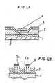
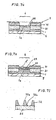
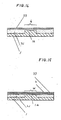
- The basic principles of an MIM electron emission element are illustrated in Fig. 1. A metal layer (conducting material layer) 41 has a very thin insulating layer 42 formed thereon, and a very
thin metal layer 43 is formed upon the insulating layer 42. The upper surface of themetal layer 43 is exposed to a vacuum, or low pressure gas. By applying a voltage from apower source 44 between themetal layers 41 and 43, having a value that is greater than the work function of themetal layer 43, electron tunnelling through the insulating layer 42 will occur. Some of the tunnelling electrons will have a greater energy than the vacuum potential, and so are emitted from the surface of themetal layer 43, as emittedelectrons 45. - Figs. 2 and 3 show respective specific examples of a prior art type of MIM electron emission element. With the electron emission element of Fig. 2, a metal layer 52 consisting of Al and a
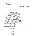
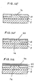
metal layer 55 consisting of Au are successively formed on a surface of aglass substrate 51. An insulating layer 52, consisting of Al₂O₃ and an electrically insulatinglayer 54 consisting of SiO₂ are formed between themetal layers 52 and 55. When a voltage is applied between themetal layers 52 and 55, electrons are emitted from theelectron emission region 56 of themetal layer 55. This is described in the Electronic Apparatus Reasearch Conference Papers of the Television Society, with the title "Cathode Ray Tube Using Tunnel Cathode", 1968, 4, 30. - With the prior art MIM electron emission element of Fig. 3, the
metal layer 62 is formed as a strip upon the surface of an electrically insulatinglayer 61, then an electrically insulatinglayer 63 is formed on themetal layer 62. Next, ametal layer 64 is formed upon theinsulating layer 63, also in the shape of a strip, positioned such as to perpendicularly intersect themetal layer 62. When a voltage is applied between themetal layers metal layer 64, with the area of this electron emission region being defined as the region of intersection between the two metal layers. This electron emission element is described in Japanese Patent Laid-open No. 63-6717. - However with the above types of prior art MIM electron emission element, the problem arises that the electron emission distribution within the electron emission region is non-uniform, i.e. there are positions within the electron emission region at which the rate of electron emission is high, and regions where emission is low. Furthermore, with such a prior art type of electron emission element, in addition to the problem of unevenness of electron emission, the metal layer that is formed on the insulating layer will in many cases have poor electrical conductivity.
- The reason for the non-uniformity of electron emission distribution is as follows. In order to maximize the efficiency of electron emission from the metal layer that is formed on the insulating layer, that metal layer must be made extremely thin within the electron emission region. However since it is difficult to form the electron emission region with a very uniform thickness of thin metal film, there will inevitably be some variations in thickness within the electron emission region. This results in non-uniformity of electron emission distribution in the electron emission region. Furthermore, due to the fact that the metal layer is very thin, successive voltage drops will occur within that layer, from the point of connection of the metal layer to a power source. Thus, the effective electric field strength within the electron emission region will be non-uniform, causing the electron emission to be uneven within that region. In addition, those electrons which are unable to leave the metal layer by being emitted therefrom, after having passed through the insulating layer by tunnelling, will produce a flow of current within the metal layer. The greater the level of this current flow, i.e. the lower the efficiency of electron emission of the element, the greater will be an amount of Joule heating that is produced in the thin metal layer, whereby heat is generated within portions of that layer. As a result, it becomes impossible to apply a stable and uniform electric field to the insulating layer within the electron emission region, whereby uniformity of electron emission is prevented.
- The reasons for the poor conduction of the metal layer are as follows. With the electron emission element of Fig. 3, there are step variations in the height of the surface of the insulating layer, and corresponding step changes are produced in the metal layer that is formed on the insulating layer. Due to these step changes in shape of the layers, corners are formed, and as a result of these corners formed in the layers, defects are produced in the thin metal layer, so that poor electrical conduction in that layer will occur.
- Another problem which arises with such a prior art type of MIM electron emission element is that the electron emission efficiency is insufficient. The insulating layer is formed in the prior art as a very thin film, having a thickness of approximately 50 to 200 Å, by a process such as evaporative deposition, anodic oxidation, etc.and is not formed with a crystal structure, i.e. is an amorphous layer. As a result, most of the electrons which move within the insulating layer by the tunnelling effect will be dispersed within that layer as a result of collisions with atoms of the material constituting the layer, and will thereby lose energy, so that the number of electrons which actually are transferred to the thin metal layer of such an electron emission element will be very small.
- In addition, the electrons which enter this thin metal layer will also be dispersed, and suffer a further energy loss thereby. In order to reduce this dispersion within the thin metal layer, that layer must be made as thin as possible, However if that layer is made very thin, then a substantial voltage drop will occur between the point of connection of that metal layer to a power source terminal and an electron emission region of the metal layer, as described above. Thus, the intensity of the electric field that is produced in a region of the insulating layer immediately below an electron emission region of the thin metal layer is reduced, and hence effective electron emission cannot be achieved. This reduction of effective electric field strength within the electron emission region can be counteracted to some extent by increasing the level of voltage supplied by the power source. However in that case, Joule heating will occur due to the electrical power which will be dissipated within the metal layer, resulting in non-uniform electron emission and the danger of open-circuits in the thin metal layer.
- Furthermore, with such an MIM type of electron emission element, both the thin-film insulating layer (through which the tunnelling electrons pass) and the thin-film metal layer (from which electrons are emitted) are formed upon an underlying layer which has an upwardly protruding portion and/or an inwardly recessed portion, i.e. which has an upper surface that exhibits step changes in height. As a result, each of the thin insulating layer and thin metal layer will also have corresponding step changes in height, so that the respective film thicknesses of these layers will be non-uniform. Hence, the operating characteristics of such an electron emission element are unstable. In particular, if the thin metal layer is formed with such step variations in height, then internal defects may be produced within that layer in regions which are close to these step changes, i.e. at corner portions. This can result in localized variations in electrical conduction at these portions, as well as non-uniformity of film thickness, thereby further contributing to deterioration of the electrical characteristics. Moreover, if an array is formed of a plurality of such MIM electron emission elements, the characteristics of respective elements of the array will vary significantly from one another.
- It is a first objective of the present invention to provide an MIM type of electron emission element which overcomes the above problem of non-uniform of electron emission distribution of prior art devices.
- It is a second objective of the present invention to provide an MIM type of electron emission element which has high reliability of electrical conduction of a metal layer from which electrons are emitted.
- It is a third objective of the present invention to provide an MIM type of electron emission element whereby dispersion of electrons which travel through a thin insulating layer by the tunnelling effect is suppressed, to thereby achieve an enhanced degree of electron emission efficiency.
- It is a fourth objective of the present invention to provide an MIM type of electron emission element whereby even when a region of a metal layer from which electrons are emitted is made extremely thin, voltage drops within that metal layer and open-circuits resulting from power dissipation within that layer are effectively prevented.
- It is a fifth objective of the present invention to provide an MIM type of electron emission element whereby each of a thin insulating layer through which electrons pass by the tunnelling effect and a thin metal layer from which electrons are emitted is formed as a completely flat layer.
- It is a sixth objective of the present invention to provide a simple method of manufacture for an MIM type of electron emission element whereby prior art problems of non-uniform electron emission distribution are overcome.
- According to one aspect, an electron emission element according to the present invention comprises an electrically insulating material formed on a layer of electrically conducting material (or a bulk conducting body), with a metal layer formed over the insulating layer. Immediately below an electron emission region of the metal layer, the insulating layer is formed as an extremely thin film, while the metal layer within the electron emission region is formed as an array of thick and thin portions which are distributed throughout that region. The thick portions of the metal layer serve to ensure that a sufficient level of voltage will be applied to the thin portions, while the thin portions are made sufficiently thin to ensure high efficiency of electron emission.
- It has been found that such an array of thick and thin portions of the metal layer can be very easily formed by executing evaporative deposition of a metal through a mask having a pattern of apertures therein, if the mask is positioned spaced apart from the insulating layer by a specific distance. The "thin portions" in this case are constituted by sloping edge portions which extend from each thick portion.
- The thin insulating layer portion corresponding to the electron emission region can be formed by providing an upwardly protruding portion of the conducting layer, and forming an insulating layer which covers the upwardly protruding portion and surrounding regions of the conducting layer and has a flat upper surface. Alternatively, a first insulating layer can be formed surrounding the upwardly protruding portion of the conducting layer, to the same height as that upwardly protruding portion, and a thin insulating layer then formed overall, with a flat upper surface. It is also possible to form the latter thin insulating layer as an oxide film on the upwardly protruding portion of the conducting layer. In each case, an overall insulating layer having a flat upper surface is formed, on which the thin metal layer is then deposited as a completely flat thin film. With such a configuration, the shape of the electron emission region of the electron emission element can be selected as required, by the shape of the upwardly protruding portion of the conducting layer.
- According to another aspect of the invention, the thin insulating layer below the electron emission region is formed as an epitaxially grown layer of single-crystal material, with the crystal planes oriented with respect to the layer surface such as to minimize dispersion of electrons which pass through that insulating layer by tunnelling. The efficiency of electron emission can thereby be substantially increased.
- More specifically, one embodiment of the invention is an electron emission element comprising an electrically conducting layer, an electrically insulating layer formed on the conducting layer, and a metal layer formed on the insulating layer, wherein the metal layer is formed with an electron emission region comprising a plurality of relatively thick portions of the metal layer and a plurality of relatively thin portions of the metal layer, the thick and thin portions being distributed throughout the electron emission region.
- Another embodiment of the invention is an electron emission element comprising an electrically conducting body having an electrically insulating layer formed thereon, and a metal layer formed on the insulating layer, with respective values of thickness of at least portions of the insulating layer and metal layer being selected such as to permit electron emission from an electron emission region of the metal layer in response to application of a specific level of voltage between the conducting body and the metal layer, wherein at least a part of the insulating layer corresponding in position to the electron emission region comprises a single-crystal layer of an electrically insulating material having crystal planes thereof oriented in predetermined directions.
- Another emodiment of the invention is an electron emission element comprising a substrate, an electrically conducting layer formed on a predetermined region of a surface of the substrate, a first electrically insulating layer formed on the conducting layer, a second insulating layer formed on a region of the substrate outside the first insulating layer, with an upper surface of the second insulating layer being co-planar with an upper surface of the first insulating layer, and a metal layer formed on the first and second insulating layers.
- Yet another embodiment of the invention is an electron emission element comprising an electrically conducting body having a surface thereof formed with an upwardly protruding portion, an electrically insulating layer formed to cover the conducting body and having a flat upper surface, and a metal layer formed upon the insulating layer surface, the metal layer extending above the upwardly protruding portion of the conducting body and at least partially overlapping a boundary of the upwardly protruding portion.
- A further embodiment of the invention is an electron emission element comprising an electrically conducting body formed on a portion of a surface of a substrate, an electrically insulating layer formed upon the conducting body and the surface, the insulating layer having a flat upper surface, and a metal layer formed on the insulating layer surface, extending above the conducting body.
- The invention further describes a method of manufacture for an electron emission element, comprising successive steps of:
forming a layer of an electrically conducting material on a surface of a glass substrate;
forming a layer of an electrically insulating material on the conducting material layer;
forming a metal layer upon the layer of insulating material;
forming a patterned photoresist layer on the metal layer; and
executing photo-lithography etching of the metal layer, employing the photoresist layer, to selectively remove portions of the metal layer. - The invention moreover includes aa method of manufacture for an electron emission element, comprising successive steps of:
forming a layer of an electrically insulating material on a region of a conducting body corresponding to an electron emission region, the thickness of the layer of insulating material being selected such as to permit an electron tunnelling effect to occur in the layer of insulating material; and
executing evaporative deposition of a metal onto a surface of the insulating layer through a mask, the mask having a predetermined pattern of apertures formed therein, and the mask being spaced apart from the layer of insulating material by a predetermined distance;
for thereby forming a plurality of thick portions and a plurality of sloping portions of the metal layer within the electron emission region, each of the sloping portions being integrally formed with a corresponding one of the thick portions and being of gradually varying thickness, the thick portions and thin portions being distributed throughout the electron emission region. -
- Fig. 1 is a conceptual cross-sectional view for describing the basic principles of a MIM electron emission element;
- Fig. 2 is a general cross-sectional view of an example of a prior art MIM type of electron emission element;
- Fig. 3 is a general oblique view of another example of a prior art MIM type of electron emission element;
- Fig. 4A is a general cross-sectional view of a first embodiment of an electron emission element according to the present invention;
- Fig. 4B is an expanded cross-sectional view of an electron emission region in the embodiment of Fig. 4A;
- Figs. 5A to 5C are diagrams showing a second embodiment of an MIM type of electron emission element according to the present invention, in which Fig. 5A is a cross-sectional view, Fig. 5B is an expanded partial cross-sectional view of a metal layer in Fig. 5A, and Fig 5C is a partial expanded plan view of a metal layer in Fig. 5A;
- Figs. 6A and 6B show a third embodiment of an electron emission element according to the present invention, in which Fig. 6A is a cross-sectional view and Fig. 6B is a partial expanded cross-sectional view of a metal layer;
- Figs. 7A to 7I are diagrams illustrating steps of a method of manufacture for the electron emission element of Figs. 6A to 6B;
- Fig. 8 is a general cross-sectional view of a fourth embodiment of an electron emission element according to the present invention;
- Fig. 9 is a general cross-sectional view of a fifth embodiment of an electron emission element according to the present invention;
- Fig. 10A is a plan view of a sixth embodiment of an electron emission element according to the present invention, and Fig.. 10B is a corresponding cross-sectional view;
- Fig. 11 is a general cross-sectional view of a seventh embodiment of an electron emission element according to the present invention;
- Figs. 12A to l2G are cross-sectional views illustrating steps of a method of manufacture for the electron emission element of Fig. 11
- Fig. 13 is a general cross-sectional view of an eighth embodiment of an electron emission element according to the present invention;
- Fig. 14 is a general cross-sectional view of a ninth embodiment of an electron emission element according to the present invention;
- Fig. 15 is a general cross-sectional view of a tenth embodiment of an electron emission element according to the present invention;
- Figs. 16A to 16G are cross-sectional views illustrating steps of a method of manufacture for the electron emission element of Fig.15; and
- Figs. 17 and 18 are general cross-sectional views showing an eleventh and a twelfth embodiment of an electron emission element according to the present invention, respectively.
- Embodiments of the invention will be described in the following, referring to the drawings.
- It should be noted that terms such as "upper", "upward", "upwardly protruding" etc. as applied to layers formed in the various embodiments, which assume that each embodiment is oriented as indicated in the respective drawings, with an electron emission metal layer oriented horizontally as an uppermost layer, are of course used only for simplicity of description,
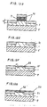
- Fig. 4A is a general cross-sectional view of a first embodiment of an electron emission element according to the present invention. Fig. 4B is an expanded view of a portion of an electron emission region that is located within a broken-line outline shown in Fig 4A. In these figures, numeral 1 denotes a layer of an electrically conducting material which is formed on a
substrate 5,numeral 2 denotes an insulating layer which is formed on theconducting layer 1,numeral 3 denotes a metal layer formed on the insulatinglayer 2,numeral 4 denotes an electron emission region at the center of themetal layer 3,numeral 5 denotes a substrate which is the lowest layer, and numeral 6 denotes electrons which are emitted from theelectron emission region 4. - An example of a method of manufacture for such an electron emission element is as follows. On a
glass substrate 5 is formed a thin film of Al as theconducting layer 1, to a thickness of 3,000 to 5,000 Å approximately, by a method such as vacuum evaporative deposition or by sputtering deposition. A layer of a material such as Al₂O₃ or SiO₂ is then formed on a region of theAl film 1 which corresponds to theelectron emission region 4, as the insulatinglayer 2, by a method such as vacuum evaporative deposition or sputtering deposition, or by anodic oxidation, to a thickness of 50 Å to 200 Å. Thiselectron emission region 4 has a diameter of approximately 100µm. Next, a layer of a metal such as Au or Al is formed as themetal layer 3, upon the insulatinglayer 2. As shown in Fig. 4B, themetal layer 3 consists ofthin portions 3b (each having a film thickness of 50 Å to 200 Å approximately) and thick portions 3a (each having a film thickness of 1000 Å approximately). Thismetal layer 3 is formed by a method such as vacuum evaporative deposition or by sputtering deposition. - An example of a method of forming the thick and
thin portions 3a and 3b of themetal layer 3 is as follows A layer of Au or Al is formed on the insulatinglayer 2, by a process such as vacuum evaporative deposition or sputtering deposition, to a thickness of approximately 1000 Å, then a layer of photoresist is formed thereon, and the photoresist is then exposed to a pattern of light which has a pitch of approximately 10µm. The photoresist is then developed and the portions of photoresist corresponding to the regions within theelectron emission region 4 that are to be made thin are removed. Etching of these regions of themetal layer 3, to a depth which is close to the surface of the insulatinglayer 2, is then performed. The remaining photoresist is then removed. - It can be understood that with such an element, each of the thin portions of the metal layer within the electron emission region is integrally connected to at least one corresponding thick portion. Thus, by applying a voltage between the conducting
layer 1 and themetal layer 3 of such an MIM electron emission element, such that themetal layer 3 is made positive, a voltage is applied through the thick portions 3a of themetal layer 3 to thethin portions 3b. Since the voltage drop which occurs in the thick portions 3a is very small, substantially uniform values of voltage are applied to thethin portions 3b, whereby uniform emission of electrons 6 is obtained from the thin portions 3a in the electron emission region. - Figs. 5A to 5C illustrate a second embodiment of an electron emission element according to the present invention. With this embodiment, an electrically conducting layer 1 (consisting of a material such as Al) is formed on an electrically insulating substrate 5 (consisting of a material such as glass) . An electrically insulating layer 2 (consisting of a material such as Al₂O₃ of SiO₂) is formed as a thin film on the
conducting layer 1. A thin metal film 3 (e.g. consisting of Au) is formed on the insulatinglayer 2. The thickness of theconducting layer 1 is approximately 1000 to 5000 Å. The thickness of the insulatinglayer 2 is approximately 50 to 200 Å, within anelectron emission region 4, and is 2000 to 5000 Å in areas outside theelectron emission region 4. The thickness of thethin metal film 3 is 500 to 2000 Å in areas outside theelectron emission region 4. - The configuration of the
electron emission region 4 of thethin metal film 3 is as follows. As shown in Fig 5C, theelectron emission region 4 is formed with a plurality of mutually parallel narrow stripe-shapedportions 3′, with regions of the surface of the insulatinglayer 2 between thesestripe portions 3′ being left exposed (i.e without metal having been deposited thereon). As shown in Fig. 5B, which is an expanded cross-sectional view of the portion A of Fig. 5A, each of theseportions 3′ of thethin metal film 3 has a flat-toppedportion 3′a andsloping portions 3′b. Each of these slopingportions 3′b gradually decreases in thickness from a maximum value to a value of zero, i.e to finally reach the surface of the insulatinglayer 2. The central region of each flat-topped portion is a thick portion of the metal layer, which serves to ensure low electrical resistance, while regions which are centered on the slopingportions 3′b of the metal layer constitute thin portions which serve for electron emission. As shown, a large number of thesestripe portions 3′ having slopingportions 3′b and flat-toppedportions 3′a are widely distributed throughout theelectron emission region 4. Thus, the thin electron emission portions are widely distributed throughout theelectron emission region 4, with each thin portion being of course integrally connected to a thick portion of the metal layer. The thickness of each of the flat-toppedportions 3′a of thethin metal film 3 is approximately 500 to 2000 Å. - When a voltage is applied between the conducting
layer 1 and thethin metal film 3, then due to the low electrical resistance that is ensured by the flat-toppedportions 3′a, voltage drops are prevented. This ensures that a strong electric field is produced, so that electrons are strongly emitted from the overall area of theelectron emission region 4. - In the embodiment described above, as shown in Figs. 5B and 5C, mutually adjacent ones of the sloping portions are separated from one another, with an exposed region of the surface of the insulating
layer 2 being formed therebetween. However it would be equally possible to modify that embodiment such that mutually adjacent ones of the sloping portions are connected to one another, i.e. are mutually connected by a region of minimum thickness, so that no exposed regions of the insulatinglayer 2 are formed between them. It has been found that if this is done, then the results obtained are similar to those obtained for an electron emission element of the form shown in Figs. 4A, 4B. - A third embodiment of an electron emission element according to the present invention is as follows. With this electron emission element, as shown in Fig. 6A, an electrically conducting layer 1 (consisting of a material such as Al) is formed on an electrically insulating substrate 5 (consisting of a material such as glass). An insulating layer 2 (consisting of a material such as Al₂O₃ of SiO₂) is formed on the
conducting layer 1. A metal layer 3 (consisting of a material such as Au) is formed on the insulatinglayer 2. - The configuration of the
electron emission region 4 of themetal layer 3 is similar to that of the preceding embodiment. As shown in the expanded cross-sectional view of Fig. 6B showing the portion A′ in Fig. 6A, theelectron emission region 4 has a plurality of parallel narrow stripe-shapedportions 3′, with regions of the surface of the insulatinglayer 2 between thesestripe portions 3′ being left exposed. As shown, each of theseportions 3′ of themetal layer 3 has a flat-toppedportion 3′a andsloping portions 3′b which gradually decrease in thickness to finally reach the surface of the insulatinglayer 2. - With this embodiment, the surface of the
conducting layer 1 has an upwardly protruding portion 1a corresponding to the position of theelectron emission region 4, and the thickness of the portion of the insulatinglayer 2 that is immediately above this upwardly protruding portion 1a is accordingly decreased. Thus, the boundary of theelectron emission region 4 is defined by the shape of the upper surface of this upwardly protruding portion 1a. - The surface of the insulating
layer 2 is flat, so that themetal layer 3 is formed over this entire surface without any step changes in height of thelayer 3, i.e. the interface between the insulatinglayer 2 and themetal layer 3 is a single plane, which extends inside and outside theelectron emission region 4. Hence, a high degree of reliability of electrical conduction is achieved for themetal layer 3, since that layer can be formed as a single uniform flat film, without corners being formed therein, and hence with a low possibility of defects being formed therein. In addition, themetal layer 3 is thinner within theelectron emission region 4 than it is outside theregion 4, so that it is easy to ensure that both a high efficiency of electron emission and low electrical resistance are attained. - Furthermore with such an electron emission element, when a voltage is applied between the
metal layer 3 and theconducting layer 1, then due to the low electrical resistance that is ensured by the flat-toppedportions 3′a, voltage drops are prevented, and a strong electric field is produced, so that electrons are strongly emitted over the entire area of theelectron emission region 4. - An example of a method of manufacture for the embodiment of Figs. 6A and 6B will be described in the following, referring to Figs. 7A to 7I.
- Firstly, a metal layer (consisting of a material such as Al or Ta) is formed on the surface of an insulating
substrate 5, consisting of a material such as glass. The metal layer can be formed by by a process such as resistive evaporative deposition, electron beam evaporative deposition, or sputtering deposition deposition; and is formed to a thickness of approximately 1000 to 10,000 Å. In this way anelectrically conducting layer 1 is deposited as shown in Fig 7A. After thus forming thelayer 1, then as shown in Fig. 7B a layer ofphotoresist 7 is selectively formed at positions where theelectron emission region 4 is to be formed. Thephotoresist layer 7 can be formed by the usual photolithography technique. - After forming the
photoresist layer 7, ion milling or liquid etching is executed to etch those regions of theconducting layer 1 that are not covered with the photoresist, with etching being performed to a depth d of for example 500 to 5,000 Å. The upwardly protruding portion 1a is thereby formed. Next, as shown in Fig. 7D, the insulating layer 21 (consisting of a material such as SiO₂, Al₂O₃, or Ta₂O₅) is formed overall, to the same height as that of the upwardly protruding portion 1a (i.e. to a thickness which is equal to the etching depth d), by a process such as resistive evaporative deposition, electron beam evaporative deposition, or sputtering deposition. - After depositing the insulating
layer 21, as shown in Fig. 7E, themetal layer 31 is formed to a thickness of approximately 200 to 1,000 Å (consisting of a material such as Au, Al, Mo or W) , by a process such as resistive heating evaporative deposition, electron beam evaporative deposition, or sputtering deposition. - Next, after removing the
photoresist layer 7, oxidation of the surface of the upwardly protruding portion 1a is performed, to a thickness of approximately 50 to 200 Å, whereby as shown in Fig. 7F the thin insulating layer (i.e. oxide insulation film) 22 is formed This is done by a process such as thermal oxidation in an oxygen atmosphere, or anodic oxidation, to form a layer of a material such as Al₂O₃, Ta₂O₅, etc. When this is completed, an electrically insulating layer has been formed from the insulatinglayers - Next, the metal layer of the
electron emission region 4 is formed. As shown in Fig. 7G, amask 8 is positioned with a fixed small amount of separation from the surface of the insulatinglayer 22, then a metal layer (consisting of a material such as Au, Al, Mo, W, etc) is deposited by evaporative deposition through themask 8, to a thickness of 100 to 500 Å approximately, by a process such as resistive heating evaporative deposition, electron beam evaporative deposition or sputtering deposition. Themask 8 is provided with open slits at specific positions which correspond to positions where the metal layer is to be formed. These can be for example a parallel array of slits, each having a width of 0.01 to 0.05 mm, a length of 0.5 mm to 1 mm, and a pitch of 0.05 to 0.1 mm. - In this way, as a result of deposition of the metal layer as shown in Fig. 7H, a
metal layer 32 is formed in theelectron emission region 4. Fig. 7I is an expanded view of the portion A′ of thismetal layer 32. As shown, this consists of flat-toppedportions 32a and sloping portions 32b , which result from themask 8 having been positioned with a slight separation from the surface of the insulatinglayer 22. - With the electron emission element of Fig. 7H, when compared to the configuration shown in Fig. 6A, the insulating
layers layer 2, and the metal layers 31, 32 correspond to themetal layer 3. It can thus be understood that both of these electron emission elements are of basically identical configuration. - It should be noted that it would be equally possible to form the metal layer of the electron emission region by first forming a metal layer to the desired thickness for the flat-topped portions over the entire area of the electron emission region, and to then execute selective removal of that layer to a predetermined thickness, at positions such as to ensure that the thick portions and the thin portions (for electron emission) of the metal layer will be uniformly distributed throughout the electron emission region.
- In the above embodiments, formation of a single electron emission region is described. However it would be equally possible to produce an array of such electron emission elements, i.e. by forming an array of such electron emission regions.
- It should also be noted that the values of thickness for the layers that have been specified for the above embodiments are not intended in a limiting sense.
- Fig. 8 is a general cross-sectional view of a fourth embodiment of an electron emission element according to the present invention. In Fig. 8, numeral 10 denotes a body of electrically conducting material which can be a layer of material formed on a substrate (not shown in the drawing) or can be a substrate which is formed of an electrically conducting material.
Numeral 11 denotes an electrically insulating layer, numeral 12 denotes an electrically insulating layer which is formed as a thin crystal film by epitaxial growth with predetermined crystal plane orientation, 13 denotes a metal layer, that is formed as a thin film, and 4 denotes an electron emission region of themetal layer 13. - With this electron emission element, the relatively thick insulating
layer 11 is formed on theconducting layer 10, in regions other than theelectron emission region 4, while theelectron emission region 4 contains a very thin (50 to 200 Å) crystal plane-oriented insulatinglayer 12 and the thinthin metal layer 13 formed on the thin insulatinglayer 12. If a positive potential of a voltage source is applied to the thinthin metal layer 13 and the negative potential to theconducting layer 10, then a strong electric field will be produced in the thin insulatinglayer 12, immediately below theelectron emission region 4. Electrons are thereby drawn out of the conductinglayer 10, and then pass through the thin insulatinglayer 12 by the tunnelling effect, then pass into the thinthin metal layer 13. of those electrons which reach the thinthin metal layer 13, the electrons having an amount of energy which is higher than the work function of themetal layer 13 will be emitted from the surface of that layer. - The insulating
layer 12 within theelectron emission region 4 is a thin film of epitaxially-grown single-crystal insulating material, having the crystal planes thereof appropriately oriented such as to minimize the degree of dispersion of electrons within the thin insulatinglayer 12 due to interaction with the electrons and atoms of the thin insulatinglayer 12. For this reason, dispersion and energy loss of tunnelling electrons within the thin insulatinglayer 12 is substantially reduced by comparison with the prior art, and the number of electrons which reach the thinthin metal layer 13 is correspondingly increased, while in addition the number of electrons reaching the thinthin metal layer 13 which have a sufficiently high energy level to be emitted from the thinthin metal layer 13 is also increased. - Thus, the number of electrons which are emitted from the surface of the thin
thin metal layer 13 is substantially increased over the prior art, with a correspondingly high value of electron emission efficiency. - A specific method of manufacture for the electron emission element of Fig. 8 will be described in the following.
- Si having a specific resistivity of 0.02 Ω/cm is used as the electrically conducting
body 10. The insulatinglayer 11 consists of a film of SiO₂ having a thickness of 1000 Å, formed on a region of the conductinglayer 10 outside a region which corresponds to theelectron emission region 4. Theelectron emission region 4 has a diameter of 100µm. A film of Al₂O₃ is formed by epitaxial growth on theelectron emission region 4 as the thin insulatinglayer 12, using the MBE (molecular beam evaporative deposition) process, with the <111> plane of the crystal structure aligned parallel to the layer surface, and with the film having a thickness of 50 to 200 Å. Next, a layer of Au is formed by evaporative deposition to a thickness of 100 to 200 Å upon the thin insulatinglayer 12, thereby completing the formation of the electron emission element. - According to measurements made of the electron emission current of an electron emission element manufactured as described above, an emission current of 0.1 mA is obtained under DC operation, while a emission current of 10 mA is obtained under pulse operation. The electron emission rationαm (i.e. the ratio of the electron current which is emitted from the metal layer surface to the current which is supplied from the power source) is approximately 0.09.
- A fifth embodiment of the present invention, will be described in the following, referring to Fig. 9. In Fig. 9, numeral 10 denotes an electrically conducting body, 11 denotes an electrically insulating layer, numeral 12 denotes an electrically insulating layer formed of a thin film of epitaxially grown crystal, with the crystal planes oriented in predetermined directions, 13 denotes a metal layer, 4 denotes an electron emission region.
- The configuration of this embodiment is as follows. The insulating
layer 12 is first formed on the electrically conductingbody 10, then the insulatinglayer 11 is formed over regions other than theelectron emission region 4. Next, thethin metal layer 13 is formed on theelectron emission region 4. - Due to the fact that the insulating layer below the
electron emission region 4 is a thin film of epitaxially-grown crystal, with the crystal planes oriented to minimize energy loss of electrons which pass through that layer due to the tunnelling effect, as for the preceding embodiment, electrons which pass through the insulatinglayer 12 experience a low degree of dispersion and hence the electron emission efficiency is high. - The method of manufacture for this embodiment of an electron emission element is substantially identical to that of the embodiment of Fig. 8 described above, except for a change in the sequence in which the insulating
layers - Figs. 10A and 10B show a sixth embodiment of an electron emission element according to the present invention, in which
numeral 10 denotes an electrically conducting body which can consist of a layer of electrically conducting material formed on a substrate or can be an electrically conducting substrate, numeral 11 denotes an electrically insulating layer, numeral 12 denotes an electrically insulating layer formed of a thin film of epitaxially grown crystal, with the crystal planes oriented in predetermined directions, 14 denotes a first metal layer, 15 denotes a second metal layer, and 16 denotes a power source. - With this electron emission as shown in Fig. 10B, a relatively thick insulating
layer 11 is formed on regions of the conductinglayer 10 other than anelectron emission region 4, while the crystal plane-oriented insulatinglayer 12, which is very thin (50 to 200 Å) covers theelectron emission region 4. The first and second metal layers 14 and 15 are formed on this insulatinglayer 12. Thefirst metal layer 14 is formed as an extremely thin film, while thesecond metal layer 15 is substantially thicker than themetal layer 14, and has a grid shape. All of the portions of thesecond metal layer 15 are mutually electrically connected. The first and second metal layers 14 and 15 are mutually electrically connected. - With such an electron emission element, a voltage from the
power source 16 is applied between the electrically conductingbody 10 and the metal layers 14, 15. The voltage of the power source is transferred through the thick metal layer 15 (which is made sufficiently thick to ensure that almost no vd occurs therein) to be applied to thefirst metal layer 14. Thus, since a sufficiently high voltage can be applied to the metal layer 14 (i.e. substantially 100% of the power source voltage), a strong electric field can be produced in theelectron emission region 4, so that a large number of electrons are emitted from the surface of themetal layer 14. This is achieved without the need for increasing the voltage of thepower source 16, so that there is no danger of damage occurring to the thinfirst metal layer 14 because of Joule heat being generated by power dissipation therein. - A specific example of a method of manufacture for this embodiment will be described in the following. First, the electrically conducting
body 10 is formed as a film of Al, as a single-crystal layer with crystal axes oriented in predetermined directions, upon an electrically insulating substrate (not shown in the drawings, consisting of a material such as Pyrex glass), by MBE deposition. Next, a layer of amorphous Al₂O₃ is formed to a thickness of 1,000 Å upon regions of the electrically conductingbody 10 other than a region corresponding to theelectron emission region 4, as the insulatinglayer 11. A film of Al₂O₃ having a thickness of 50 to 200 Å is then formed overall, including the region corresponding to theelectron emission region 4, as a single-crystal layer with crystal axes oriented in predetermined directions to thereby form the the insulatinglayer 12, also by an MBE epitaxial growth process. Next, a film of Au is formed to a thickness of 1,000 Å with a grid-shaped configuration, for example as shown in Fig. 10A, by using a photolithographic process, to thereby form thesecond metal layer 15. Thefirst metal layer 14 is then formed as a thin film of Au having a thickness of 100 to 200 Å, by MBE deposition. It has been found by measurement that the electron emission ratio αn for an MIM electron emission element manufactured by the above method is equal to 0.07 approximately. - Fig. 11 is a general cross-sectional view of a seventh embodiment of an electron emission element according to the present invention, in which
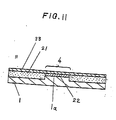
numeral 1 denotes an electrically conducting layer, 22 denotes an electrically insulating layer which is formed as a thin film, 21 denotes an electrically insulating layer, 33 denotes a metal layer which is formed as a thin film, and 4 denotes an electron emission region of themetal layer 33 With this embodiment of an electron emission element, theconducting layer 1 is formed with an upwardly protruding portion 1a, over which is formed the thin insulatinglayer 22. In addition, the insulatinglayer 21 is formed on regions of theconducting layer 1 outside of the aforementioned upwardly protruding portion 1a of theconducting layer 7, with the upper surface of the insulatinglayer 21 being coplanar with the upper surface of the insulatinglayer 22. Themetal layer 33 is formed as a continuous layer over the insulatinglayer 22 and insulatinglayer 21. When a voltage is applied by connecting themetal layer 33 to a positive potential and theconducting layer 1 to a negative potential, a strong electric field is formed in the insulatinglayer 22, immediately below theelectron emission region 4. Electrons are thereby drawn out of theconducting layer 1, and as a result of the tunnelling phenomenon within the insulatinglayer 22, the electrons pass into themetal layer 33. Those electrons which have an energy that is greater than the work function of themetal layer 33 are emitted from theelectron emission region 4. - With this embodiment, due to the fact that the interface between the insulating
layer 22 and themetal layer 33 is a single plane, without any step changes in height or thickness of these layers, the insulatinglayer 22 andmetal layer 33 can easily be formed as a respective uniform thin films, so that stable electron emission characteristics can be obtained. In addition, if an array consisting of a plurality of such electron emission elements is formed, then uniformity of electrical characteristics for the respective electron emission elements of the array can be ensured. - A method of manufacture for such an electron emission element will be described referring to Figs 12A to 12G. Firstly, a layer of a metal such as Al or Ta is formed by a process such as resistive heating evaporative deposition, electron beam evaporative deposition, or sputtering deposition, to a thickness of 0.1 to 1µm approximately, upon a surface of a
glass substrate 5, to thereby form an electrically conducting layer 1 (Fig 12A). Next, a layer ofphotoresist 7 is formed by the usual photolithographic process on the insulating layer 1 (Fig. 12B) . Etching of theconducting layer 1 is then executed to a depth d, where d is for example 0.05 to 0.5µm approximately. This etching is performed by a process such as ion milling or wet etching. (Step 12C). A layer of an electrically insulating material such as SiO₂ , Al₂O₃, or Ta₂O₅, is then formed overall, to a thickness which is equal to the depth d. This layer is formed by a process such as electron beam evaporative deposition or sputtering deposition (Fig. 12D). Thephotoresist layer 7 is then removed (Fig. 12E). Next, thermal oxidation in an oxygen atmosphere, or anodic oxidation is executed to form a film of a material such as Al₂O₃ or Ta₂O₅ as the thin insulatinglayer 22. This film is formed to a thickness t, where t is for example 50 to 200 A approximately (Fig. 12F). Themetal layer 33 is then formed on the surfaces of the insulatinglayers - The above description has been given for the case in which a substrate is provided below the conducting material. However identical results can be obtained with the invention without utilizing a substrate.
- An eighth embodiment of an electron emission element according to the present invention will be described, referring to the general cross-sectional view of Fig. 13, in which
numeral 5 denotes a substrate, 1 denotes an electrically conducting layer, 21 denotes an electrically insulating layer, 22 denotes a thin-film electrically insulating layer, 33 denotes a thin-film metal layer. The method of manufacture of such an electron emission element is as follows. Theconducting layer 1 is formed on a predetermined region of thesubstrate 5, the thin insulatinglayer 22 is then formed on theconducting layer 1, and the insulatinglayer 21 is formed on a specific region of thesubstrate 5 other than the region in which theconducting layer 1 is formed. The insulatinglayer 21 is formed such that the upper surface thereof is co-planar with the upper surface of the thin insulatinglayer 22. Athin metal layer 33 is then formed over both the insulatinglayers - It should be noted that it would be equally possible to make the value of the thickness d (in the manufacturing steps of Figs. 12C and 12D above) identical to the original thickness of the
conducting layer 1. If this is done, and the identical steps of Figs. 12A to 12G are utilized, then an electron emission element having uniform electron emission distribution over the electron emission region and stability of operation can be produced. - Furthermore although the above process has been described for the case of a single electron emission element being manufactured, it would be equally possible to similarly manufacture an array of a plurality of electron emission elements in this way, with similar results being obtained.
- With the seventh and eighth embodiments described above, the respective upper surfaces of the thin first insulating
layer 22 and the second insulatinglayer 21 are co-planar, with no step changes in height. Thus, thethin metal layer 33 that is formed thereon is completely flat and of uniform thickness. As a result, the formation of internal defects in themetal layer 33 can be prevented, so that high reliability and stability of operation is obtained. If an array of such electron emission elements is manufactured by the above process, a high degree of uniformity of characteristics of the respective elements of the array can be obtained, together with a high degree of electron emission efficiency. - Fig. 14 shows a general cross-sectional view of a ninth embodiment of an electron emission element according to the present invention. The configuration of this electron emission element is: conducting layer (conducting material) 1 - insulating layer 21 -
metal layer 33. Theconducting layer 1 has an upwardly protruding portion 1a. The insulatinglayer 21, which is sandwiched between the conductinglayer 1 and themetal layer 33, is formed such that an upper surface thereof extends over both the upwardly protruding portion 1a of theconducting layer 1 and the remaining region of theconducting layer 1. The upwardly protruding portion 1a corresponds in position to anelectron emission region 4. - When a voltage is applied such that the
conducting layer 1 is connected to a negative potential and themetal layer 33 to a positive potential, a strong electric field is produced in the thin insulatinglayer 21, below theelectron emission region 4. As a result, electrons are drawn out of theconducting layer 1 and pass through the insulatinglayer 21 by the tunnelling phenomenon. Those electrons which have an energy that is greater than the work function of themetal layer 33 are emitted from themetal layer 33, in theelectron emission region 4. - Fig. 15 shows a general cross-sectional view of a tenth embodiment of an electron emission element according to the present invention, whose configuration is : conducting layer (conducting material) conducting layer 1 - insulating
layers 21, 22 -metal layer 33. Specifically, the insulating layer that is sandwiched between the conductinglayer 1 and themetal layer 33 has an upper surface that covers all of theconducting layer 1 other than the upwardly protruding portion 1a The first insulatinglayer insulating layer 21 has an upper surface that is co-planar with the upper surface of the upwardly protruding portion 1a. The second insulatinglayer 22, which is formed such as to extend over both the upwardly protruding portion 1a and the insulatinglayer 21, has a flat upper surface. Theelectron emission region 4 is defined by the upwardly protruding portion 1a. The remaining features of this embodiment are identical to those of the ninth embodiment described above, so that further description will be omitted. - When a voltage is applied such that the
conducting layer 1 is connected to a negative potential and themetal layer 33 to a positive potential, a strong electric field is produced in the thin second insulatinglayer 22, below theelectron emission region 4. As a result, electrons are drawn out of theconducting layer 1 and pass through the second insulatinglayer 22 by the tunnelling phenomenon. Those electrons which have an energy that is greater than the work function of themetal layer 33 are emitted from themetal layer 33, in theelectron emission region 4. - With the electron emission element embodiments of Figs. 14 and 15, the
metal layer 33 is formed over an electrically insulating layer (21 or 22) having a flat surface. Themetal layer 33 is thereby formed with a flat surface, and of uniform thickness. As a result, the formation of internal defects in themetal layer 33 can be prevented, so that high reliability of electrical conduction within that layer and stability of electron emission are obtained. - A method of manufacture for the embodiment of an electron emission element of Fig. 15 will be described, referring to Figs. 16A to 16G. Firstly, an
electrically conducting layer 1 is formed as shown in Fig. 16A, by evaporative deposition of a metal upon a surface of an electrically insulating substrate 5 (consisting of a material such as glass) . The evaporative deposition can be performed by a process such as resistive heating evaporative deposition, electron beam evaporative deposition, sputtering deposition, CVD, MBE or ion beam deposition. Theconducting layer 1 can be formed of a metal such as Au, Al, Pt, Mo, Ta, Ag, W, Cr, etc, to a thickness of 0.1 to 1µm approximately. - Next, as shown in Fig. 16B, a layer of
photoresist 7 is formed selectively on a portion of theconducting layer 1 that corresponds to the electron emission region. Thephotoresist 7 is formed by the usual photo-lithography method. - After forming the
photoresist layer 7, etching of theconducting layer 1 to a depth d of, for example, 0.05 to 0.5µm is executed, in a region of theconducting layer 1 surface which is not covered by the photoresist. The etching can be performed by a process such as ion milling or wet etching. As a result, as shown in Fig. 16C, the upwardly protruding portion 1a of theconducting layer 1 is formed. - Next, as shown in Fig. 16D the first insulating layer is formed overall, with a thickness which is equal to the aforementioned depth d, so that an upper surface of this first insulating
layer 21 is co-planar with the upper surface of the upwardly protruding portion 1a. The first insulatinglayer 21 is formed by a process such as electron beam evaporative deposition, sputtering deposition, CVD, MBE or ion beam deposition, and consisting of a material such as SiO₂, Al₂O₃, Ta₂O₅, SiNx, BN, AlN, C, etc. - After forming the first insulating
layer 21, as shown in Fig. 16E, thephotoresist layer 7 is removed. Next, (as shown in Fig. 16F) the upper surface of the first insulatinglayer 21 and the upwardly protruding portion 1a have the second insulatinglayer 22 formed thereon, to a thickness of 50 to 200 Å approximately. The second insulatinglayer 22 can be formed by a method such as electron beam evaporative deposition, sputtering deposition, CVD, MBE, or ion beam deposition, and consisting of a material such as SiO₂, Al₂O₃, Ta₂O₅, SiNx, BN, AlN, C, etc. - Finally, as shown in Fig. 16G, the
metal layer 33 is formed as a layer of Au, Al, Mo, W, etc, over the flat surface of the second insulatinglayer 22, to thereby complete the formation of the electron emission element. Themetal layer 33 is formed by a process such as resistive heating evaporative deposition, vacuum evaporative deposition, CVD, MBE, ion beam deposition, etc, and is preferably formed to a thickness of 50 to 200 Å. - As can be understood from the above description, the upwardly protruding portion 1a of the insulating
layer 1 defines theelectron emission region 4. The upwardly protruding portion 1a can be formed to any desired shape, by a process such as etching, and hence the shape of an electron beam that is formed of the electrons produced from the electron emission region can be made of any arbitrary form. - Fig. 17 shows a general cross-sectional view of an eleventh embodiment of an electron emission element according to the present invention. The configuration of this electron emission is basically: electrically insulating substrate 5 - electrically conducting layer (or conducting body) 1 - electrically insulating layer 21 -
metal layer 33. Theconducting layer 1 is formed on a region of the insulatingsubstrate 5, of specific shape and position. The insulatinglayer 21 that is sandwiched between the conductinglayer 1 and themetal layer 33 is configured such as to cover both a region of the surface of the insulatingsubstrate 5 that is not covered by theconducting layer 1 and also the surface of theconducting layer 1, and is formed with a flat upper surface. The upper surface of theconducting layer 1 defines the shape and position of theelectron emission region 4. - When a voltage is applied such that the
conducting layer 1 is connected to a negative potential and themetal layer 33 to a positive potential, a strong electric field is produced in a thin film portion of the insulatinglayer 21 which is immediately below theelectron emission region 4 of themetal layer 33. As a result, electrons are drawn out of theconducting layer 1 and pass through the insulatinglayer 21 by the tunnelling phenomenon. Those electrons which have an energy that is greater than the work function of themetal layer 33 are emitted fromelectron emission region 4 of themetal layer 33. - Fig. 18 shows a general cross-sectional view of a twelfth embodiment of an electron emission element according to the present invention. With this electron emission element embodiment, the configuration is basically: insulating substrate 31 - electrically conducting layer 1 - electrically
insulating layers 21, 22 -metal layer 33. The insulating layers that are sandwiched between the conductinglayer 1 and themetal layer 33 consist of a first insulatinglayer 21 which covers a region of thesubstrate 31 that is not covered by theconducting layer 1 and which has an upper surface that is co-planar with the upper surface of theconducting layer 1, and a second insulatinglayer 22 which covers the upper surfaces of both the first insulatinglayer 21 and theconducting layer 1. Theelectron emission region 4 is defined by the area of intersection between the conductinglayer 1 and themetal layer 33. The remaining features of this embodiment are identical to those of the embodiment of Fig. 17 above, and further description will be omitted. - When a voltage is applied such that the
conducting layer 1 is connected to a negative potential and themetal layer 33 to a positive potential, a strong electric field is produced in the portion of the thin second insulatinglayer 22, below theelectron emission region 4. As a result, electrons are drawn out of theconducting layer 1 and pass through the second insulatinglayer 22 by the tunnelling phenomenon. Those electrons which have an energy that is greater than the work function of themetal layer 33 are emitted from theelectron emission region 4 of themetal layer 33. - With the electron emission element embodiments of Figs. 17 and 18, as for the embodiments of Figs. 14 and 15, the
metal layer 33 is formed over a flat upper surface of the insulatinglayers metal layer 33 can be made of precisely uniform thickness, with no variations in height, so that a high degree of reliability of electrical conduction within that metal layer is obtained. - Furthermore, with the embodiments of Figs. 17 and 18, the
conducting layer 1 that is formed on a region of a surface of thesubstrate 5 defines the shape and position of theelectron emission region 4. Since the shape (i.e. as seen in plan) of theconducting layer 1 can be freely selected, any arbitrary shape can be selected for an electron beam that is formed from the electrons that are emitted from the electron emission region. - It has been found from measurements made on each of the embodiments of Figs. 14 through 17 that, in each case, the shape of a beam spot of an electron beam obtained from the electron emission element corresponds to the shape of the electron emission region of that electron emission element.
- Furthermore with each of the embodiments of Figs. 14 through 17, it would be possible to form an electron emission element with a plurality of electron emission regions, arrayed in a predetermined array configuration, It has been found that if such an array configuration is utilized, the various advantages described hereinabove are still obtained.
- Moreover for each of the embodiment of Figs. 15 and 18, instead of forming the second insulating
layer 22 by deposition of a layer of electrically insulating material after forming the first insulatinglayer 21, it would be equally possible to form an electrically insulating oxide film by oxidation of a surface portion of theconducting layer 1, and to form themetal layer 33 over this insulating oxide film and the first insulatinglayer 21. - It should also be noted that it is not essential that the
metal layer 33 be formed above the entire upper surface of the upwardly protruding portion 1a of theconducting layer 1, and that it would be equally possible to arrange that themetal layer 33 is formed over only a portion of the upwardly protruding portion 1a. In that case, the electron emission region would be defined by the region of intersection of the upwardly protruding portion 1a and themetal layer 33, as viewed in plan. - With each of the embodiments of Figs. 11 through 18 described above, a
metal layer 33 is formed over a completely flat surface of an electrically insulating layer (21 or 22) . As a result, themetal layer 33 can be made completely flat and of uniform thickness, ensuring that a high degree of reliability of electrical conduction within that metal layer is achieved, together with stable and uniform electron emission throughout the electron emission region. Furthermore since any arbitrary shape of the electron emission region can be easily selected, the shape of the beam spot of an electron beam produced by utilizing such an electron emission element can be easily determined in accordance with a specific application. Thus these embodiments are highly practical. - An MIM type of electron emission element having a thin insulating film (2) formed below an electron emission region (4) of a metal layer (3), with that electron emission region of the metal layer consisting of an array of thick and thin portions (3a, 3b), distributed throughout the electron emission region. Improved efficiency and uniformity of of emission are obtained, due to the low resistance of the thick portions, which effectively apply a supply voltage to the thin portions of the metal layer, while the thin portions can be made sufficiently thin to maximize the electron emission level.
Claims (27)
forming a layer of an electrically conducting material on a surface of a glass substrate;
forming a layer of an electrically insulating material on said conducting material;
forming a metal layer upon said layer of insulating material;
forming a patterned photoresist layer on said metal layer; and
executing photo-lithography etching of said metal layer, employing said photoresist layer, to selectively remove portions of said metal layer.
forming a layer of an electrically insulating material on a region of a conducting body corresponding to an electron emission region, the thickness of said layer of insulating material being selected such as to permit an electron tunnelling effect to occur in said layer of insulating material; and
executing evaporative deposition of a metal onto a surface of said insulating layer through a mask, said mask having a predetermined pattern of apertures formed therein, and said mask being spaced apart from said layer of insulating material by a predetermined distance;
for thereby forming a plurality of thick portions and a plurality of sloping portions of said metal layer within said electron emission region, each of said sloping portions being integrally formed with a corresponding one of said thick portions and being of gradually varying thickness, said thick portions and sloping portions being distributed throughout said electron emission region.
Applications Claiming Priority (10)
| Application Number | Priority Date | Filing Date | Title |
|---|---|---|---|
| JP63274852A JPH02121227A (en) | 1988-10-31 | 1988-10-31 | Electron emission element and manufacture thereof |
| JP274852/88 | 1988-10-31 | ||
| JP63278702A JPH02126531A (en) | 1988-11-04 | 1988-11-04 | Electron emission element |
| JP63278707A JPH02126532A (en) | 1988-11-04 | 1988-11-04 | Electron emission element |
| JP278707/88 | 1988-11-04 | ||
| JP278702/88 | 1988-11-04 | ||
| JP324107/88 | 1988-12-22 | ||
| JP63324107A JPH02170327A (en) | 1988-12-22 | 1988-12-22 | Electron releasing element |
| JP326613/88 | 1988-12-23 | ||
| JP63326613A JPH02172127A (en) | 1988-12-23 | 1988-12-23 | Electron emission element and its manufacture |
Publications (2)
| Publication Number | Publication Date |
|---|---|
| EP0367195A2 true EP0367195A2 (en) | 1990-05-09 |
| EP0367195A3 EP0367195A3 (en) | 1991-10-02 |
Family
ID=27530596
Family Applications (1)
| Application Number | Title | Priority Date | Filing Date |
|---|---|---|---|
| EP19890120124 Withdrawn EP0367195A3 (en) | 1988-10-31 | 1989-10-30 | Mim cold-cathode electron emission elements and methods of manufacture thereof |
Country Status (2)
| Country | Link |
|---|---|
| US (1) | US5202605A (en) |
| EP (1) | EP0367195A3 (en) |
Cited By (11)
| Publication number | Priority date | Publication date | Assignee | Title |
|---|---|---|---|---|
| EP0394698A2 (en) * | 1989-03-30 | 1990-10-31 | Canon Kabushiki Kaisha | Electron beam lithography machine and image display apparatus |
| EP0878819A2 (en) * | 1997-05-15 | 1998-11-18 | Pioneer Electronic Corporation | Electron emission device and display device using the same |
| EP0878820A2 (en) * | 1997-05-15 | 1998-11-18 | Pioneer Electronic Corporation | Electron emission device and display device using the same |
| WO1999065050A1 (en) * | 1998-06-11 | 1999-12-16 | Petr Viscor | Planar electron emitter (pee) |
| EP1117118A1 (en) * | 2000-01-13 | 2001-07-18 | Pioneer Corporation | Electron-emitting device and method of manufacturing the same and display apparatus using the same |
| EP1117117A1 (en) * | 2000-01-14 | 2001-07-18 | Pioneer Corporation | Image pickup device including electron-emitting devices |
| EP1220279A2 (en) * | 2000-12-28 | 2002-07-03 | Pioneer Corporation | Flat panel display device utilizing electron emission devices |
| EP1251503A2 (en) * | 2001-04-16 | 2002-10-23 | Hewlett-Packard Company | Data storage device |
| EP1302964A1 (en) * | 2001-10-12 | 2003-04-16 | Hewlett-Packard Company | Field-enhanced MIS/MIM electron emitters |
| US6872964B2 (en) | 2003-08-20 | 2005-03-29 | Hewlett-Packard Development Company, L.P. | Data storage device |
| EP1523025B1 (en) * | 2002-03-25 | 2012-12-19 | Panasonic Corporation | Field emission-type electron source |
Families Citing this family (6)
| Publication number | Priority date | Publication date | Assignee | Title |
|---|---|---|---|---|
| GB9702348D0 (en) * | 1997-02-05 | 1997-03-26 | Smiths Industries Plc | Electron emitter devices |
| JP3765671B2 (en) * | 1998-08-10 | 2006-04-12 | パイオニア株式会社 | Electron emission device and electron emission display device using the same |
| JP3863325B2 (en) * | 1999-09-10 | 2006-12-27 | 株式会社日立製作所 | Image display device |
| US6738336B2 (en) * | 2001-05-16 | 2004-05-18 | Hewlett-Packard Development Company, L.P. | Data storage device |
| US20050017624A1 (en) * | 2003-07-23 | 2005-01-27 | Thomas Novet | Electron emitter with epitaxial layers |
| DE102010043277A1 (en) | 2010-11-03 | 2012-05-03 | Robert Bosch Gmbh | Microelectromechanical sensor for measuring a force and corresponding method |
Citations (3)
| Publication number | Priority date | Publication date | Assignee | Title |
|---|---|---|---|---|
| US3184636A (en) * | 1961-06-15 | 1965-05-18 | Sylvania Electric Prod | Cold cathode |
| FR1572047A (en) * | 1967-07-25 | 1969-06-20 | ||
| DE1589822A1 (en) * | 1967-04-26 | 1970-03-26 | Gentsch Dr Horst | Emitter diode for generating ions and free electrons |
Family Cites Families (8)
| Publication number | Priority date | Publication date | Assignee | Title |
|---|---|---|---|---|
| US3325733A (en) * | 1960-12-27 | 1967-06-13 | Jerome H Lemelson | Measuring device using variable thickness thin film tunneling layer |
| DE1252818B (en) * | 1962-03-22 | 1900-01-01 | ||
| US3184659A (en) * | 1962-08-13 | 1965-05-18 | Gen Telephone & Elect | Tunnel cathode having a metal grid structure |
| US3447043A (en) * | 1966-12-29 | 1969-05-27 | Itt | Tunnel cathode in matrix form with integral storage feature |
| JPS62272421A (en) * | 1986-05-20 | 1987-11-26 | Canon Inc | Electron emitting element |
| JPH0736453B2 (en) * | 1986-06-11 | 1995-04-19 | 株式会社リコー | Metal-insulator-metal element |
| JPH0797475B2 (en) * | 1986-06-25 | 1995-10-18 | キヤノン株式会社 | Electron-emitting device |
| JPS636717A (en) * | 1986-06-26 | 1988-01-12 | Canon Inc | Electron-emitting device |
-
1989
- 1989-10-30 EP EP19890120124 patent/EP0367195A3/en not_active Withdrawn
- 1989-10-31 US US07/429,526 patent/US5202605A/en not_active Expired - Fee Related
Patent Citations (3)
| Publication number | Priority date | Publication date | Assignee | Title |
|---|---|---|---|---|
| US3184636A (en) * | 1961-06-15 | 1965-05-18 | Sylvania Electric Prod | Cold cathode |
| DE1589822A1 (en) * | 1967-04-26 | 1970-03-26 | Gentsch Dr Horst | Emitter diode for generating ions and free electrons |
| FR1572047A (en) * | 1967-07-25 | 1969-06-20 |
Non-Patent Citations (2)
| Title |
|---|
| JOURNAL OF APPLIED PHYSICS, Vol. 45, No. 1, January 1974, Pages 119-125, New York, US; D.G. ONN et al.: "Cryogenic thin-film electron emitters". * |
| ZEITSCHRIFT FÜR NATURFORSCHUNG, part A, Vol. 26, No. 6, June 1971, Pages 1010-1016, Tübingen, DE; H. GENTSCH et al.: "MOS-Sandwich-Gitter-Diode zur Erzeugung von Feldionisationsfeldstärken ander Phasengrenze Festkörper/Gas". * |
Cited By (22)
| Publication number | Priority date | Publication date | Assignee | Title |
|---|---|---|---|---|
| EP0394698A3 (en) * | 1989-03-30 | 1991-10-02 | Canon Kabushiki Kaisha | Electron beam lithography machine and image display apparatus |
| US5569974A (en) * | 1989-03-30 | 1996-10-29 | Canon Kabushiki Kaisha | Electron-emitting device and electron beam lithograph machine and image display apparatus making use of it |
| EP0394698A2 (en) * | 1989-03-30 | 1990-10-31 | Canon Kabushiki Kaisha | Electron beam lithography machine and image display apparatus |
| EP0878819A2 (en) * | 1997-05-15 | 1998-11-18 | Pioneer Electronic Corporation | Electron emission device and display device using the same |
| EP0878820A2 (en) * | 1997-05-15 | 1998-11-18 | Pioneer Electronic Corporation | Electron emission device and display device using the same |
| EP0878819A3 (en) * | 1997-05-15 | 1998-12-09 | Pioneer Electronic Corporation | Electron emission device and display device using the same |
| EP0878820A3 (en) * | 1997-05-15 | 1998-12-09 | Pioneer Electronic Corporation | Electron emission device and display device using the same |
| US6147443A (en) * | 1997-05-15 | 2000-11-14 | Pioneer Electronic Corporation | Electron emission device and display device using the same |
| AU755927B2 (en) * | 1998-06-11 | 2003-01-02 | Armin Delong | Planar electron emitter (PEE) |
| WO1999065050A1 (en) * | 1998-06-11 | 1999-12-16 | Petr Viscor | Planar electron emitter (pee) |
| US7399987B1 (en) | 1998-06-11 | 2008-07-15 | Petr Viscor | Planar electron emitter (PEE) |
| EP1117118A1 (en) * | 2000-01-13 | 2001-07-18 | Pioneer Corporation | Electron-emitting device and method of manufacturing the same and display apparatus using the same |
| EP1117117A1 (en) * | 2000-01-14 | 2001-07-18 | Pioneer Corporation | Image pickup device including electron-emitting devices |
| US6744063B2 (en) | 2000-01-14 | 2004-06-01 | Pioneer Corporation | Image pickup device including electron-emitting devices |
| EP1220279A3 (en) * | 2000-12-28 | 2006-03-22 | Pioneer Corporation | Flat panel display device utilizing electron emission devices |
| EP1220279A2 (en) * | 2000-12-28 | 2002-07-03 | Pioneer Corporation | Flat panel display device utilizing electron emission devices |
| EP1251503A2 (en) * | 2001-04-16 | 2002-10-23 | Hewlett-Packard Company | Data storage device |
| EP1251503A3 (en) * | 2001-04-16 | 2004-09-08 | Hewlett-Packard Company | Data storage device |
| EP1302964A1 (en) * | 2001-10-12 | 2003-04-16 | Hewlett-Packard Company | Field-enhanced MIS/MIM electron emitters |
| US6822380B2 (en) | 2001-10-12 | 2004-11-23 | Hewlett-Packard Development Company, L.P. | Field-enhanced MIS/MIM electron emitters |
| EP1523025B1 (en) * | 2002-03-25 | 2012-12-19 | Panasonic Corporation | Field emission-type electron source |
| US6872964B2 (en) | 2003-08-20 | 2005-03-29 | Hewlett-Packard Development Company, L.P. | Data storage device |
Also Published As
| Publication number | Publication date |
|---|---|
| US5202605A (en) | 1993-04-13 |
| EP0367195A3 (en) | 1991-10-02 |
Similar Documents
| Publication | Publication Date | Title |
|---|---|---|
| US5202605A (en) | Mim cold-cathode electron emission elements | |
| US5556316A (en) | Clustered field emission microtips adjacent stripe conductors | |
| EP0495436B1 (en) | Quantum phase interference transistor | |
| US5541466A (en) | Cluster arrangement of field emission microtips on ballast layer | |
| US6281621B1 (en) | Field emission cathode structure, method for production thereof, and flat panel display device using same | |
| US5394006A (en) | Narrow gate opening manufacturing of gated fluid emitters | |
| US5569975A (en) | Cluster arrangement of field emission microtips | |
| JPH0636680A (en) | Electronic element using diamond film electron source | |
| US5378182A (en) | Self-aligned process for gated field emitters | |
| US5502314A (en) | Field-emission element having a cathode with a small radius | |
| US5847496A (en) | Field emission device including a resistive layer | |
| KR100750411B1 (en) | Devices with graded top oxide and graded drift region | |
| US5717278A (en) | Field emission device and method for fabricating it | |
| US5557159A (en) | Field emission microtip clusters adjacent stripe conductors | |
| US6084245A (en) | Field emitter cell and array with vertical thin-film-edge emitter | |
| US5791961A (en) | Uniform field emission device | |
| JPH0217676A (en) | Semiconductor device | |
| JP3033178B2 (en) | Field emission type emitter | |
| JPH09246521A (en) | Method of manufacturing and connecting microminiature semiconductor device | |
| JP3539305B2 (en) | Field emission type electron source and method of manufacturing the same | |
| EP0713236A1 (en) | Electron emission apparatus | |
| JPH03295130A (en) | Electron emission device | |
| JPH03230446A (en) | Electron emitting element and manufacture thereof | |
| JPH02172127A (en) | Electron emission element and its manufacture | |
| JP3436288B2 (en) | Method of forming electrode structure |
Legal Events
| Date | Code | Title | Description |
|---|---|---|---|
| PUAI | Public reference made under article 153(3) epc to a published international application that has entered the european phase |
Free format text: ORIGINAL CODE: 0009012 |
|
| 17P | Request for examination filed |
Effective date: 19891030 |
|
| AK | Designated contracting states |
Kind code of ref document: A2 Designated state(s): DE FR GB |
|
| PUAL | Search report despatched |
Free format text: ORIGINAL CODE: 0009013 |
|
| AK | Designated contracting states |
Kind code of ref document: A3 Designated state(s): DE FR GB |
|
| 17Q | First examination report despatched |
Effective date: 19930928 |
|
| STAA | Information on the status of an ep patent application or granted ep patent |
Free format text: STATUS: THE APPLICATION IS DEEMED TO BE WITHDRAWN |
|
| 18D | Application deemed to be withdrawn |
Effective date: 19940209 |