EP1302964A1 - Field-enhanced MIS/MIM electron emitters - Google Patents
Field-enhanced MIS/MIM electron emitters Download PDFInfo
- Publication number
- EP1302964A1 EP1302964A1 EP02257067A EP02257067A EP1302964A1 EP 1302964 A1 EP1302964 A1 EP 1302964A1 EP 02257067 A EP02257067 A EP 02257067A EP 02257067 A EP02257067 A EP 02257067A EP 1302964 A1 EP1302964 A1 EP 1302964A1
- Authority
- EP
- European Patent Office
- Prior art keywords
- insulator
- electron
- electron supply
- protrusion
- emitter
- Prior art date
- Legal status (The legal status is an assumption and is not a legal conclusion. Google has not performed a legal analysis and makes no representation as to the accuracy of the status listed.)
- Withdrawn
Links
Images


Classifications
-
- H—ELECTRICITY
- H01—ELECTRIC ELEMENTS
- H01J—ELECTRIC DISCHARGE TUBES OR DISCHARGE LAMPS
- H01J1/00—Details of electrodes, of magnetic control means, of screens, or of the mounting or spacing thereof, common to two or more basic types of discharge tubes or lamps
- H01J1/02—Main electrodes
- H01J1/30—Cold cathodes, e.g. field-emissive cathode
- H01J1/312—Cold cathodes, e.g. field-emissive cathode having an electric field perpendicular to the surface, e.g. tunnel-effect cathodes of Metal-Insulator-Metal [MIM] type
-
- B—PERFORMING OPERATIONS; TRANSPORTING
- B82—NANOTECHNOLOGY
- B82Y—SPECIFIC USES OR APPLICATIONS OF NANOSTRUCTURES; MEASUREMENT OR ANALYSIS OF NANOSTRUCTURES; MANUFACTURE OR TREATMENT OF NANOSTRUCTURES
- B82Y10/00—Nanotechnology for information processing, storage or transmission, e.g. quantum computing or single electron logic
Definitions
- This invention relates generally to field enhanced Metal-Insulator-Semiconductor (MIS) or Metal-Insulator-Metal (MIM) electron emitter devices, hereinafter collectively referred to as FEMIS and to methods for fabricating such devices.
- MIS Metal-Insulator-Semiconductor
- MIM Metal-Insulator-Metal
- Electron emission technology exists in many forms today.
- cathode ray tubes CRT
- CTR cathode ray tubes
- Electron emission plays a critical role in devices such as x-ray machines and electron microscopes.
- microscopic cold cathodes can be employed in electron-beam lithography used, for example, in making integrated circuits, in information storage devices such as those described in Gibson et al, U.S. Patent 5,557,596, in microwave sources, in electron amplifiers, and in flat panel displays. Actual requirements for electron emission vary according to application.
- electron beams need to deliver sufficient current, be as efficient as possible, operate at application-specific voltages, be focusable, be reliable at the required power densities, and be stable both spatially and temporally at a reasonable vacuum for any given application.
- Portable devices for example, demand low power consumption.
- MIS Metal-Insulator-Semiconductor
- MIM Metal-Insulator-Metal
- Iwasaki, et al U.S. Patent 6,066,922.
- electrons are 1) injected into the insulator layer from the electron supply layer (metal or semiconductor), 2) accelerated in the insulator layer, 3) injected into the thin metal top electrode, and 4) emitted from the surface of the thin metal top electrode.
- MIS Metal-Insulator-Semiconductor
- MIM Metal-Insulator-Metal
- Shortcomings of MIS or MIM devices include relatively low emission current densities (typically about 1 to 10 mA/cm 2 ) and poor efficiencies (defined as the ratio of emitted current to shunt current between the electron supply layer and the thin metal electrode) (typically approximately 0.1 %).
- Electrons may also be emitted from conducting or semiconducting solids into a vacuum through an application of an electric field at the surface of the solid.
- This type of electron emitter is commonly referred to as a field emitter.
- Emitted electrons from field emitters possess no kinetic energy at the surface of the solid.
- the process for making tip-shaped electron field emitters, hereinafter referred to as Spindt emitters is described in C. A. Spindt, et al, "Physical Properties of Thin-Film Field Emission Cathodes with Molybdenum Cones", Journal of Applied Physics, vol. 47, No. 12, December 1976, pp. 5248-5263.
- the electron-emitting surface is shaped into a tip in order to induce a stronger electric field at the tip surface for a given potential between the tip surface and an anode; the sharper the tip, the lower the potential necessary to extract electrons from the emitter.
- the shortcomings of Spindt emitters include requiring a relatively hard vacuum (pressure ⁇ 10 -6 Torr, preferably ⁇ 10 -8 Torr) to provide both spatial and temporal stability as well as reliability. Furthermore, the angle of electron emission is relatively wide with Spindt emitters making emitted electron beams relatively more difficult to focus to spot sizes required for electron-beam lithography or information storage applications. Operational bias voltages for simple Spindt tips are relatively high, ranging up to 1000 volts for a tip-to-anode spacing of 1 millimeter.
- an embodiment of a FEMIS electron emitter may include an electron supply structure.
- the electron supply structure is such that at least one protrusion, preferably a plurality of protrusions, may be formed on a top side of the electron supply structure.
- the electron supply structure may be formed from a conductive substrate and optionally an electron supply layer formed above the conductive substrate.
- the electron emitter may also include an insulator formed above the electron supply structure and protrusion(s). In this manner, any given protrusion becomes internal to the electron emitter structure.
- the electron emitter may further include a top conductive layer formed above the insulator.
- the FEMIS electron emitter may be such that a portion of the insulator above any given protrusion is thinner than a portion of the insulator that is above the relatively flat region of the electron supply structure. Additionally the insulator may be shaped to curve inward on both lower and upper sides near any given protrusion, i.e., the insulator may be hourglass-shaped locally. The insulator can also be substantially conformal to the electron supply layer, i.e., have the shape of the surface of the electron supply layer including protrusions prior to the formation of the insulator.
- an embodiment of a method of forming an FEMIS electron emitter may include forming an electron supply structure.
- the electron supply structure is such that at least one protrusion, preferably a plurality of protrusions, may be formed on a top side of the electron supply structure.
- the electron supply structure may be formed from a conductive substrate and optionally from an electron supply layer formed above the conductive layer substrate.
- the method may also include forming an insulator above the electron supply structure and protrusion(s). In this manner, any given protrusion becomes internal to the electron emitter structure.
- the method may further include forming a top conductive layer above the insulator.
- Certain embodiments of the present invention may be capable of achieving certain aspects. For example, because any given protrusion is internal to the emitter structure, it is not exposed to vacuum. Thus, the emitter is relatively insensitive to the contaminants that may exist in the vacuum, a situation that helps to prolong the life and efficiency of the emitter as well as to promote the spatial and temporal stability of the electron beam emitted. Consequently, vacuum requirements can be substantially relaxed.
- any given protrusion coupled with a relatively thin insulator gives rise to an enhanced electric field at that protrusion when a voltage is applied between the conductive substrate and the top conductive layer.
- Relatively low operational voltages are therefore possible with FEMIS electron emitters.
- the electric field away from any given protrusion is relatively low thereby improving the reliability of the entire emitter structure.
- Current densities and efficiencies from FEMIS electron emitters can be relatively high.
- the electron beam from a FEMIS emitter is also relatively easy to focus.
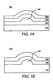
- Figs. 1A and 1B illustrate cross sections of first and second embodiments of an exemplary FEMIS electron emitter 100 according to an aspect of the present invention.
- the electron emitter 100 may include a conductive substrate 110.
- the conductive substrate 110 may be formed from metal (aluminum, tungsten, titanium, copper, gold, tantalum, platinum, iridium, palladium, rhodium, chromium, magnesium, scandium, yttrium, vanadium, zirconium, niobium, molybdenum, silicon, beryllium, hafnium, silver, and osmium and any alloys, and multilayered films thereof); doped polysilicon; doped silicon; graphite; metal-coated glass, ceramic, or plastic; indium-tin-oxide (ITO) coated glass, ceramic, or plastic; and the like.
- the metal or ITO coatings may be patterned or unpattemed.
- the top surface of the conductive substrate may be planarized
- the electron emitter 100 may also include an electron supply layer 120 as shown in Fig. 1A. As shown in Fig. 1B, the electron supply layer 120 is not necessary to practice the invention.
- a protrusion 130 may be formed on a top side of the electron supply layer 120 (see Fig. 1A) or on a top side of the conductive substrate 110 (see Fig. 1B). There may be many of these protrusions 130 included in the electron emitter 100. The sharpness of any given protrusion 130 may be controlled in the fabrication process. As a result, the current output per protrusion 130 may be obtained at relatively lower voltages according to Fowler-Nordheim emission statistics.
- the density of the protrusions 130 may also be controlled. For example, densities of several hundred protrusions 130 per square micrometer can be obtained. Consequently the total emission current can be controlled. Since any given protrusion 130 may be capable of delivering a given current in the limit, higher current may be delivered by increasing the number of protrusions 130 per emission area. Since the current can be related to voltage applied between the conductive substrate 110 and a top conductive layer 150 through the Fowler-Nordheim equation, control voltages, hence power, can be adjusted downward depending upon application.
- the electron supply layer 120 including the protrusion(s) 130 of the electron emitter 100, may be formed from a semiconductor, such as polysilicon, that may or may not be doped.
- the polysilicon may be undoped. If n-type doping is preferable, the level of doping along a depth of the electron supply layer 120 may be varied to tailor electron transport. In addition, the doping may be confined to given areas through the use of masks.
- the formation of the protrusion(s) 130 may be accomplished through the growth of hemispherical grain (HSG) polysilicon as part of the process in forming the polysilicon comprising the electron supply layer 120 or the conductive substrate 110.
- the growth of protrusion(s) 130 may be effected by seeding the growth of HSG polysilicon in subsequent processes.
- HSG polysilicon is described in M. Yoshimaru, et al, "Rugged surface poly-Si electrode and low temperature deposited Si3N4 for 64 Mbit and beyond STC DRAM cell", Tech. Digest, 1990 International Electron Devices Meeting, San Francisco, December 9-12, 1990, paper 27.4, pp. 659-662.
- the electron emitter 100 may further include an insulator 140 formed above the electron supply layer 120 or the conductive substrate 110 including the protrusion(s) 130.
- the insulator 140 may be formed from materials such as the oxides, nitrides, and oxynitrides of silicon, aluminum, titanium, tantalum, tungsten, hafnium, zirconium, vanadium, niobium, molybdenum, chromium, yttrium, scandium, nickel, cobalt, beryllium, magnesium, and combinations thereof.
- the insulator may also be formed from diamond-like carbon. However, one of ordinary skill will realize that the list of materials is not exhaustive. Indeed, the insulator 140 may be formed by oxidizing a top portion of the electron supply layer 120.
- the insulator 140 may be formed such that the insulator 120 is substantially conformal with the electron supply layer 120 or the conductive substrate 110 including protrusion(s) 130.
- the lower bound on the thickness of the insulator 140 may be largely determined by the potential between the electron supply layer 120 and the top conductive layer 150 that is sufficient to overcome the work function of the top conductive layer 150, which is typically 4 to 6 electron volts (eV). Breakdown voltage of the insulator 140 at any given thickness and the work function of the top conductive layer 150 therefore dictate the lower bound on the thickness of the insulator 140.
- the upper bound on the thickness of the insulator 140 may be determined by the potential necessary to cause electron transport in the insulator 140. The thicker the insulator 140 is; the higher the required potential.
- the thinness of the insulator 140 near any given protrusion 130 and the shape of any given protrusion 130 allows a relatively large electric field to be generated at relatively low applied bias voltages between the conductive substrate 110 and the top conductive layer 150.
- a relatively large electric field For the example of an FEMIS emitter formed of undoped polysilicon and an insulator thickness of 25 nm, only about a 6 volt bias needs to be applied to generate a sufficient electric field to give rise to electron emission by overcoming the work function of the top conductive layer 150.
- the applied potential would be approximately 1,000 Volts.
- the electron emitter 100 may include the top conductive layer 150 formed above the insulator 140.
- the top conductive layer 150 may be formed from metal (aluminum, tungsten, titanium, molybdenum titanium, copper, gold, silver, tantalum, platinum, iridium, palladium, rhodium, chromium, magnesium, scandium, yttrium, vanadium, zirconium, niobium, molybdenum, hafnium, silver, and osmium and any alloys or multilayered films), doped polysilicon, graphite, etc. or combinations of metal and non-metal, e.g., conductive carbon, films. When exposed to air the outer surface of the top conductive layer 150 is preferred to not oxidize to an insulating native oxide.
- a bias voltage is applied between the conductive substrate 110 and the top conductive layer 150.
- electrons transported through the conductive substrate 110 (and the electron supply layer 120) tunnel through the insulator 140 near any given protrusion 130 and are emitted from the top conductive layer 150.
- Figs. 2A and 2B illustrate cross sections of third and fourth embodiments of an exemplary FEMIS electron emitter 200 according to an aspect of the present invention.
- the third and fourth embodiments may include many of the same features described herein with respect to first and second embodiments, respectively, of Figs. 1A and 1B.
- the electron emitter 200 may include a conductive substrate 210 (with at least one protrusion 230, see Fig. 2A), optionally an electron supply layer 220 with at least one protrusion 230 (see Fig. 2B), an insulator 240, and a top conductive layer 250. Only those elements distinguishable between the embodiments are described.
- the insulator 240 may be formed such that the insulator 240 near any given protrusion 230 is relatively thinner than the insulator 240 on regions of the electron supply layer 220 that are substantially flat.
- the thickness of the insulator 240 near the protrusion 130 may be between 5 - 300 nanometers (nm), but may be 30 - 325 nm thick in the substantially flat region assuming that the protrusion(s) 230 protrudes 25 nm above the substantially flat regions of the electron supply layer 220.
- the outer surface of the insulator 240 is relatively flat. Focusing of the emitted electron beam may be improved with such structure through control of electron beam divergence. The same arguments with respect to limits on the thickness of the insulator 240 above the protrusion(s) 230 still pertain.
- Figs. 3A and 3B illustrate cross sections of fifth and sixth embodiments of an exemplary FEMIS electron emitter 300 according to another aspect of the present invention.
- the fifth and sixth embodiments may include many of the same features described herein with respect to first and second embodiments, respectively, of Figs. 1A and 1B.
- the electron emitter 300 may include a conductive substrate 310 (at least one protrusion 130, see Fig. 3A), optionally an electron supply layer 320 with at least one protrusion 330 (see Fig. 3B), an insulator 340, and a top conductive layer 350. Only those elements distinguishable amongst the embodiments are described.
- the shape of the insulator 340 is such that a horizontal hourglass shape is formed near any given protrusion 330. Focusing of the emitted electron beam may be further improved with such structure.
- the same arguments with respect to limits on the thickness of the insulator 340 above the protrusion(s) 330 still pertain.
- Figs. 4A - 4C collectively illustrate a method of fabricating the first embodiment of the electron emitter 100 shown in Fig. 1A.
- the conductive substrate 110 may be formed.
- Protrusions 130 may be formed at this point as part of forming the conductive substrate 110 (not shown).
- the electron supply layer 120 may be formed above the conductive substrate 110 and the protrusion(s) 130 may be formed as part of the forming the electron supply layer 120.
- the top of the conductive substrate 110 may be planarized using commonly known techniques such as CMP prior to forming the electron supply layer 120.
- the polysilicon may be grown on the conductive substrate 110 by low pressure chemical-vapor-deposition (LPCVD).
- LPCVD low pressure chemical-vapor-deposition
- a preferred temperature when performing LPCVD is substantially between 550 C° and 620 C°.
- the preferred thickness of the polysilicon may range substantially between 0.05 ⁇ m and 1 ⁇ m.
- the polysilicon may be grown through other deposition processes such as plasma-enhanced chemical-vapor-deposition (PECVD), other CVD variations, or physical vapor deposition (PVD) techniques that include sputter deposition and evaporation.
- PECVD plasma-enhanced chemical-vapor-deposition
- PVD physical vapor deposition
- the electron supply layer 120 may be doped or undoped.
- the electron supply layer 120 such as the polysilicon, may be doped through incorporation of an n-type dopant such as phosphorous, arsenic or antimony during deposition of the polysilicon.
- an n-type dopant such as phosphorous, arsenic or antimony during deposition of the polysilicon.
- the dopant concentration may be modified over time so that different depth levels of the electron supply layer 120 have varying dopant levels.
- ion implantation and subsequent annealing may also be used for either uniform or graded dopant incorporation after the electron supply layer 120 has been formed.
- the insulator 140 may be formed above the electron supply layer 120 as shown in Fig. 4B.
- the electron supply layer 120 (or the conductive substrate 110) and the protrusion(s) 130 become substantially conformally covered, i.e., any given protrusion 130 becomes internal to the emitter structure. Any given protrusion 130 is consequently not exposed to vacuum and therefore becomes relatively insensitive to the vagaries of the vacuum environment during operation of the electron emitter. As a result, vacuum requirements are relaxed.
- the insulator 140 may be formed through oxidizing the polysilicon, for example, by rapid oxidation in a dry oxygen atmosphere at a temperature substantially ranging between 800 C° and 1000 C° and time substantially between 5 and 60 minutes.
- Other methods of oxidation include but are not limited to plasma oxidation, wet thermal oxidation, and electrochemical oxidation.
- the top conductive layer 150 may be formed above the insulator 140 to fabricate the FEMIS electron emitter 100, as shown in Fig. 4C.
- Fig. 5A - 5B collectively illustrate a method of fabricating the third embodiment of the electron emitter 200 shown in Figs. 2A.
- the fabrication step shown in Fig. 4A is substantially similar to that for this third embodiment and thus need not be described in detail.
- Fig. 5A departs from Fig. 4B in that instead of the forming an insulator that is relatively bumped at the top, a substantially flat insulator 240 is formed.
- the relatively thin region of the insulator 240 is near any given protrusion 230.
- the top conductive layer 250 may be formed above the insulator 240 to fabricate the third and fourth embodiments of the FEMIS electron emitter 200, as shown in Fig. 5B. Note that the top conductive layer 250 is substantially flat.
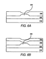
- Figs. 6A - 6B collectively illustrate a method of fabricating the fifth embodiment of the electron emitter 300 shown in Fig. 3A.
- the fabrication step shown in Fig. 4A is substantially similar to that in this fifth embodiment and thus need not be shown in detail.
- Fig. 6A departs from Fig. 4B in that instead of forming an insulator that is relatively bumped at the top, an hourglass-shaped insulator 340 is formed. Any given relatively thin region of the insulator 340 may be adjacent to any given protrusion 330.
- the top conductive layer 350 may be formed above the insulator 340 to fabricate the fifth and sixth embodiments of the FEMIS electron emitter 300, as shown in Fig. 6B. Note that the top conductive layer 350 preferably conforms to the shape of the insulator 340.
Abstract
In an electron emitter (100, 200, 300) based on Metal-Insulator-Semiconductor or
Metal-Insulator-Metal emitters, field emission structures are enclosed within the emitter
structure. The electron emitter may include a conductive substrate (110, 210, 310) and an
electron supply layer (120, 220, 320) formed on the conductive substrate (110, 210, 310).
The electron supply layer (120, 220, 320), for example undoped polysilicon, has
protrusions (130, 230, 330) formed on its surface. The sharpness and density of
protrusions (130, 230, 330) may be controlled. Above the electron supply layer (120,
220, 320) and the protrusions, an insulator (140, 240, 340) may be formed thereby
enclosing the protrusions (130, 230, 330). A top conductive layer (150, 250, 350) may be
formed above the insulator (140, 240, 340). The enclosed protrusions (130, 230, 330) are
relatively insensitive to vacuum contamination. The thinness of the insulator (140, 240,
340) allows high intensity electric fields at the protrusions (130, 230, 330) to be generated
with low applied voltage. Field-enhanced injection of electrons into the insulator (140,
240, 340) and thence through the top conductive layer (150, 250, 350) results.
Furthermore, electron beam dispersion and divergence are minimized.
Description
- This invention relates generally to field enhanced Metal-Insulator-Semiconductor (MIS) or Metal-Insulator-Metal (MIM) electron emitter devices, hereinafter collectively referred to as FEMIS and to methods for fabricating such devices.
- Electron emission technology exists in many forms today. For example, cathode ray tubes (CRT) are prevalent in many devices such as TVs and computer monitors. Electron emission plays a critical role in devices such as x-ray machines and electron microscopes. In addition, microscopic cold cathodes can be employed in electron-beam lithography used, for example, in making integrated circuits, in information storage devices such as those described in Gibson et al, U.S. Patent 5,557,596, in microwave sources, in electron amplifiers, and in flat panel displays. Actual requirements for electron emission vary according to application. In general, electron beams need to deliver sufficient current, be as efficient as possible, operate at application-specific voltages, be focusable, be reliable at the required power densities, and be stable both spatially and temporally at a reasonable vacuum for any given application. Portable devices, for example, demand low power consumption.
- Metal-Insulator-Semiconductor (MIS) and Metal-Insulator-Metal (MIM) electron emitter structures are described in Iwasaki, et al, U.S. Patent 6,066,922. In such structures with the application of a potential between the electron supply layer and the thin metal top electrode, electrons are 1) injected into the insulator layer from the electron supply layer (metal or semiconductor), 2) accelerated in the insulator layer, 3) injected into the thin metal top electrode, and 4) emitted from the surface of the thin metal top electrode. Depending upon the magnitude of the potential between the electron supply and thin metal top electrode layers, such emitted electrons can possess kinetic energy substantially higher than thermal energy at the surface of the thin metal film. Hence, these emitters may also be called ballistic electron emitters.
- Shortcomings of MIS or MIM devices include relatively low emission current densities (typically about 1 to 10 mA/cm2) and poor efficiencies (defined as the ratio of emitted current to shunt current between the electron supply layer and the thin metal electrode) (typically approximately 0.1 %).
- Electrons may also be emitted from conducting or semiconducting solids into a vacuum through an application of an electric field at the surface of the solid. This type of electron emitter is commonly referred to as a field emitter. Emitted electrons from field emitters possess no kinetic energy at the surface of the solid. The process for making tip-shaped electron field emitters, hereinafter referred to as Spindt emitters, is described in C. A. Spindt, et al, "Physical Properties of Thin-Film Field Emission Cathodes with Molybdenum Cones", Journal of Applied Physics, vol. 47, No. 12, December 1976, pp. 5248-5263. For a Spindt emitter, the electron-emitting surface is shaped into a tip in order to induce a stronger electric field at the tip surface for a given potential between the tip surface and an anode; the sharper the tip, the lower the potential necessary to extract electrons from the emitter.
- The shortcomings of Spindt emitters include requiring a relatively hard vacuum (pressure < 10-6 Torr, preferably < 10-8 Torr) to provide both spatial and temporal stability as well as reliability. Furthermore, the angle of electron emission is relatively wide with Spindt emitters making emitted electron beams relatively more difficult to focus to spot sizes required for electron-beam lithography or information storage applications. Operational bias voltages for simple Spindt tips are relatively high, ranging up to 1000 volts for a tip-to-anode spacing of 1 millimeter.
- In other words, combining high current density, stability, and reliability in one device has been difficult, if not impossible, with previous designs of electron emitters.
- In one aspect, an embodiment of a FEMIS electron emitter may include an electron supply structure. The electron supply structure is such that at least one protrusion, preferably a plurality of protrusions, may be formed on a top side of the electron supply structure. The electron supply structure may be formed from a conductive substrate and optionally an electron supply layer formed above the conductive substrate. The electron emitter may also include an insulator formed above the electron supply structure and protrusion(s). In this manner, any given protrusion becomes internal to the electron emitter structure. The electron emitter may further include a top conductive layer formed above the insulator.
- The FEMIS electron emitter may be such that a portion of the insulator above any given protrusion is thinner than a portion of the insulator that is above the relatively flat region of the electron supply structure. Additionally the insulator may be shaped to curve inward on both lower and upper sides near any given protrusion, i.e., the insulator may be hourglass-shaped locally. The insulator can also be substantially conformal to the electron supply layer, i.e., have the shape of the surface of the electron supply layer including protrusions prior to the formation of the insulator.
- In another aspect, an embodiment of a method of forming an FEMIS electron emitter may include forming an electron supply structure. The electron supply structure is such that at least one protrusion, preferably a plurality of protrusions, may be formed on a top side of the electron supply structure. The electron supply structure may be formed from a conductive substrate and optionally from an electron supply layer formed above the conductive layer substrate. The method may also include forming an insulator above the electron supply structure and protrusion(s). In this manner, any given protrusion becomes internal to the electron emitter structure. The method may further include forming a top conductive layer above the insulator.
- Certain embodiments of the present invention may be capable of achieving certain aspects. For example, because any given protrusion is internal to the emitter structure, it is not exposed to vacuum. Thus, the emitter is relatively insensitive to the contaminants that may exist in the vacuum, a situation that helps to prolong the life and efficiency of the emitter as well as to promote the spatial and temporal stability of the electron beam emitted. Consequently, vacuum requirements can be substantially relaxed.
- Moreover, the shape of any given protrusion coupled with a relatively thin insulator gives rise to an enhanced electric field at that protrusion when a voltage is applied between the conductive substrate and the top conductive layer. Relatively low operational voltages are therefore possible with FEMIS electron emitters. The electric field away from any given protrusion is relatively low thereby improving the reliability of the entire emitter structure. Current densities and efficiencies from FEMIS electron emitters can be relatively high. The electron beam from a FEMIS emitter is also relatively easy to focus.
- Features of a number of preferred embodiments of the present invention will become apparent to those skilled in the art from the following description with reference to the drawings, in which:
- Figs. 1A and 1B illustrate exemplary cross sections of first and second embodiments of an electron emitter according to an aspect of the present invention;
- Figs. 2A and 2B illustrate exemplary cross sections of third and fourth embodiments of an electron emitter according to an aspect of the present invention;
- Figs. 3A and 3B illustrate exemplary cross sections of fifth and sixth embodiments of an electron emitter according to an aspect of the present invention;
- Figs. 4A - 4C collectively illustrate an exemplary method of fabricating the first embodiment of the electron emitter shown in Fig. 1A;
- Figs. 5A - 5B collectively illustrate an exemplary method of fabricating the third embodiment of the electron emitter shown in Fig. 2A; and
- Figs. 6A - 6B collectively illustrate an exemplary method of fabricating the fifth embodiment of an electron emitter shown in Fig. 3A.
-
- For simplicity and illustrative purposes, a number of preferred embodiments of the present invention are described. However, one of ordinary skill in the art would readily recognize that the same principles are equally applicable to many types of electron emitters.
- Figs. 1A and 1B illustrate cross sections of first and second embodiments of an exemplary
FEMIS electron emitter 100 according to an aspect of the present invention. As shown, theelectron emitter 100 may include aconductive substrate 110. Theconductive substrate 110 may be formed from metal (aluminum, tungsten, titanium, copper, gold, tantalum, platinum, iridium, palladium, rhodium, chromium, magnesium, scandium, yttrium, vanadium, zirconium, niobium, molybdenum, silicon, beryllium, hafnium, silver, and osmium and any alloys, and multilayered films thereof); doped polysilicon; doped silicon; graphite; metal-coated glass, ceramic, or plastic; indium-tin-oxide (ITO) coated glass, ceramic, or plastic; and the like. The metal or ITO coatings may be patterned or unpattemed. The top surface of the conductive substrate may be planarized using generally accepted methods such as chemical-mechanical polishing (CMP). - Above the
conductive substrate 110, theelectron emitter 100 may also include anelectron supply layer 120 as shown in Fig. 1A. As shown in Fig. 1B, theelectron supply layer 120 is not necessary to practice the invention. Aprotrusion 130 may be formed on a top side of the electron supply layer 120 (see Fig. 1A) or on a top side of the conductive substrate 110 (see Fig. 1B). There may be many of theseprotrusions 130 included in theelectron emitter 100. The sharpness of any givenprotrusion 130 may be controlled in the fabrication process. As a result, the current output perprotrusion 130 may be obtained at relatively lower voltages according to Fowler-Nordheim emission statistics. - The density of the
protrusions 130 may also be controlled. For example, densities of several hundredprotrusions 130 per square micrometer can be obtained. Consequently the total emission current can be controlled. Since any givenprotrusion 130 may be capable of delivering a given current in the limit, higher current may be delivered by increasing the number ofprotrusions 130 per emission area. Since the current can be related to voltage applied between theconductive substrate 110 and a topconductive layer 150 through the Fowler-Nordheim equation, control voltages, hence power, can be adjusted downward depending upon application. - The
electron supply layer 120, including the protrusion(s) 130 of theelectron emitter 100, may be formed from a semiconductor, such as polysilicon, that may or may not be doped. In a preferred embodiment, the polysilicon may be undoped. If n-type doping is preferable, the level of doping along a depth of theelectron supply layer 120 may be varied to tailor electron transport. In addition, the doping may be confined to given areas through the use of masks. - The formation of the protrusion(s) 130 may be accomplished through the growth of hemispherical grain (HSG) polysilicon as part of the process in forming the polysilicon comprising the
electron supply layer 120 or theconductive substrate 110. Alternatively, the growth of protrusion(s) 130 may be effected by seeding the growth of HSG polysilicon in subsequent processes. HSG polysilicon is described in M. Yoshimaru, et al, "Rugged surface poly-Si electrode and low temperature deposited Si3N4 for 64 Mbit and beyond STC DRAM cell", Tech. Digest, 1990 International Electron Devices Meeting, San Francisco, December 9-12, 1990, paper 27.4, pp. 659-662. - The
electron emitter 100 may further include aninsulator 140 formed above theelectron supply layer 120 or theconductive substrate 110 including the protrusion(s) 130. In this manner, the protrusion(s) 130 becomes internal to the structure of theelectron emitter 100, and the protrusion(s) 130 is not exposed to vacuum. Theinsulator 140 may be formed from materials such as the oxides, nitrides, and oxynitrides of silicon, aluminum, titanium, tantalum, tungsten, hafnium, zirconium, vanadium, niobium, molybdenum, chromium, yttrium, scandium, nickel, cobalt, beryllium, magnesium, and combinations thereof. The insulator may also be formed from diamond-like carbon. However, one of ordinary skill will realize that the list of materials is not exhaustive. Indeed, theinsulator 140 may be formed by oxidizing a top portion of theelectron supply layer 120. - The
insulator 140 may be formed such that theinsulator 120 is substantially conformal with theelectron supply layer 120 or theconductive substrate 110 including protrusion(s) 130. The lower bound on the thickness of theinsulator 140 may be largely determined by the potential between theelectron supply layer 120 and the topconductive layer 150 that is sufficient to overcome the work function of the topconductive layer 150, which is typically 4 to 6 electron volts (eV). Breakdown voltage of theinsulator 140 at any given thickness and the work function of the topconductive layer 150 therefore dictate the lower bound on the thickness of theinsulator 140. The upper bound on the thickness of theinsulator 140 may be determined by the potential necessary to cause electron transport in theinsulator 140. The thicker theinsulator 140 is; the higher the required potential. - The thinness of the
insulator 140 near any givenprotrusion 130 and the shape of any givenprotrusion 130 allows a relatively large electric field to be generated at relatively low applied bias voltages between theconductive substrate 110 and the topconductive layer 150. For the example of an FEMIS emitter formed of undoped polysilicon and an insulator thickness of 25 nm, only about a 6 volt bias needs to be applied to generate a sufficient electric field to give rise to electron emission by overcoming the work function of the topconductive layer 150. For typical Spindt emitters without extraction electrodes and a tip-to-anode spacing of 1 mm, the applied potential would be approximately 1,000 Volts. - Additionally, the
electron emitter 100 may include the topconductive layer 150 formed above theinsulator 140. The topconductive layer 150 may be formed from metal (aluminum, tungsten, titanium, molybdenum titanium, copper, gold, silver, tantalum, platinum, iridium, palladium, rhodium, chromium, magnesium, scandium, yttrium, vanadium, zirconium, niobium, molybdenum, hafnium, silver, and osmium and any alloys or multilayered films), doped polysilicon, graphite, etc. or combinations of metal and non-metal, e.g., conductive carbon, films. When exposed to air the outer surface of the topconductive layer 150 is preferred to not oxidize to an insulating native oxide. - To operate the
FEMIS electron emitter 100, a bias voltage is applied between theconductive substrate 110 and the topconductive layer 150. During operation, electrons transported through the conductive substrate 110 (and the electron supply layer 120) tunnel through theinsulator 140 near any givenprotrusion 130 and are emitted from the topconductive layer 150. - Figs. 2A and 2B illustrate cross sections of third and fourth embodiments of an exemplary
FEMIS electron emitter 200 according to an aspect of the present invention. The third and fourth embodiments may include many of the same features described herein with respect to first and second embodiments, respectively, of Figs. 1A and 1B. For example, theelectron emitter 200 may include a conductive substrate 210 (with at least oneprotrusion 230, see Fig. 2A), optionally anelectron supply layer 220 with at least one protrusion 230 (see Fig. 2B), aninsulator 240, and a topconductive layer 250. Only those elements distinguishable between the embodiments are described. - Regarding the
electron emitter 200, theinsulator 240 may be formed such that theinsulator 240 near any givenprotrusion 230 is relatively thinner than theinsulator 240 on regions of theelectron supply layer 220 that are substantially flat. For example, the thickness of theinsulator 240 near theprotrusion 130 may be between 5 - 300 nanometers (nm), but may be 30 - 325 nm thick in the substantially flat region assuming that the protrusion(s) 230 protrudes 25 nm above the substantially flat regions of theelectron supply layer 220. In this third and fourth embodiments, the outer surface of theinsulator 240 is relatively flat. Focusing of the emitted electron beam may be improved with such structure through control of electron beam divergence. The same arguments with respect to limits on the thickness of theinsulator 240 above the protrusion(s) 230 still pertain. - Figs. 3A and 3B illustrate cross sections of fifth and sixth embodiments of an exemplary
FEMIS electron emitter 300 according to another aspect of the present invention. The fifth and sixth embodiments may include many of the same features described herein with respect to first and second embodiments, respectively, of Figs. 1A and 1B. For example, theelectron emitter 300 may include a conductive substrate 310 (at least oneprotrusion 130, see Fig. 3A), optionally anelectron supply layer 320 with at least one protrusion 330 (see Fig. 3B), aninsulator 340, and a topconductive layer 350. Only those elements distinguishable amongst the embodiments are described. - Regarding the
electron emitter 300, the shape of theinsulator 340 is such that a horizontal hourglass shape is formed near any givenprotrusion 330. Focusing of the emitted electron beam may be further improved with such structure. The same arguments with respect to limits on the thickness of theinsulator 340 above the protrusion(s) 330 still pertain. - Figs. 4A - 4C collectively illustrate a method of fabricating the first embodiment of the
electron emitter 100 shown in Fig. 1A. As shown in Fig. 4A, theconductive substrate 110 may be formed.Protrusions 130 may be formed at this point as part of forming the conductive substrate 110 (not shown). Optionally theelectron supply layer 120 may be formed above theconductive substrate 110 and the protrusion(s) 130 may be formed as part of the forming theelectron supply layer 120. Note that the top of theconductive substrate 110 may be planarized using commonly known techniques such as CMP prior to forming theelectron supply layer 120. - If polysilicon is used to form the
electron supply layer 120, the polysilicon, including the protrusion(s) 130, may be grown on theconductive substrate 110 by low pressure chemical-vapor-deposition (LPCVD). A preferred temperature when performing LPCVD is substantially between 550 C° and 620 C°. The preferred thickness of the polysilicon may range substantially between 0.05 µm and 1 µm. The polysilicon may be grown through other deposition processes such as plasma-enhanced chemical-vapor-deposition (PECVD), other CVD variations, or physical vapor deposition (PVD) techniques that include sputter deposition and evaporation. - The
electron supply layer 120, including the protrusion(s) 130, may be doped or undoped. As an option, theelectron supply layer 120, such as the polysilicon, may be doped through incorporation of an n-type dopant such as phosphorous, arsenic or antimony during deposition of the polysilicon. One of ordinary skill will realize that other types of dopants are possible. The dopant concentration may be modified over time so that different depth levels of theelectron supply layer 120 have varying dopant levels. Alternatively, ion implantation and subsequent annealing may also be used for either uniform or graded dopant incorporation after theelectron supply layer 120 has been formed. - After the electron supply layer 120 (or the conductive substrate 110) is formed, the
insulator 140 may be formed above theelectron supply layer 120 as shown in Fig. 4B. When theinsulator 140 is formed, the electron supply layer 120 (or the conductive substrate 110) and the protrusion(s) 130 become substantially conformally covered, i.e., any givenprotrusion 130 becomes internal to the emitter structure. Any givenprotrusion 130 is consequently not exposed to vacuum and therefore becomes relatively insensitive to the vagaries of the vacuum environment during operation of the electron emitter. As a result, vacuum requirements are relaxed. - Indeed, the
insulator 140 may be formed through oxidizing the polysilicon, for example, by rapid oxidation in a dry oxygen atmosphere at a temperature substantially ranging between 800 C° and 1000 C° and time substantially between 5 and 60 minutes. Other methods of oxidation include but are not limited to plasma oxidation, wet thermal oxidation, and electrochemical oxidation. - To complete the process, the top
conductive layer 150 may be formed above theinsulator 140 to fabricate theFEMIS electron emitter 100, as shown in Fig. 4C. - Fig. 5A - 5B collectively illustrate a method of fabricating the third embodiment of the
electron emitter 200 shown in Figs. 2A. The fabrication step shown in Fig. 4A is substantially similar to that for this third embodiment and thus need not be described in detail. Fig. 5A departs from Fig. 4B in that instead of the forming an insulator that is relatively bumped at the top, a substantiallyflat insulator 240 is formed. The relatively thin region of theinsulator 240 is near any givenprotrusion 230. - Subsequent to forming the
insulator 240, the topconductive layer 250 may be formed above theinsulator 240 to fabricate the third and fourth embodiments of theFEMIS electron emitter 200, as shown in Fig. 5B. Note that the topconductive layer 250 is substantially flat. - Figs. 6A - 6B collectively illustrate a method of fabricating the fifth embodiment of the
electron emitter 300 shown in Fig. 3A. The fabrication step shown in Fig. 4A is substantially similar to that in this fifth embodiment and thus need not be shown in detail. Fig. 6A departs from Fig. 4B in that instead of forming an insulator that is relatively bumped at the top, an hourglass-shapedinsulator 340 is formed. Any given relatively thin region of theinsulator 340 may be adjacent to any givenprotrusion 330. - Subsequent to forming the
insulator 340, the topconductive layer 350 may be formed above theinsulator 340 to fabricate the fifth and sixth embodiments of theFEMIS electron emitter 300, as shown in Fig. 6B. Note that the topconductive layer 350 preferably conforms to the shape of theinsulator 340. - While the invention has been described with reference to the exemplary embodiments thereof, those skilled in the art will not be able to make various modifications to the described embodiments of the invention without departing from the true scope of the invention. The terms and descriptions used herein are set forth by way of illustration only and are not meant as limitations. In particular, although the method of the present invention has been described by examples, the steps of the method may be performed in a different order than illustrated or simultaneously. Those skilled in the art will recognize that these and other variations are possible within the scope of the invention as defined in the following claims and their equivalents.
Claims (10)
- A field-enhanced MIS/MIM electron emitter device (100, 200, 300), comprising:an electron supply structure (110, 120, 210, 220, 310, 320);at least one protrusion (130, 230, 330) formed on a top surface of said electron supply structure (110, 120, 210, 220, 310, 320);an insulator (140, 240, 340) formed above said electron supply structure and said at least one protrusion (130, 230, 330); anda top conductive (150, 250, 350) layer formed on said insulator.
- A device as claimed in claim 1, wherein said electron supply structure comprises a conductive substrate (110, 210, 310); or a conductive substrate (110, 210, 310) and an electron supply layer (120, 220, 320).
- A device as claimed in claim 2, wherein said electron supply layer is formed from either a doped or an undoped semiconductor.
- A device as claimed in any preceding claim, wherein said insulator (140) is substantially conformal to said electron supply structure (110, 120) including said at least one protrusion (130).
- A device as claimed in any preceding claim, wherein said insulator (240, 340) is relatively thinner near said at least one protrusion (230, 340) compared to flat regions of said electron supply structure (210, 220, 310, 320).
- A device as claimed in any preceding claim, wherein said insulator (240) has a substantially flat top surface or said insulator (340) has an hourglass shape local to said at least one protrusion (230, 330).
- A method of fabricating a field-enhanced MIS/MIM electron emitter device (100, 200, 300), comprising:forming an electron supply structure (110, 120, 210, 220, 310, 320);forming at least one protrusion (130, 230, 330) on a top surface of said electron supply structure (110, 120, 210, 220, 310, 320);forming an insulator (140, 240, 340) above said electron supply structure and said at least one protrusion (130, 230, 330); andforming a top conductive (150, 250, 350) layer on said insulator.
- A method as claimed in claim 7, wherein said step of forming said electron supply structure (110, 120, 210, 220, 310, 320) includes:forming a conductive substrate (110, 210, 310); or a conductive substrate (110, 210, 310) and an electron supply layer (120, 220, 320).
- A method as claimed in claim 7 or 8, wherein said step of forming said insulator includes:forming said insulator such that said insulator (140) is substantially conformal to said electron supply structure (110, 120) including said at least one protrusion (130).
- A method as claimed in any of claims 7 to 9, wherein said step of forming said insulator (240, 340) includes:forming said insulator (240, 340) such that said insulator (240, 340) is relatively thinner near said at least one protrusion (230, 330) compared to a flat region of said electron supply layer (210, 220, 310, 320).
Applications Claiming Priority (2)
| Application Number | Priority Date | Filing Date | Title |
|---|---|---|---|
| US975296 | 2001-10-12 | ||
| US09/975,296 US6822380B2 (en) | 2001-10-12 | 2001-10-12 | Field-enhanced MIS/MIM electron emitters |
Publications (1)
| Publication Number | Publication Date |
|---|---|
| EP1302964A1 true EP1302964A1 (en) | 2003-04-16 |
Family
ID=25522876
Family Applications (1)
| Application Number | Title | Priority Date | Filing Date |
|---|---|---|---|
| EP02257067A Withdrawn EP1302964A1 (en) | 2001-10-12 | 2002-10-11 | Field-enhanced MIS/MIM electron emitters |
Country Status (4)
| Country | Link |
|---|---|
| US (1) | US6822380B2 (en) |
| EP (1) | EP1302964A1 (en) |
| JP (1) | JP2003162956A (en) |
| CN (1) | CN1412804A (en) |
Cited By (2)
| Publication number | Priority date | Publication date | Assignee | Title |
|---|---|---|---|---|
| US6833868B1 (en) | 1998-12-10 | 2004-12-21 | Imec Vzw | Method and device for determining corrected color aspects of a pixel in an imaging device |
| EP2390896A1 (en) * | 2010-05-28 | 2011-11-30 | Canon Kabushiki Kaisha | Electron gun, lithography apparatus, method of manufacturing article, and electron beam apparatus |
Families Citing this family (11)
| Publication number | Priority date | Publication date | Assignee | Title |
|---|---|---|---|---|
| TWI234124B (en) * | 2003-06-30 | 2005-06-11 | Ritdisplay Corp | Display panel, electrode panel and electrode substrate thereof |
| TW586336B (en) * | 2003-06-30 | 2004-05-01 | Ritdisplay Corp | Electrode substrate of flat panel display |
| TW591579B (en) * | 2003-06-30 | 2004-06-11 | Ritdisplay Corp | Display panel, electrode panel and electrode substrate thereof |
| JP5528736B2 (en) * | 2009-07-27 | 2014-06-25 | 株式会社デンソー | Thermoelectric generator |
| JP5238795B2 (en) * | 2010-11-19 | 2013-07-17 | シャープ株式会社 | Electron emitting device and driving method thereof |
| CN104795300B (en) * | 2014-01-20 | 2017-01-18 | 清华大学 | Electron emission source and manufacturing method thereof |
| CN104795297B (en) * | 2014-01-20 | 2017-04-05 | 清华大学 | Electron emitting device and electron emission display device |
| CN104795298B (en) * | 2014-01-20 | 2017-02-22 | 清华大学 | Electron emission device and display |
| CN104795293B (en) * | 2014-01-20 | 2017-05-10 | 清华大学 | Electron emission source |
| CN104795292B (en) * | 2014-01-20 | 2017-01-18 | 清华大学 | Electron emission device, manufacturing method thereof and display |
| CN104795291B (en) * | 2014-01-20 | 2017-01-18 | 清华大学 | Electron emission device, manufacturing method thereof and display |
Citations (7)
| Publication number | Priority date | Publication date | Assignee | Title |
|---|---|---|---|---|
| JPS62272421A (en) * | 1986-05-20 | 1987-11-26 | Canon Inc | Electron emitting element |
| EP0367195A2 (en) * | 1988-10-31 | 1990-05-09 | Matsushita Electric Industrial Co., Ltd. | Mim cold-cathode electron emission elements and methods of manufacture thereof |
| EP0878819A2 (en) * | 1997-05-15 | 1998-11-18 | Pioneer Electronic Corporation | Electron emission device and display device using the same |
| US6037606A (en) * | 1997-11-10 | 2000-03-14 | Nec Corporation | Construction of and method of manufacturing an MIM or MIS electron source |
| EP1056110A1 (en) * | 1998-02-09 | 2000-11-29 | Matsushita Electric Industrial Co., Ltd. | Electron emitting device, method of producing the same, and method of driving the same; and image display comprising the electron emitting device and method of producing the same |
| JP2001110300A (en) * | 1999-10-08 | 2001-04-20 | Fujitsu Ltd | Field emission cathode |
| EP1117118A1 (en) * | 2000-01-13 | 2001-07-18 | Pioneer Corporation | Electron-emitting device and method of manufacturing the same and display apparatus using the same |
Family Cites Families (9)
| Publication number | Priority date | Publication date | Assignee | Title |
|---|---|---|---|---|
| US3581151A (en) * | 1968-09-16 | 1971-05-25 | Bell Telephone Labor Inc | Cold cathode structure comprising semiconductor whisker elements |
| US3717790A (en) * | 1971-06-24 | 1973-02-20 | Bell Telephone Labor Inc | Ion implanted silicon diode array targets for electron beam camera tubes |
| US5619092A (en) | 1993-02-01 | 1997-04-08 | Motorola | Enhanced electron emitter |
| US5599749A (en) | 1994-10-21 | 1997-02-04 | Yamaha Corporation | Manufacture of micro electron emitter |
| US5557596A (en) | 1995-03-20 | 1996-09-17 | Gibson; Gary | Ultra-high density storage device |
| US6204595B1 (en) | 1995-07-10 | 2001-03-20 | The Regents Of The University Of California | Amorphous-diamond electron emitter |
| JP3526673B2 (en) | 1995-10-09 | 2004-05-17 | 富士通株式会社 | Electron-emitting device, electron-emitting device array, cathode plate, their manufacturing method, and flat display device |
| US6187603B1 (en) | 1996-06-07 | 2001-02-13 | Candescent Technologies Corporation | Fabrication of gated electron-emitting devices utilizing distributed particles to define gate openings, typically in combination with lift-off of excess emitter material |
| US5908699A (en) | 1996-10-11 | 1999-06-01 | Skion Corporation | Cold cathode electron emitter and display structure |
-
2001
- 2001-10-12 US US09/975,296 patent/US6822380B2/en not_active Expired - Fee Related
-
2002
- 2002-10-04 JP JP2002292820A patent/JP2003162956A/en active Pending
- 2002-10-11 CN CN02143588A patent/CN1412804A/en active Pending
- 2002-10-11 EP EP02257067A patent/EP1302964A1/en not_active Withdrawn
Patent Citations (7)
| Publication number | Priority date | Publication date | Assignee | Title |
|---|---|---|---|---|
| JPS62272421A (en) * | 1986-05-20 | 1987-11-26 | Canon Inc | Electron emitting element |
| EP0367195A2 (en) * | 1988-10-31 | 1990-05-09 | Matsushita Electric Industrial Co., Ltd. | Mim cold-cathode electron emission elements and methods of manufacture thereof |
| EP0878819A2 (en) * | 1997-05-15 | 1998-11-18 | Pioneer Electronic Corporation | Electron emission device and display device using the same |
| US6037606A (en) * | 1997-11-10 | 2000-03-14 | Nec Corporation | Construction of and method of manufacturing an MIM or MIS electron source |
| EP1056110A1 (en) * | 1998-02-09 | 2000-11-29 | Matsushita Electric Industrial Co., Ltd. | Electron emitting device, method of producing the same, and method of driving the same; and image display comprising the electron emitting device and method of producing the same |
| JP2001110300A (en) * | 1999-10-08 | 2001-04-20 | Fujitsu Ltd | Field emission cathode |
| EP1117118A1 (en) * | 2000-01-13 | 2001-07-18 | Pioneer Corporation | Electron-emitting device and method of manufacturing the same and display apparatus using the same |
Non-Patent Citations (2)
| Title |
|---|
| PATENT ABSTRACTS OF JAPAN vol. 012, no. 158 (E - 608) 13 May 1988 (1988-05-13) * |
| PATENT ABSTRACTS OF JAPAN vol. 2000, no. 21 3 August 2001 (2001-08-03) * |
Cited By (2)
| Publication number | Priority date | Publication date | Assignee | Title |
|---|---|---|---|---|
| US6833868B1 (en) | 1998-12-10 | 2004-12-21 | Imec Vzw | Method and device for determining corrected color aspects of a pixel in an imaging device |
| EP2390896A1 (en) * | 2010-05-28 | 2011-11-30 | Canon Kabushiki Kaisha | Electron gun, lithography apparatus, method of manufacturing article, and electron beam apparatus |
Also Published As
| Publication number | Publication date |
|---|---|
| CN1412804A (en) | 2003-04-23 |
| US20030071555A1 (en) | 2003-04-17 |
| US6822380B2 (en) | 2004-11-23 |
| JP2003162956A (en) | 2003-06-06 |
Similar Documents
| Publication | Publication Date | Title |
|---|---|---|
| US6629869B1 (en) | Method of making flat panel displays having diamond thin film cathode | |
| US5341063A (en) | Field emitter with diamond emission tips | |
| US6075315A (en) | Field-emission cold cathode having improved insulating characteristic and manufacturing method of the same | |
| US6770497B2 (en) | Field emission emitter | |
| US5702281A (en) | Fabrication of two-part emitter for gated field emission device | |
| US5717279A (en) | Field emission cathode with resistive gate areas and electron gun using same | |
| US6822380B2 (en) | Field-enhanced MIS/MIM electron emitters | |
| EP1384244B1 (en) | Tunneling emitter | |
| KR100449071B1 (en) | Cathode for field emission device | |
| US7057333B1 (en) | Method and device for extraction of electrons in a vacuum and emission cathodes for said device | |
| US5804909A (en) | Edge emission field emission device | |
| JP2809078B2 (en) | Field emission cold cathode and method of manufacturing the same | |
| US6902458B2 (en) | Silicon-based dielectric tunneling emitter | |
| JP2002083555A (en) | Self-aligned electron souce device | |
| JP2002520770A (en) | Field emission element | |
| US6960876B2 (en) | Electron emission devices | |
| WO2003073480A2 (en) | Emission layer formed by rapid thermal formation process | |
| US6144145A (en) | High performance field emitter and method of producing the same | |
| JP3502883B2 (en) | Cold electron-emitting device and method of manufacturing the same | |
| Chubun et al. | Fabrication and characterization of singly addressable arrays of polysilicon field-emission cathodes | |
| JP3079086B2 (en) | Method for manufacturing field emission electron source | |
| JP2002539580A (en) | Field emission device and method of use | |
| Han et al. | Lateral silicon field-emission devices using electron beam lithography | |
| WO1999063568A1 (en) | Gate-and emitter array on fiber electron field emission structure | |
| JP2000090811A (en) | Cold electron emitting element and manufacture thereof |
Legal Events
| Date | Code | Title | Description |
|---|---|---|---|
| PUAI | Public reference made under article 153(3) epc to a published international application that has entered the european phase |
Free format text: ORIGINAL CODE: 0009012 |
|
| AK | Designated contracting states |
Designated state(s): AT BE BG CH CY CZ DE DK EE ES FI FR GB GR IE IT LI LU MC NL PT SE SK TR |
|
| AX | Request for extension of the european patent |
Extension state: AL LT LV MK RO SI |
|
| 17P | Request for examination filed |
Effective date: 20031006 |
|
| AKX | Designation fees paid |
Designated state(s): DE FR |
|
| RBV | Designated contracting states (corrected) |
Designated state(s): DE GB |
|
| STAA | Information on the status of an ep patent application or granted ep patent |
Free format text: STATUS: THE APPLICATION HAS BEEN WITHDRAWN |
|
| 18W | Application withdrawn |
Effective date: 20060123 |