CN1412804A - Field enhancement metal insulator-semiconductor/metal insulator-metal electronic emitter - Google Patents
Field enhancement metal insulator-semiconductor/metal insulator-metal electronic emitter Download PDFInfo
- Publication number
- CN1412804A CN1412804A CN02143588A CN02143588A CN1412804A CN 1412804 A CN1412804 A CN 1412804A CN 02143588 A CN02143588 A CN 02143588A CN 02143588 A CN02143588 A CN 02143588A CN 1412804 A CN1412804 A CN 1412804A
- Authority
- CN
- China
- Prior art keywords
- insulator
- ledge
- metal
- supply structure
- electronic emitter
- Prior art date
- Legal status (The legal status is an assumption and is not a legal conclusion. Google has not performed a legal analysis and makes no representation as to the accuracy of the status listed.)
- Pending
Links
Images


Classifications
-
- H—ELECTRICITY
- H01—ELECTRIC ELEMENTS
- H01J—ELECTRIC DISCHARGE TUBES OR DISCHARGE LAMPS
- H01J1/00—Details of electrodes, of magnetic control means, of screens, or of the mounting or spacing thereof, common to two or more basic types of discharge tubes or lamps
- H01J1/02—Main electrodes
- H01J1/30—Cold cathodes, e.g. field-emissive cathode
- H01J1/312—Cold cathodes, e.g. field-emissive cathode having an electric field perpendicular to the surface, e.g. tunnel-effect cathodes of Metal-Insulator-Metal [MIM] type
-
- B—PERFORMING OPERATIONS; TRANSPORTING
- B82—NANOTECHNOLOGY
- B82Y—SPECIFIC USES OR APPLICATIONS OF NANOSTRUCTURES; MEASUREMENT OR ANALYSIS OF NANOSTRUCTURES; MANUFACTURE OR TREATMENT OF NANOSTRUCTURES
- B82Y10/00—Nanotechnology for information processing, storage or transmission, e.g. quantum computing or single electron logic
Abstract
In an electron emitter based on Metal-Insulator-Semiconductor or Metal-Insulator-Metal emitters, field emission structures are enclosed within the emitter structure. The electron emitter may include a conductive substrate and an electron supply layer formed on the conductive substrate. The electron supply layer, for example undoped polysilicon, has protrusions formed on its surface. The sharpness and density of protrusions may be controlled. Above the electron supply layer and the protrusions, an insulator may be formed thereby enclosing the protrusions. A top conductive layer may be formed above the insulator. The enclosed protrusions are relatively insensitive to vacuum contamination.
Description
Invention field
Generally speaking, the present invention relates to electronic emitter.Particularly, the present invention relates to an enhancing metal-insulator semiconductor (MIS) or metal-insulator-metal type (MIM) electronic emitter, later on they are called FEMIS together.
Background of invention
The electronics lift-off technology of today has various ways.For example, in numerous devices as TV and computer monitor, cathode ray tube (CRT) has occupied dominant role.The electronics lift-off technology plays key effect in X-ray production apparatus and electron microscope.The electron beam lithography that uses when in addition, the microcosmic cold cathode can be used to for example make the sort of information-storing device described in No. 5557596 United States Patent (USP) of integrated circuit, Gibson or the like, electron-amplifier and flat-panel monitor.The concrete condition that the actual requirement of electronics emission is depended on concrete application.But generally speaking, for all application, electron beam must provide enough big electric current, efficient is high as far as possible, with specific voltage power supply, can focus on, under the situation that guarantees power demand density, can work reliably, all highly stable on room and time under the situation that guarantees enough vacuum degree.For example, mancarried device requires power consumption very low.
The structure of metal-insulator semiconductor (MIS) and metal-insulator-metal type (MIM) electronic emitter has been described in No. 6066922 United States Patent (USP) of Iwasaki or the like.In this structure, after between bus plane and thin metal top layer electrode, having applied a voltage, electronics 1) injects insulator layer from bus plane (metal or semiconductor), 2) in insulator layer, be accelerated, 3) be injected into thin metal top layer electrode and 4) emit from thin top layer electrode surface.Along with the difference of voltage amplitude between power supply and the thin metal top layer electrode, the kinetic energy that these electronics that emit have can be higher than the energy of thermal motion on thin metallic film surface significantly.Therefore, these reflectors also can be called the ballistic electron reflector.
The shortcoming of MIS or MIM device comprises that emission is lower and (is generally 1~10mA/cm
2), efficient lower (being defined as the ratio of by-pass current between emission current and bus plane and the thin metal electrode) (being typically about 0.1%).
Also can by apply at the surface of solids electric field from the such solid of conductor or semiconductor to the vacuum emitting electrons.This electronic emitter usually is called field launcher.On the surface of solid, the electronics that emits from field launcher is without any kinetic energy.Equal on the article of delivering on the 5248th~5263 page of the applicating physical magazine of the 47th the 12nd phase of volume " physical characteristic ", to have described the technology of making pointed field launcher in December, 1976 at C.A.Spindt etc., later on this field launcher is called the Spindt reflector with thin film field-emission cathode of molybdenum cone.For the Spindt reflector, electron emitting surface is made into the shape of a point point, so that in the voltage given between pointed surface and anode, produces stronger electric field on pointed surface; This tip is sharp more, and it is low more to launch the electron institute required voltage from reflector.
The shortcoming of Spindt reflector comprises the higher vacuum degree of needs (pressure<10
-6Torr, preferably<10
-8Torr) obtains space, time stability and reliability.In addition, the electronics angle of departure of Spindt reflector is bigger, make the electron beam emit to focus on electron beam lithography or information stores use in needed point-like difficulty more.The operating bias voltage of simple Spindt tip is higher, at interval need be up to 1000 volts voltage for 1 millimeter tip-anode.
In other words, the electronic emitter before utilizing will be realized very difficulty of high current density, high stability and high reliability in a device.
The invention summary
On the one hand, the FEMIS electronic emitter embodiment can comprise an electronics supply structure.Top in this electronics supply structure can form at least one ledge, preferably a plurality of ledges.This electronics supply structure can form with a conductive substrates, also can be chosen in and form an electron supply layer on this conductive substrates.This electronic emitter can also comprise an insulator, in this electronics supply structure and formation above the ledge.In this way, all ledge all becomes the internal structure of this electronic emitter structure.This electronic emitter can further include a top conductive layer on insulator.
A part of insulator in this FEMIS electronic emitter above any given ledge is all thin than that a part of insulator above the electronics supply structure relatively flat zone.In addition, this insulator that is to say that near the low side of any given ledge with high-endly all form an aduncate curve shape part of this insulator can be a hourglass shape.This insulator also can be of similar shape with this electron supply layer basically, that is to say the shape with electron supply layer surface, and before forming insulator, it has ledge.
On the other hand, an embodiment of the method for formation FEMIS electronic emitter can form an electronics supply structure.At least one ledge can be formed on the top in this electronics supply structure, preferably forms a plurality of ledges.This electronics supply structure can form with a conductive substrates, also can select to form with the electron supply layer that forms in the conductive layer substrate.This method can also be included in insulator of top formation of this electronics supply structure and this (these) ledge.In this way, all ledge all becomes the internal structure of electronic emitter structure.This method can also be included in this and form a top conductive layer above insulator.
Certain embodiments of the present invention can realize specific function.For example, because all ledges all belong to the internal structure of emitter structures, so it can not be exposed in the vacuum.Like this, the impurity that may exist in this reflector against vacuum comparatively speaking can be inresponsive like that, does the life-span and the efficient that can prolong electronic emitter like this, improves the room and time stability of electrons emitted bundle simultaneously.Therefore, can alleviate vacuum requirements widely.
In addition, with the shape of relative all given ledges that connect than thin insulator causes applying a voltage between this conductive substrates and conductive layer top when, be enhanced at the electric field of ledge.Therefore, such FEMIS electronic emitter just might keep lower operating voltage.The electric field that comes out from any one ledge all relatively a little less than, thereby improve the stability of whole emitter structures.The current density of the electric current that the FEMIS electronic emitter comes out and efficient thereof are higher relatively.The electron beam that comes out from the FEMIS reflector also focuses on than being easier to.
The accompanying drawing summary
By following description, simultaneously with reference to the accompanying drawings, those of skill in the art can understand feature of the present invention immediately, wherein:
Figure 1A and 1B are the exemplary cross sectional view of first and second embodiment of electronic emitter in one aspect of the invention;
Fig. 2 A and 2B are the exemplary cross sectional view of the 3rd and the 4th embodiment of electronic emitter in one aspect of the invention;
Fig. 3 A and 3B are the exemplary cross sectional view of the 5th and the 6th embodiment of electronic emitter in one aspect of the invention;
Fig. 4 A~4C illustrates an illustrative methods that realizes first embodiment of electronic emitter shown in Figure 1A together;
Fig. 5 A~5B illustrates an illustrative methods that realizes the 3rd embodiment of electronic emitter shown in Fig. 2 A together;
Fig. 6 A~6B illustrates an illustrative methods that realizes the 5th embodiment of electronic emitter shown in Fig. 3 A together.
Detailed Description Of The Invention
Simultaneously in order to describe, mainly principle of the present invention is described for simple by exemplary embodiment.But those skilled in the art can understand that these principles can be used in polytype electronic emitter equally.
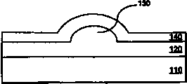
The drawn profile of first and second embodiment of exemplary FEMIS electronic emitter in one aspect of the invention of Figure 1A and 1B.As shown in the figure, this electronic emitter 100 can comprise a conductive substrates 110.This conductive substrates 110 can be used metal (aluminium, tungsten, titanium, copper, gold, tantalum, platinum, iridium, palladium, lawrencium, chromium, magnesium, scandium, yttrium, vanadium, pick, niobium, molybdenum, silicon, beryllium, hafnium, silver, osmium and any alloy, and their plural layers); Doped polycrystalline silicon; Doped silicon; Graphite; The glass of metal coat, pottery or plastics; Glass, pottery or plastics of tin indium oxide (ITO) coating or the like form.Metal here or ITO coating can be made certain shape, also can not do like this.The top surface of conductive substrates can polish with this generally accepted method of chemical-mechanical polishing (CMP).
On conductive substrates 110, electronic emitter 100 can also comprise the electron supply layer 120 shown in Figure 1A.Shown in Figure 1B, this electron supply layer 120 needn't adopt method of the present invention to make.Can form a ledge 130 at the top of this electron supply layer 120 (seeing Figure 1A) or at the top of conductive substrates 110 (seeing Figure 1B).In electronic emitter 100, can comprise many such ledges 130.Can in manufacturing process, control the acutance of any given ledge 130.As a result, learn according to the Fowler-Nordheim transmission statistic, each ledge 130 can obtain electric current with relatively low voltage.
Can also control the density of ledge 130.For example, can in each square micron, obtain a hundreds of ledge 130.Therefore can control total emission current.Because each ledge 130 all may provide a certain amount of electric current under limiting case, therefore can obtain bigger electric current by the quantity that increases ledge 130 in each emitting area.Because according to the Fowler-Nordheim formula, the voltage that applies between electric current and conductive substrates 110 and the top conductive layer 150 is relevant, therefore can reduce control voltage according to the situation of concrete application, thereby reduce power.
The formation of ledge 130 can be by particle (HSG) polysilicon of growth semi-spherical shape, and a part that forms technology as polysilicon realizes that it comprises electron supply layer 120 or conductive substrates 110.The growth of ledge 130 also can realize by plantation hsg polysilicon in the technical process afterwards.No. 27.4 paper " the low temperature depositing Si of rough surface polysilicon electrode and 64Mb and above STC DRAM unit of M.Yoshimaru or the like on the 659th~662 page of the 1990 international electronic device conferencing technology report summaries in San Francisco on the 9th~12 in December nineteen ninety
3N
4" on hsg polysilicon has been described.
At electron supply layer 120 or comprise that electronic emitter 100 can also comprise an insulator 140 on the conductive substrates 110 of ledge 130.In this way, these ledges 130 become the internal structure of electronic emitter, and these ledges can not be exposed in the vacuum.Insulator 140 can use the such metal of oxide, nitride and the nitrogen oxide of silicon, aluminium, titanium, tantalum, tungsten, hafnium, pick, vanadium, niobium, molybdenum, yttrium, scandium, cobalt, beryllium, magnesium and combination thereof to form.Insulator also can form with the same carbon of diamond.But it is not just can not adopt other material that those of ordinary skill can find to list these materials.In fact, insulator 140 can also form by oxidation is carried out at the top of electron supply layer 120.
The formation of insulator 140 can so that insulator 140 basically with electron supply layer 120 or comprise that the conductive substrates 110 of ledge 130 is of similar shape.The lower boundary of insulator 140 thickness directions can decide according to the current potential of the work function that is enough to overcome top conductive layer 150 between electron supply layer 120 and the top conductive layer 150 to a great extent, and it all is 4 to 6 electron-volts (eV) usually.The work function of any given thickness upper insulator 140 puncture voltages and top conductive layer 150 thereof has determined the lower boundary on insulator 140 thickness directions.Coboundary on insulator 140 thickness directions can be by causing the necessary current potential of electron transport to decide in the insulator 140.Insulator 140 is thick more, and required voltage is high more.
The thickness of insulator 140 is less near any given ledge 130, and the shape of any given ledge 130, all makes when the bias voltage that applies between conductive substrates 110 and the top conductive layer 150 is lower, can produce stronger electric field.For insulation thickness is 25 nanometers, and this example of FEMIS reflector that undoped polycrystalline silicon forms only needs about 6 volts bias voltage just can produce enough strong electric field, and the work function that overcomes top conductive layer 150 is come emitting electrons.For not extracting electrode, the tip is spaced apart 1 millimeter typical Spindt reflector to anode, and the voltage that applies will be about 1000 volts.
In addition, electronic emitter 100 can be included in the top conductive layer 150 that forms on the insulator 140.Top conductive layer 150 can be used metal (aluminium, tungsten, titanium, copper, gold, tantalum, platinum, iridium, palladium, lawrencium, chromium, magnesium, scandium, yttrium, vanadium, pick, niobium, molybdenum, silicon, beryllium, hafnium, silver, osmium and any alloy, and plural layers), doped polycrystalline silicon, graphite or the like or metal and nonmetal, for example the mixture of conductive carbon, film forms.Be exposed to airborne the time, the outer surface of top conductive layer 150 does not preferably carry out oxidation.
In order to allow 100 work of FEMIS electronic emitter, between conductive substrates 110 and top conductive layer 150, apply a bias voltage.In the process of work, the electronics of carrying by conductive substrates 110 (with electron supply layer 120) emits from top conductive layer 150 by near the insulator 140 any given ledge 130.
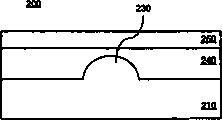
Fig. 2 A and the 2B profile in the 3rd of exemplary FEMIS electronic emitter 200 in one aspect of the invention and the 4th embodiment that drawn.Many same characteristic features when the 3rd and the 4th embodiment can comprise here respectively with reference to Figure 1A and 1B described in first and second embodiment.For example, electronic emitter 200 can comprise that a conductive substrates 210 (has a ledge 230 at least, see Fig. 2 A), can select to have at least 220, one insulators 240 of an electron supply layer and a top conductive layer 250 of a ledge 230 (seeing Fig. 2 B).Those different between these embodiments parts have only been described.
Consider electronic emitter 200, the formation of insulator 240 can be so that near the insulator 240 any given ledge 230 be all thin than the insulator on the zone of smooth basically electron supply layer 220 240.For example, the thickness of insulators 240 can be between 5~300 nanometers (nm) near the ledge 130, but can be 30~325 nanometer thickness in smooth basically zone, supposes that ledge 230 gives prominence to regional 25 nanometers of electron supply layer 220 substantially flats.In this 3rd and the 4th embodiment, the outer surface relatively flat of insulator 240.Utilize this structure,, can improve the focus level of the electron beam that emits by dispersing of controlling electron beam.Relevant being described in here for the limit of insulator 240 thickness above the ledge 230 stands good.
Fig. 3 A and 3B are the profiles in the 5th of FEMIS electronic emitter 300 exemplary in another embodiment of the invention and the 6th embodiment.The 5th and the 6th embodiment can comprise respectively first and second the described many feature of embodiment with reference to Figure 1A and 1B.For example, electronic emitter 300 can comprise a conductive substrates 310 (at least one ledge 130, see Fig. 3 A), can select to have at least the power supply supplying layer 320 (seeing Fig. 3 B) of a ledge 330, an insulator 340 and a top conductive layer 350.Those different between these embodiments compositions are only described.
Consider that electronic emitter 300, the shape of insulator 340 make near the hourglass shape of any given ledge 330 formation level.Utilize this structure can improve the focusing of electrons emitted bundle further.Suitable equally about the relevant description of the insulation thickness limit above the ledge 330 above.
Fig. 4 A~4C illustrates a kind of method that realizes electronic emitter 100 first embodiments shown in Figure 1A together.Shown in Fig. 4 A, can form conductive substrates 110.Can form ledge 130 in this, as a part (not drawing among the figure) that forms conductive substrates 110.Can be chosen in and form electron supply layer 120 above the conductive substrates 110, and form ledge 130, as a part that forms electron supply layer 120.Notice that the top of conductive substrates 110 can be carried out smooth with the such method as you know of CMP before forming electron supply layer 120.
If form electron supply layer 120 with polysilicon, polysilicon comprises ledge 130, just can grow out on conductive substrates 110 by low-pressure chemical vapor deposition (LPCVD).The optimum temperature of carrying out LPCVD is basically between 550 degrees centigrade to 620 degrees centigrade.The optimum thickness of polysilicon is basically between 0.05 micron to 1 micron.Plasma enhanced chemical vapor deposition (PECVD), other such depositing operation of other CVD method be can pass through, sputtering sedimentation and the such physical vapor deposition (PVD) technology growth polysilicon of evaporation perhaps comprised.
Formed after the electron supply layer 120 (perhaps conductive substrates 110), can on electron supply layer 120, form insulator 140, shown in Fig. 4 B.When forming insulator 140, electron supply layer 120 (perhaps conductive substrates 110) and ledge 130 are similarly covered basically, and just all ledges 130 all become the internal structure of emitter structures.Therefore all ledges 130 can not expose in a vacuum, thereby the change to vacuum environment can be so inresponsive in the course of work of electronic emitter.The result has reduced vacuum requirements.
In fact, can form insulator 140, for example, in dry oxygen, carry out quick oxidation by about 5 to 60 minutes time of cost between about 800 degrees centigrade and 1000 degrees centigrade by polysilicon is carried out oxidation.Other method for oxidation includes but not limited to plasma oxidation, damp and hot oxidation, and electrochemical oxidation.
In order to finish this process, can on insulator 140, form top conductive layer 150, to make FEMIS electronic emitter 100, shown in Fig. 4 C.
Fig. 5 A~5B is the implementation method of the 3rd embodiment of electronic emitter 200 shown in the key diagram 2A together.Making step shown in Fig. 4 A is similar to the 3rd embodiment basically, thereby do not need to describe in detail.The difference of Fig. 5 A and Fig. 4 B is that the insulator that forms is not outstanding at the top, but forms a smooth basically insulator 240.The zone that insulator 240 approaches is near ledge 230.
Formed after the insulator 240, can on insulator 240, form top conductive layer 250, to realize the 3rd and the 4th embodiment of FEMIS electronic emitter 200, shown in Fig. 5 B.Notice that top conductive layer 250 is flat basically.
Fig. 6 A~6B illustrates the method that realizes the 5th embodiment of electronic emitter 300 shown in Fig. 3 A together.Making step shown in Fig. 4 A is similar to the 5th embodiment basically, therefore do not need detailed introduction here.The difference of Fig. 6 A and Fig. 4 B is that the insulator that forms is not outstanding at the top, but forms the insulator 340 of a hourglass shape.The zone that insulator 340 approaches is near ledge 330.
Formed after the insulator 340, on insulator 340, formed top conductive layer 350, to realize the 5th and the 6th embodiment of FEMIS electronic emitter 300, shown in Fig. 6 B.Notice that the top conductive layer 350 preferably shape with insulator 340 is identical.
Though the embodiment of reference example has been described the present invention, those of skill in the art can understand that they can not carry out various changes and can not depart from the spirit and scope of the invention above-mentioned embodiment of the present invention.Here term of Cai Yonging and description is only used for describing, rather than limits.Particularly, though the description of this invention is to carry out with the form of example, can realize the step of this method according to the order that is different from explanation here.Those of skill in the art can understand that it all is possible carrying out various changes within below the claim and the spirit and scope of the invention of scope defined of their equivalents.
Claims (10)
1. a field enhancement mode MIS/MIM electronic emitter device (100,200,300) comprising:
An electronics supply structure (110,120,210,220,310,320);
At least one ledge that on the top surface of described electronics supply structure (110,120,210,220,310,320), forms (130,230,330);
An insulator (140,240,340) that forms above at described electronics supply structure and described at least one ledge (130,230,330); With
A top conductive layer (150,250,350) that on described insulator, forms.
2. the device of claim 1, electronics supply structure wherein comprises a conductive substrates (110,210,310) or a conductive substrates (110,210,310) and an electron supply layer (120,220,320).
3. the device of claim 2, electron supply layer wherein forms from one of the semiconductor that mixes and undope.
4. the device of claim 1, insulator wherein (140) is of similar shape with the described electronics supply structure (110,120) that comprises described at least one ledge (130) basically.
5. near the device of claim 1, insulator wherein (240, the 340) flat site with described electronics supply structure (210,220,310,320) described at least one ledge (230,340) is thinner relatively by comparison.
6. the device of claim 5, insulator wherein (240) has smooth basically top surface, and perhaps described insulator (340) has the shape of hourglass near described at least one ledge (230,330).
7. a kind of method of fabricating yard enhancement mode MIS/MIM electronic emitter device (100,200,300) comprising:
Form an electronics supply structure (110,120,210,220,310,320);
Top surface in described electronics supply structure (110,120,210,220,310,320) forms at least one ledge (130,230,330);
On described electronics supply structure and described at least one ledge (130,230,330), form an insulator (140,240,340); With
On described insulator, form a top conductive layer (150,250,350).
8. the method for claim 7, the described step that wherein forms described electronics supply structure (110,120,210,220,310,320) comprises:
Form a conductive substrates (110,210,310) or conductive substrates (110,210,310) and an electron supply layer (120,220,320).
9. the method for claim 7, the described step that wherein forms described insulator comprises:
Form described insulator, thereby make described insulator (140) and comprise that the described electronics supply structure (110,120) of described at least one ledge (130) is of similar shape basically.
10. the method for claim 7, the described step that wherein forms described insulator (240,340) comprises:
Form described insulator (240,340), thereby a flat site of described insulator (240,340) and described electron supply layer (210,220,310,320) is compared, near thinner relatively near described at least one ledge (230,330).
Applications Claiming Priority (2)
| Application Number | Priority Date | Filing Date | Title |
|---|---|---|---|
| US09/975,296 US6822380B2 (en) | 2001-10-12 | 2001-10-12 | Field-enhanced MIS/MIM electron emitters |
| US09/975296 | 2001-10-12 |
Publications (1)
| Publication Number | Publication Date |
|---|---|
| CN1412804A true CN1412804A (en) | 2003-04-23 |
Family
ID=25522876
Family Applications (1)
| Application Number | Title | Priority Date | Filing Date |
|---|---|---|---|
| CN02143588A Pending CN1412804A (en) | 2001-10-12 | 2002-10-11 | Field enhancement metal insulator-semiconductor/metal insulator-metal electronic emitter |
Country Status (4)
| Country | Link |
|---|---|
| US (1) | US6822380B2 (en) |
| EP (1) | EP1302964A1 (en) |
| JP (1) | JP2003162956A (en) |
| CN (1) | CN1412804A (en) |
Cited By (6)
| Publication number | Priority date | Publication date | Assignee | Title |
|---|---|---|---|---|
| CN104795293A (en) * | 2014-01-20 | 2015-07-22 | 清华大学 | Electron emission source |
| CN104795300A (en) * | 2014-01-20 | 2015-07-22 | 清华大学 | Electron emission source and manufacturing method thereof |
| CN104795297A (en) * | 2014-01-20 | 2015-07-22 | 清华大学 | Electron emission device and electron emission display |
| CN104795298A (en) * | 2014-01-20 | 2015-07-22 | 清华大学 | Electron emission device and display |
| CN104795292B (en) * | 2014-01-20 | 2017-01-18 | 清华大学 | Electron emission device, manufacturing method thereof and display |
| CN104795291B (en) * | 2014-01-20 | 2017-01-18 | 清华大学 | Electron emission device, manufacturing method thereof and display |
Families Citing this family (7)
| Publication number | Priority date | Publication date | Assignee | Title |
|---|---|---|---|---|
| EP1011262A1 (en) | 1998-12-10 | 2000-06-21 | Interuniversitair Micro-Elektronica Centrum Vzw | Method and device for determining corrected colour aspects of a pixel in an imaging device |
| TWI234124B (en) * | 2003-06-30 | 2005-06-11 | Ritdisplay Corp | Display panel, electrode panel and electrode substrate thereof |
| TW591579B (en) * | 2003-06-30 | 2004-06-11 | Ritdisplay Corp | Display panel, electrode panel and electrode substrate thereof |
| TW586336B (en) * | 2003-06-30 | 2004-05-01 | Ritdisplay Corp | Electrode substrate of flat panel display |
| JP5528736B2 (en) * | 2009-07-27 | 2014-06-25 | 株式会社デンソー | Thermoelectric generator |
| US20110294071A1 (en) * | 2010-05-28 | 2011-12-01 | Canon Kabushiki Kaisha | Electron gun, lithography apparatus, method of manufacturing article, and electron beam apparatus |
| JP5238795B2 (en) * | 2010-11-19 | 2013-07-17 | シャープ株式会社 | Electron emitting device and driving method thereof |
Family Cites Families (16)
| Publication number | Priority date | Publication date | Assignee | Title |
|---|---|---|---|---|
| US3581151A (en) * | 1968-09-16 | 1971-05-25 | Bell Telephone Labor Inc | Cold cathode structure comprising semiconductor whisker elements |
| US3717790A (en) * | 1971-06-24 | 1973-02-20 | Bell Telephone Labor Inc | Ion implanted silicon diode array targets for electron beam camera tubes |
| JPS62272421A (en) | 1986-05-20 | 1987-11-26 | Canon Inc | Electron emitting element |
| EP0367195A3 (en) | 1988-10-31 | 1991-10-02 | Matsushita Electric Industrial Co., Ltd. | Mim cold-cathode electron emission elements and methods of manufacture thereof |
| US5619092A (en) | 1993-02-01 | 1997-04-08 | Motorola | Enhanced electron emitter |
| US5599749A (en) | 1994-10-21 | 1997-02-04 | Yamaha Corporation | Manufacture of micro electron emitter |
| US5557596A (en) | 1995-03-20 | 1996-09-17 | Gibson; Gary | Ultra-high density storage device |
| US6204595B1 (en) | 1995-07-10 | 2001-03-20 | The Regents Of The University Of California | Amorphous-diamond electron emitter |
| JP3526673B2 (en) | 1995-10-09 | 2004-05-17 | 富士通株式会社 | Electron-emitting device, electron-emitting device array, cathode plate, their manufacturing method, and flat display device |
| US6187603B1 (en) | 1996-06-07 | 2001-02-13 | Candescent Technologies Corporation | Fabrication of gated electron-emitting devices utilizing distributed particles to define gate openings, typically in combination with lift-off of excess emitter material |
| US5908699A (en) | 1996-10-11 | 1999-06-01 | Skion Corporation | Cold cathode electron emitter and display structure |
| JPH10321123A (en) | 1997-05-15 | 1998-12-04 | Pioneer Electron Corp | Electron emission device and display apparatus using it |
| JP3211752B2 (en) | 1997-11-10 | 2001-09-25 | 日本電気株式会社 | Structure of MIM or MIS electron source and method of manufacturing the same |
| EP1056110B1 (en) | 1998-02-09 | 2009-12-16 | Panasonic Corporation | Electron emitting device, method of producing the same, and method of driving the same; and image display comprising the electron emitting device and method of producing the same |
| JP2001110300A (en) | 1999-10-08 | 2001-04-20 | Fujitsu Ltd | Field emission cathode |
| JP3874396B2 (en) | 2000-01-13 | 2007-01-31 | パイオニア株式会社 | ELECTRON EMITTING ELEMENT, MANUFACTURING METHOD THEREOF, AND DISPLAY DEVICE USING ELECTRON EMITTING ELEMENT |
-
2001
- 2001-10-12 US US09/975,296 patent/US6822380B2/en not_active Expired - Fee Related
-
2002
- 2002-10-04 JP JP2002292820A patent/JP2003162956A/en active Pending
- 2002-10-11 CN CN02143588A patent/CN1412804A/en active Pending
- 2002-10-11 EP EP02257067A patent/EP1302964A1/en not_active Withdrawn
Cited By (8)
| Publication number | Priority date | Publication date | Assignee | Title |
|---|---|---|---|---|
| CN104795293A (en) * | 2014-01-20 | 2015-07-22 | 清华大学 | Electron emission source |
| CN104795300A (en) * | 2014-01-20 | 2015-07-22 | 清华大学 | Electron emission source and manufacturing method thereof |
| CN104795297A (en) * | 2014-01-20 | 2015-07-22 | 清华大学 | Electron emission device and electron emission display |
| CN104795298A (en) * | 2014-01-20 | 2015-07-22 | 清华大学 | Electron emission device and display |
| CN104795292B (en) * | 2014-01-20 | 2017-01-18 | 清华大学 | Electron emission device, manufacturing method thereof and display |
| CN104795291B (en) * | 2014-01-20 | 2017-01-18 | 清华大学 | Electron emission device, manufacturing method thereof and display |
| CN104795300B (en) * | 2014-01-20 | 2017-01-18 | 清华大学 | Electron emission source and manufacturing method thereof |
| CN104795293B (en) * | 2014-01-20 | 2017-05-10 | 清华大学 | Electron emission source |
Also Published As
| Publication number | Publication date |
|---|---|
| EP1302964A1 (en) | 2003-04-16 |
| JP2003162956A (en) | 2003-06-06 |
| US6822380B2 (en) | 2004-11-23 |
| US20030071555A1 (en) | 2003-04-17 |
Similar Documents
| Publication | Publication Date | Title |
|---|---|---|
| CN1412804A (en) | Field enhancement metal insulator-semiconductor/metal insulator-metal electronic emitter | |
| US6629869B1 (en) | Method of making flat panel displays having diamond thin film cathode | |
| US6770497B2 (en) | Field emission emitter | |
| US6097139A (en) | Field electron emission materials and devices | |
| US6204595B1 (en) | Amorphous-diamond electron emitter | |
| Osikowicz et al. | Transparent low-work-function indium tin oxide electrode obtainedby molecular scale interface engineering | |
| WO1999010908A1 (en) | Electron emitting device, field emission display, and method of producing the same | |
| Kusunoki et al. | Increasing emission current from MIM cathodes by using an Ir-Pt-Au multilayer top electrode | |
| WO2001011647A1 (en) | Field emission cathodes comprised of electron emitting particles and insulating particles | |
| CN1750222A (en) | Field emission device (FED) and its method of manufacture | |
| US6891324B2 (en) | Carbon-metal nano-composite materials for field emission cathodes and devices | |
| Navitski et al. | Efficient high-current field emission from arrays of carbon nanotube columns | |
| Merkulov et al. | Field emission properties of different forms of carbon | |
| Mackie et al. | Hafnium carbide films and film-coated field emission cathodes | |
| CN1334582A (en) | Self-alignment electron source device | |
| US4038216A (en) | Material and method of making secondary-electron emitters | |
| JP2002520770A (en) | Field emission element | |
| US6870309B2 (en) | Cold emission film cathode and flat panel display with nanocrystalline carbon film emitter | |
| Jin et al. | Enhanced field emission from carbon nanotubes with a thin layer of low work function barium strontium oxide surface coating | |
| US6514112B1 (en) | Coated-wire ion bombarded graphite electron emitters | |
| US6960876B2 (en) | Electron emission devices | |
| CN1292928A (en) | M-type microwave device | |
| Ko et al. | Fabrication and simulation of a gated thin film emitter | |
| US6144145A (en) | High performance field emitter and method of producing the same | |
| US5853795A (en) | Luminant for field emission display fabricated through physical vapor deposition and method for fabricating the same |
Legal Events
| Date | Code | Title | Description |
|---|---|---|---|
| C06 | Publication | ||
| PB01 | Publication | ||
| C10 | Entry into substantive examination | ||
| SE01 | Entry into force of request for substantive examination | ||
| C02 | Deemed withdrawal of patent application after publication (patent law 2001) | ||
| WD01 | Invention patent application deemed withdrawn after publication |