EP0366373A2 - Oszillator mit Kompensierung momentaner Schwankungen des Frequenzganges - Google Patents
Oszillator mit Kompensierung momentaner Schwankungen des Frequenzganges Download PDFInfo
- Publication number
- EP0366373A2 EP0366373A2 EP89310837A EP89310837A EP0366373A2 EP 0366373 A2 EP0366373 A2 EP 0366373A2 EP 89310837 A EP89310837 A EP 89310837A EP 89310837 A EP89310837 A EP 89310837A EP 0366373 A2 EP0366373 A2 EP 0366373A2
- Authority
- EP
- European Patent Office
- Prior art keywords
- oscillator
- circuit
- transient
- frequency
- compensation circuit
- Prior art date
- Legal status (The legal status is an assumption and is not a legal conclusion. Google has not performed a legal analysis and makes no representation as to the accuracy of the status listed.)
- Withdrawn
Links
Images

Classifications
-
- H—ELECTRICITY
- H03—ELECTRONIC CIRCUITRY
- H03L—AUTOMATIC CONTROL, STARTING, SYNCHRONISATION OR STABILISATION OF GENERATORS OF ELECTRONIC OSCILLATIONS OR PULSES
- H03L1/00—Stabilisation of generator output against variations of physical values, e.g. power supply
- H03L1/02—Stabilisation of generator output against variations of physical values, e.g. power supply against variations of temperature only
-
- H—ELECTRICITY
- H03—ELECTRONIC CIRCUITRY
- H03L—AUTOMATIC CONTROL, STARTING, SYNCHRONISATION OR STABILISATION OF GENERATORS OF ELECTRONIC OSCILLATIONS OR PULSES
- H03L3/00—Starting of generators
Definitions
- This invention relates to oscillator circuits and it relates particularly, though not exclusively, to oscillator circuits which are intended to be turned on for relatively short periods of time; for example, oscillator circuits used in a radio frequency transmitter or a radio frequency receiver operating in an intermittent or sampling mode.
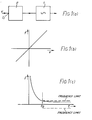
- FIG. 1(a) of the accompanying drawings shows a known oscillator circuit comprising an oscillator 1 and an associated frequency modulator 2, for example a varactor diode reactance modulator, having a control input I1 arranged to receive a control voltage V.
- Figure 1 (b) of the drawings shows how the frequency output of that oscillator circuit varies as a function of control voltage V.
- oscillations tend to grow relatively slowly giving rise to a corresponding frequency shift.
- the oscillator start frequency may not match the desired, steady state frequency.
- the frequency output of the oscillator circuit should reach a stable value as quickly as possible since the correct frequency (within acceptable error limits) may be needed in order to comply with certain regulations (i.e. to confine transmission to an allocated frequency channel) and to match the receiver pass band to the transmitted frequency. It is therefore an object of the present invention to provide an oscillation circuit which is compensated, at least in part, for transient effects of the afore-mentioned kind.
- an oscillator circuit comprising a transient compensation circuit for providing a control signal and an oscillator having a transient frequency response and including a control input arranged to receive the control signal from the transient compensation circuit, the control signal being arranged to vary, as a function of time, in a manner for compensating, at least partially, the transient frequency response of the oscillator.
- An oscillator circuit in accordance with the invention has a substantially reduced settling time and may also exhibit reduced frequency errors when the circuit is switched off.
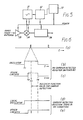
- the oscillator circuit comprises an oscillator 10, a frequency modulation circuit 11 and a temperature compensation circuit 12 as described herein by reference to Figure 2 (a).
- the oscillator circuit shown in Figure 3 (a) also includes a transient compensation circuit 13 producing a further control voltage V TC .
- the further control voltage is applied at a further control input I3 of the modulation circuit and is effective to offset the transient frequency response of oscillator 10.
- the further control voltage has a variation as a function of time which is the inverse of the transient frequency variation it is intended to offset; that is to say, the control voltage gives rise to a frequency variation which is equal to, and in the opposite sense as, the frequency variation produced by transient effects.
- a transient compensation circuit utilised in accordance with the present invention may consist solely of analogue components designed to generate a control voltage V TC when power is supplied thereto.
- the transient compensation circuit may be activated by application thereto of a suitable trigger signal, in advance of the oscillator circuit being turned off or, alternatively the oscillator circuit may be left in an uncompensated condition at switch off, especially in circumstances when the switch-on conditions are regarded as more critical.
- the transient compensation circuit could be embodied using digital circuitry used either for the purposes of triggering or in order to generate the control voltage itself.
- digital circuitry might include digital signal processing circuits or microprocessor circuits operating in association with a digital-to-analogue interface. It is envisaged that digital techniques could prove particularly useful in circumstances when the oscillator circuit is switched on shortly after it has been turned off, a situation which might give rise to modified electrical and thermal transients.
- a transient frequency-compensated oscillator circuit in accordance with the present invention finds particular, though not exclusive application, in intermittently-operated, radio frequency transmitters and receivers.
- a radio frequency transmitter or receiver is switched on for a short time and switched off for a longer time thereby enabling the average power consumption to be reduced. This is advantageous in systems that transmit status information infrequently or are not in continuous use.
- the receiver power can be reduced by intermittent or sampling operation, and the time needed to attain a stable frequency from turn-on then becomes a critical factor if a high sampling rate is required.
- the receiver has to be on for long enough to detect transmissions in the correct channel, to be switched on frequently enough to detect transmissions within a reasonable delay time (when a transmmission is detected, a continuous receiver mode can be invoked) and to have a low enough duty cycle to achieve the required power conservation. In these circumstances a transient frequency compensated oscillator circuit could prove invaluable.
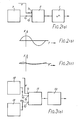
- FIG. 4 shows, in block schematic form, an example of a radio frequencer transmitter which uses a transient frequency compensation circuit to minimise the switch-on time. It includes an oscillator 21, a frequency modulator 22, and a transient compensation circuit 23.
- Figure 5 shows in block schematic form an example of part of a radio frequency receiver including an oscillator 31, a frequency modulator 32, a transient compensation circuit 33, a signal mixer 34, a radio frequency (RF) preamplifier 35, and intermediate frequency (if) circuits 36 to obtain the received signal.
- the transient compensation circuit 33 is used to operate the receiver in a sampling mode with minimum power consumption, the compensated oscillator operating as a first local oscillator.
- Figures 6a to 6e show a timing sequence illustrating how the transient compensated sampling radio frequency receiver may operate, the radio frequency receiver being switched on intermittently by a sampling gate ( Figure 6a) so that the power consumption is reduced according to the duty cycle.
- a gate signal (Figure 6b) turns on the local oscillator first, at time T1.
- the other circuits such as mixers and amplifiers, stabilise in a shorter time than the oscillator and so these circuits may be gated on ( Figure 6c) later, at time T2, thereby to minimise power consumption.
- a second local oscillator If a second local oscillator is used, it may stabilise in a sufficiently short time because of its much lower frequency, which reduces the frequency error pro rata, such that transient compensation of the kind described in accordance with this invention is unncessary; otherwise a second transient compensation circuit may be required and the second local oscillator may also have to be switched on at time T1.
- the present invention may find applications in many different fields of activity including, for example, cordless fire and security systems, paging radio receivers, personal communications systems (radios operating in a low power, stand by mode), low power radio remote control systems, radio monitoring systems and low power radio telemetry.
Landscapes
- Inductance-Capacitance Distribution Constants And Capacitance-Resistance Oscillators (AREA)
- Stabilization Of Oscillater, Synchronisation, Frequency Synthesizers (AREA)
Applications Claiming Priority (2)
| Application Number | Priority Date | Filing Date | Title |
|---|---|---|---|
| GB8824967 | 1988-10-25 | ||
| GB888824967A GB8824967D0 (en) | 1988-10-25 | 1988-10-25 | Oscillator circuit |
Publications (2)
| Publication Number | Publication Date |
|---|---|
| EP0366373A2 true EP0366373A2 (de) | 1990-05-02 |
| EP0366373A3 EP0366373A3 (de) | 1990-11-07 |
Family
ID=10645754
Family Applications (1)
| Application Number | Title | Priority Date | Filing Date |
|---|---|---|---|
| EP19890310837 Withdrawn EP0366373A3 (de) | 1988-10-25 | 1989-10-20 | Oszillator mit Kompensierung momentaner Schwankungen des Frequenzganges |
Country Status (3)
| Country | Link |
|---|---|
| EP (1) | EP0366373A3 (de) |
| CA (1) | CA2001208A1 (de) |
| GB (1) | GB8824967D0 (de) |
Family Cites Families (2)
| Publication number | Priority date | Publication date | Assignee | Title |
|---|---|---|---|---|
| JPS55118207A (en) * | 1979-03-05 | 1980-09-11 | Toshiba Corp | Non-linear type characteristic compensation system |
| JPS62202618A (ja) * | 1986-02-28 | 1987-09-07 | Nec Corp | 温度補償回路 |
-
1988
- 1988-10-25 GB GB888824967A patent/GB8824967D0/en active Pending
-
1989
- 1989-10-20 EP EP19890310837 patent/EP0366373A3/de not_active Withdrawn
- 1989-10-23 CA CA 2001208 patent/CA2001208A1/en not_active Abandoned
Also Published As
| Publication number | Publication date |
|---|---|
| GB8824967D0 (en) | 1988-11-30 |
| EP0366373A3 (de) | 1990-11-07 |
| CA2001208A1 (en) | 1990-04-25 |
Similar Documents
| Publication | Publication Date | Title |
|---|---|---|
| US5152006A (en) | Receiver controller method and apparatus | |
| EP1143606B1 (de) | Numerisch gesteuerter variabeler Oszillator | |
| EP0519145B1 (de) | Elektrischer abgestimmter RF-Empfänger, Gerät und Verfahren dafür | |
| EP0176818A2 (de) | Temperaturkompensierter Oszillator | |
| JP3186500B2 (ja) | 無線装置及び無線装置の調整方法 | |
| US9571070B2 (en) | Clock circuit for a microprocessor | |
| US20020063608A1 (en) | Dual-function connection pads for TCXO integrated circuit | |
| US7266158B2 (en) | Radio communication equipment and method for controlling same | |
| KR100290498B1 (ko) | 수정 발진기용 온도 보상 회로 및 그 제조 방법 | |
| KR960006363A (ko) | 비연속적인 수신 모드에서 동작하는 수신기에 대한 턴온 시간을 최소화하는 장치 및 방법 | |
| KR100379848B1 (ko) | 디지털온도보상발진기및그제어방법 | |
| EP1078449B1 (de) | Vorrichtung und verfahren zur reduzierung der einschaltzeit eines kristalloszillators | |
| EP1402643B1 (de) | Abstimmbare spannungsgesteuerte oszillatorschaltung mit erfassungshilfe und verfahren zum betrieb derselben | |
| EP0366373A2 (de) | Oszillator mit Kompensierung momentaner Schwankungen des Frequenzganges | |
| JP4503512B2 (ja) | 無線通信装置及び電力変換器の動作周波数制御方法 | |
| WO1992013395A1 (en) | Receiver controller method and apparatus | |
| US5418503A (en) | Compensation of transient frequency drift in oscillator circuits | |
| US7616939B2 (en) | Receiver and electronic device using the same | |
| EP3402261B1 (de) | Verfahren und vorrichtungen, die mindestens eine von einer temperatur- und frequenzabweichung angeben | |
| EP0746930B1 (de) | Frequenzstabilisierter fsk-sender | |
| EP2084811B1 (de) | Integrierte schaltung mit spannungsgeregeltem oszillator und temperatursteuerungsverfahren für einen spannungsgeregelten oszillator | |
| JP3141539B2 (ja) | 無線機とその自動周波数調整方法 | |
| KR100435557B1 (ko) | Rf-모듈의 전원 공급방법 | |
| JP2779270B2 (ja) | 無線受信装置 | |
| JP2788595B2 (ja) | レーダ・トランスポンダ |
Legal Events
| Date | Code | Title | Description |
|---|---|---|---|
| PUAI | Public reference made under article 153(3) epc to a published international application that has entered the european phase |
Free format text: ORIGINAL CODE: 0009012 |
|
| AK | Designated contracting states |
Kind code of ref document: A2 Designated state(s): AT BE CH DE ES FR GB GR IT LI LU NL SE |
|
| PUAL | Search report despatched |
Free format text: ORIGINAL CODE: 0009013 |
|
| AK | Designated contracting states |
Kind code of ref document: A3 Designated state(s): AT BE CH DE ES FR GB GR IT LI LU NL SE |
|
| STAA | Information on the status of an ep patent application or granted ep patent |
Free format text: STATUS: THE APPLICATION HAS BEEN WITHDRAWN |
|
| 18W | Application withdrawn |
Withdrawal date: 19910625 |