EP0366332A2 - Digitales Speichersystem - Google Patents
Digitales Speichersystem Download PDFInfo
- Publication number
- EP0366332A2 EP0366332A2 EP89310644A EP89310644A EP0366332A2 EP 0366332 A2 EP0366332 A2 EP 0366332A2 EP 89310644 A EP89310644 A EP 89310644A EP 89310644 A EP89310644 A EP 89310644A EP 0366332 A2 EP0366332 A2 EP 0366332A2
- Authority
- EP
- European Patent Office
- Prior art keywords
- bitline
- transistor
- pullup
- source
- terminal
- Prior art date
- Legal status (The legal status is an assumption and is not a legal conclusion. Google has not performed a legal analysis and makes no representation as to the accuracy of the status listed.)
- Granted
Links
Images


Classifications
-
- G—PHYSICS
- G11—INFORMATION STORAGE
- G11C—STATIC STORES
- G11C7/00—Arrangements for writing information into, or reading information out from, a digital store
- G11C7/06—Sense amplifiers; Associated circuits, e.g. timing or triggering circuits
- G11C7/065—Differential amplifiers of latching type
-
- G—PHYSICS
- G11—INFORMATION STORAGE
- G11C—STATIC STORES
- G11C11/00—Digital stores characterised by the use of particular electric or magnetic storage elements; Storage elements therefor
- G11C11/21—Digital stores characterised by the use of particular electric or magnetic storage elements; Storage elements therefor using electric elements
- G11C11/34—Digital stores characterised by the use of particular electric or magnetic storage elements; Storage elements therefor using electric elements using semiconductor devices
- G11C11/40—Digital stores characterised by the use of particular electric or magnetic storage elements; Storage elements therefor using electric elements using semiconductor devices using transistors
- G11C11/41—Digital stores characterised by the use of particular electric or magnetic storage elements; Storage elements therefor using electric elements using semiconductor devices using transistors forming static cells with positive feedback, i.e. cells not needing refreshing or charge regeneration, e.g. bistable multivibrator or Schmitt trigger
- G11C11/413—Auxiliary circuits, e.g. for addressing, decoding, driving, writing, sensing, timing or power reduction
- G11C11/417—Auxiliary circuits, e.g. for addressing, decoding, driving, writing, sensing, timing or power reduction for memory cells of the field-effect type
- G11C11/419—Read-write [R-W] circuits
-
- G—PHYSICS
- G11—INFORMATION STORAGE
- G11C—STATIC STORES
- G11C7/00—Arrangements for writing information into, or reading information out from, a digital store
- G11C7/12—Bit line control circuits, e.g. drivers, boosters, pull-up circuits, pull-down circuits, precharging circuits, equalising circuits, for bit lines
Definitions
- This invention relates to digital memory systems and, more specifically, to a high speed static random access memory (RAM) system.
- RAM static random access memory
- V It/C
- I the bitline charging current
- C the bitline capacitance
- a digital memory system of the type which includes an amplifier transistor connected to provide an amplified bitline signal corresponding to the state of a selected memory cell.
- the system overcomes several limitations associated with the above mentioned high speed circuits by including a bitline pullup transistor positioned to function as a current source for the bitline and as a load device for the amplifier transistor.
- the system includes a column of memory cells and a plurality of word lines connected for selecting a memory cell.
- a bitline is connected to each memory cell in the column and a bitline pullup transistor having first, second and third terminals is arranged to form a current source at the seccnd terminal.
- First and second source/drain electrodes of an amplifier transistor are connected to the second terminal of the pullup transistor and the bitline respectively.
- the gate electrode of the amplifier transistor is connected to receive a bias voltage.
- An amplified bitline signal corresponding to the state of a selected memory cell is available at an output node between the pullup and amplifier transistors.
- the preferred embodiment of the memory system includes first and second bitlines connected to each memory cell in the column.
- a bitline pullup transistor and an amplifier transistor are associated with each bit line as described above.
- An output node between the first pullup and amplifier transistors provides an amplified bitline signal corresponding to the state of a selected memory cell while a second output node between the seccnd pullup transistor and the second amplifier transistor provides an amplified bitline signal corresponding to the inverted state of a selected memory cell.
- the gate electrode of the first amplifier transistor is connected to the second source/drain electrode of the second amplifier transistor and the gate electrode of the second amplifier transistor is connected to the second source/drain electrode of the first amplifier transistor.
- These gate connections provide gate to source voltages in proportion to the difference between voltage levels of the first and second bit lines.
- the first and second pullup transistors are field effect transistors and the system further includes a diode serially connected between the bitline and a reference potential.
- high speed static random access memory operation is enhanced by isolating the capacitance of a bitline from the associated bitline pullup device.
- the pullup device functions as the sense amplifier load as well as the bitline current source to provide faster and simpler operation.
- bitline current could be used to generate a sufficiently large signal, a simpler, lower power, faster system would be available.
- speed requirements of high density memories preclude obtaining the full amplitude signal directly from the bitlines.
- a merged bitline pullup - sense amplifier circuit provides an impedance transformation, i.e., a current to voltage conversion of the bitline signal. This results in a highly amplified voltage output signal indicative of the state of a selected memory cell.
- Figure 1 is a partial schematic view of a high speed static RAM device 10 comprising a merged bitline pullup-sense amplifier circuit in conjunction with an exemplary column of 64 memory cells 12.
- the device 10 is presented in simplified form to more clearly describe the invention, it is to be understood that the device includes numerous additional components present in conventional static RAM architecture such as row and column address circuitry, decode logic and output circuitry. See U.S. Patent No. 4,665,508 which is incorporated by reference.
- the device 10 may be a 4K GaAs MESFET Static RAM containing 4,096 memory cells organized in a 64 row by 64 column array.
- Decoding may be implemented with a single level of 64 six-input NOR gates.
- the decoded 6-bit row and column addresses enable the word lines and select a particular column of memory cells. Data are sequentially written into or read out of selected memory cells in accordance with the state of the write enable, data in and chip select signals.
- the memory cells 12 illustrated in Figure 1 may each be, for example, of a conventional six transistor design including two cross-coupled switching transistors, two load transistors and a pair of pass transistors.
- a plurality of word lines WL i and bitlines BL i are connected for memory cell selection.
- bitlines BL1 and BL2 are coupled to the memory cells 12 along opposing sides of the column.
- the bitlines are coupled to a power supply line V DD by bitline pullup - sense amplifier circuitry which includes a pair of dual function pullup/load transistors 18 and 20 as well as a pair of amplifier transistors 22 and 24 each positioned between a bitline and one of the dual function transistors 18 or 20.
- An amplifier output node 28 or 30 is located between each dual function transistor 18 or 20 and an adjacent amplifier transistor 22 or 24.
- the amplifier transistors 22 and 24 are positioned to isolate the bitline capacitance from the output nodes 28 and 30. With this isolation each transistor 18 and 20 serves as the load to an adjacent amplifier transistor. The arrangement enables a very fast amplified output to be developed at the output nodes 28 and 30.
- each amplifier transistor 22 and 24 is connected to an opposing bitline and all four transistors 18, 20, 22 and 24 are depletion mode MESFETs.
- the transistors 18 and 20 are each arranged with the drain electrode coupled to V DD and the gate tied to the source electrode thereby providing a current source.
- a clamping diode 42 may be serially connected between each bitline and a reference potential 44.
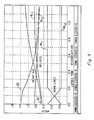
- a computer simulation has been carried out to compare the performance of the device 10 with the memory device 50 of Figure 2, which is based on a conventional sense amplifier design.
- the device 50 also includes the clamping diodes 42 of the present invention in order to obtain similar voltage swings, this permitting a more objective evaluation of the merged bitline - pullup circuitry of the present invention.
- the comparison was performed by reading data out of two adjacent memory cells 12 in a column.
- the adjacent cells were initialized to opposite states in order to require reversal of voltages in bitlines BL1 and BL2. That is, simultaneously switching WL1 and WL2 reverses the memory cell selection and causes the bitlines to charge to opposite states.
- the bitlines were assumed to each include 0.3 pF of capacitance.
- lapsed time between the word line and sense out cross points is approximately 0.1 ns shorter for the device 10.
- the rise time of the device 10 sense out signal e.g., to 90 percent of the peak to peak value, is also much shorter.
- V DD for device 50 was 2.7 volts while V DD for the device 10 was only 2.2 volts. Nevertheless, the output signal of the device 10 was much larger, i.e., approximately 0.5 volts.
- the device 10 is capable of providing output signals of acceptable magnitude faster than the device 50.
- the device 10 provides a sense out signal of 0.5 volts (as measured from the sense out cross points) in approximately 0.1 ns.
- the device 50 requires greater than a 0.5 ns rise time to develop a 0.5 volt output. ⁇ Thus higher speed memory operation is attainable with the merged bitline - pullup circuitry of the present invention.
- a corresponding method for enhancing high speed static random access memory operation comprises the step of isolating the capacitance of a bitline from the associated bitline pullup device.
- the pullup device is positioned to function as the sense amplifier load as well as the bitline current source. The result is faster and simpler memory operation.
- a feature of the preferred embodiment circuit 10 is that the gate electrode 40 of each amplifier transistor 22 and 24 is connected to an opposing bitline.
- the gate bias of each amplifier transistor could be provided with a DC voltage
- the cross coupled scheme of Figure 1 is advantageous for three reasons. First, the coupling eliminates the need for providing an external voltage bias. Second, the amplified signal response times at the output nodes 28 and 30 are nearly symmetrical in comparison to the bitline response. Third, the amplifier sensitivity is approximately doubled because the gate to source voltage of each amplifier transistor is essentially the difference between the two bitline voltages.
- the designs disclosed herein are more power efficient because the same current that charges the bitlines provides the output signal through a simple impedance transformation.
- a single bitline e.g., BL1
- one pullup/load transistor 18 and one amplifier transistor 22 provide sufficient gain for RAM operation although a longer response time may be required in order to develop a desired sense out voltage response.
- the advantages of this embodiment are lower power dissipation and fewer components.
- transistors 18, 20, 22 and 24 be of equal size, this is not necessary. Nor do the transistors have to be MESFETs. They may, for example, be replaced with MOS, bipolar or other types of devices. All of the devices 18 - 24 could be high electron mobility transistors (HEMTs). Furthermore, designs incorporating enhancement mode devices are within the scope of substitutions, although these may not provide satisfactory performance. Accordingly, the scope of the invention is only to be limited by the claims which follow.
Landscapes
- Engineering & Computer Science (AREA)
- Microelectronics & Electronic Packaging (AREA)
- Computer Hardware Design (AREA)
- Static Random-Access Memory (AREA)
Applications Claiming Priority (2)
| Application Number | Priority Date | Filing Date | Title |
|---|---|---|---|
| US262402 | 1988-10-25 | ||
| US07/262,402 US4951252A (en) | 1988-10-25 | 1988-10-25 | Digital memory system |
Publications (3)
| Publication Number | Publication Date |
|---|---|
| EP0366332A2 true EP0366332A2 (de) | 1990-05-02 |
| EP0366332A3 EP0366332A3 (de) | 1992-03-18 |
| EP0366332B1 EP0366332B1 (de) | 1995-12-20 |
Family
ID=22997345
Family Applications (1)
| Application Number | Title | Priority Date | Filing Date |
|---|---|---|---|
| EP89310644A Expired - Lifetime EP0366332B1 (de) | 1988-10-25 | 1989-10-17 | Digitales Speichersystem |
Country Status (4)
| Country | Link |
|---|---|
| US (1) | US4951252A (de) |
| EP (1) | EP0366332B1 (de) |
| JP (1) | JP2752197B2 (de) |
| DE (1) | DE68925181T2 (de) |
Families Citing this family (7)
| Publication number | Priority date | Publication date | Assignee | Title |
|---|---|---|---|---|
| JPH0793033B2 (ja) * | 1989-08-24 | 1995-10-09 | 日本電気株式会社 | センスアンプ |
| US5430677A (en) * | 1991-02-11 | 1995-07-04 | Intel Corporation | Architecture for reading information from a memory array |
| US5285408A (en) * | 1992-09-15 | 1994-02-08 | Micron Semiconductor, Inc. | Method and apparatus for providing a faster ones voltage level restore operation in a dram |
| EP0747903B1 (de) * | 1995-04-28 | 2002-04-10 | STMicroelectronics S.r.l. | Leseschaltung für Speicherzellen mit niedriger Versorgungsspannung |
| JP3967493B2 (ja) * | 1999-06-18 | 2007-08-29 | 株式会社東芝 | 半導体記憶装置 |
| US7110311B2 (en) * | 2004-06-15 | 2006-09-19 | Atmel Corporation | Sense amplifier for reduced sense delay in low power mode |
| US7161861B2 (en) * | 2004-11-15 | 2007-01-09 | Infineon Technologies Ag | Sense amplifier bitline boost circuit |
Family Cites Families (4)
| Publication number | Priority date | Publication date | Assignee | Title |
|---|---|---|---|---|
| DE2309616C2 (de) * | 1973-02-27 | 1982-11-11 | Ibm Deutschland Gmbh, 7000 Stuttgart | Halbleiterspeicherschaltung |
| US4665508A (en) * | 1985-05-23 | 1987-05-12 | Texas Instruments Incorporated | Gallium arsenide MESFET memory |
| JP2559028B2 (ja) * | 1986-03-20 | 1996-11-27 | 富士通株式会社 | 半導体記憶装置 |
| JPS62252597A (ja) * | 1986-04-24 | 1987-11-04 | Sony Corp | センスアンプ |
-
1988
- 1988-10-25 US US07/262,402 patent/US4951252A/en not_active Expired - Lifetime
-
1989
- 1989-10-17 DE DE68925181T patent/DE68925181T2/de not_active Expired - Fee Related
- 1989-10-17 EP EP89310644A patent/EP0366332B1/de not_active Expired - Lifetime
- 1989-10-24 JP JP27700289A patent/JP2752197B2/ja not_active Expired - Fee Related
Also Published As
| Publication number | Publication date |
|---|---|
| EP0366332A3 (de) | 1992-03-18 |
| EP0366332B1 (de) | 1995-12-20 |
| JPH02244493A (ja) | 1990-09-28 |
| DE68925181T2 (de) | 1996-05-02 |
| DE68925181D1 (de) | 1996-02-01 |
| US4951252A (en) | 1990-08-21 |
| JP2752197B2 (ja) | 1998-05-18 |
Similar Documents
| Publication | Publication Date | Title |
|---|---|---|
| US5371713A (en) | Semiconductor integrated circuit | |
| US4247791A (en) | CMOS Memory sense amplifier | |
| US5243573A (en) | Sense amplifier for nonvolatile semiconductor storage devices | |
| US5040146A (en) | Static memory cell | |
| US4779226A (en) | Complementary high performance cam cell | |
| EP0199501B1 (de) | CMOS-Stromdetektorverstärker | |
| US4933906A (en) | Non-volatile semiconductor memory device | |
| US4932002A (en) | Bit line latch sense amp | |
| JPH07147094A (ja) | ビット線容量分離を含む強誘電体を用いたram検出構成 | |
| US5226014A (en) | Low power pseudo-static ROM | |
| US5243569A (en) | Differential cell-type eprom incorporating stress test circuit | |
| US5453950A (en) | Five transistor memory cell with shared power line | |
| US6292418B1 (en) | Semiconductor memory device | |
| US5668485A (en) | Row decoder with level translator | |
| US4951252A (en) | Digital memory system | |
| US5898611A (en) | SRAM with high speed read/write operation | |
| JP2756797B2 (ja) | Fetセンス・アンプ | |
| US5083295A (en) | Integrated memory circuit with interconnected sense amplifiers | |
| US5022003A (en) | Semiconductor memory device | |
| US4380055A (en) | Static RAM memory cell | |
| EP0195631A2 (de) | Halbleiterspeicher | |
| US5623440A (en) | Multiple-bit random access memory cell | |
| US4899309A (en) | Current sense circuit for a ROM system | |
| US6657909B2 (en) | Memory sense amplifier | |
| JPH06333386A (ja) | 半導体記憶装置 |
Legal Events
| Date | Code | Title | Description |
|---|---|---|---|
| PUAI | Public reference made under article 153(3) epc to a published international application that has entered the european phase |
Free format text: ORIGINAL CODE: 0009012 |
|
| AK | Designated contracting states |
Kind code of ref document: A2 Designated state(s): DE FR GB IT NL |
|
| RIN1 | Information on inventor provided before grant (corrected) |
Inventor name: TADDIKEN, ALBERT HENRY Inventor name: WHITE, WILLIAM ALVIN |
|
| PUAL | Search report despatched |
Free format text: ORIGINAL CODE: 0009013 |
|
| AK | Designated contracting states |
Kind code of ref document: A3 Designated state(s): DE FR GB IT NL |
|
| 17P | Request for examination filed |
Effective date: 19920828 |
|
| 17Q | First examination report despatched |
Effective date: 19930423 |
|
| GRAA | (expected) grant |
Free format text: ORIGINAL CODE: 0009210 |
|
| AK | Designated contracting states |
Kind code of ref document: B1 Designated state(s): DE FR GB IT NL |
|
| ITF | It: translation for a ep patent filed | ||
| REF | Corresponds to: |
Ref document number: 68925181 Country of ref document: DE Date of ref document: 19960201 |
|
| ET | Fr: translation filed | ||
| PLBE | No opposition filed within time limit |
Free format text: ORIGINAL CODE: 0009261 |
|
| STAA | Information on the status of an ep patent application or granted ep patent |
Free format text: STATUS: NO OPPOSITION FILED WITHIN TIME LIMIT |
|
| 26N | No opposition filed | ||
| PGFP | Annual fee paid to national office [announced via postgrant information from national office to epo] |
Ref country code: NL Payment date: 20010921 Year of fee payment: 13 |
|
| PGFP | Annual fee paid to national office [announced via postgrant information from national office to epo] |
Ref country code: DE Payment date: 20011030 Year of fee payment: 13 |
|
| REG | Reference to a national code |
Ref country code: GB Ref legal event code: IF02 |
|
| PG25 | Lapsed in a contracting state [announced via postgrant information from national office to epo] |
Ref country code: DE Free format text: LAPSE BECAUSE OF NON-PAYMENT OF DUE FEES Effective date: 20030501 Ref country code: NL Free format text: LAPSE BECAUSE OF NON-PAYMENT OF DUE FEES Effective date: 20030501 |
|
| NLV4 | Nl: lapsed or anulled due to non-payment of the annual fee |
Effective date: 20030501 |
|
| PG25 | Lapsed in a contracting state [announced via postgrant information from national office to epo] |
Ref country code: IT Free format text: LAPSE BECAUSE OF NON-PAYMENT OF DUE FEES;WARNING: LAPSES OF ITALIAN PATENTS WITH EFFECTIVE DATE BEFORE 2007 MAY HAVE OCCURRED AT ANY TIME BEFORE 2007. THE CORRECT EFFECTIVE DATE MAY BE DIFFERENT FROM THE ONE RECORDED. Effective date: 20051017 |
|
| PGFP | Annual fee paid to national office [announced via postgrant information from national office to epo] |
Ref country code: GB Payment date: 20070918 Year of fee payment: 19 |
|
| REG | Reference to a national code |
Ref country code: FR Ref legal event code: ST Effective date: 20080630 |
|
| PGFP | Annual fee paid to national office [announced via postgrant information from national office to epo] |
Ref country code: FR Payment date: 20061003 Year of fee payment: 18 |
|
| PG25 | Lapsed in a contracting state [announced via postgrant information from national office to epo] |
Ref country code: FR Free format text: LAPSE BECAUSE OF NON-PAYMENT OF DUE FEES Effective date: 20071031 |
|
| GBPC | Gb: european patent ceased through non-payment of renewal fee |
Effective date: 20081017 |
|
| PG25 | Lapsed in a contracting state [announced via postgrant information from national office to epo] |
Ref country code: GB Free format text: LAPSE BECAUSE OF NON-PAYMENT OF DUE FEES Effective date: 20081017 |