EP0365721B1 - Mémoire à semi-conducteur programmable - Google Patents
Mémoire à semi-conducteur programmable Download PDFInfo
- Publication number
- EP0365721B1 EP0365721B1 EP88309995A EP88309995A EP0365721B1 EP 0365721 B1 EP0365721 B1 EP 0365721B1 EP 88309995 A EP88309995 A EP 88309995A EP 88309995 A EP88309995 A EP 88309995A EP 0365721 B1 EP0365721 B1 EP 0365721B1
- Authority
- EP
- European Patent Office
- Prior art keywords
- column
- semiconductor memory
- voltage
- coupled
- programmable semiconductor
- Prior art date
- Legal status (The legal status is an assumption and is not a legal conclusion. Google has not performed a legal analysis and makes no representation as to the accuracy of the status listed.)
- Expired - Lifetime
Links
Images


Classifications
-
- G—PHYSICS
- G11—INFORMATION STORAGE
- G11C—STATIC STORES
- G11C16/00—Erasable programmable read-only memories
- G11C16/02—Erasable programmable read-only memories electrically programmable
- G11C16/06—Auxiliary circuits, e.g. for writing into memory
- G11C16/10—Programming or data input circuits
- G11C16/14—Circuits for erasing electrically, e.g. erase voltage switching circuits
-
- G—PHYSICS
- G11—INFORMATION STORAGE
- G11C—STATIC STORES
- G11C16/00—Erasable programmable read-only memories
- G11C16/02—Erasable programmable read-only memories electrically programmable
- G11C16/06—Auxiliary circuits, e.g. for writing into memory
- G11C16/08—Address circuits; Decoders; Word-line control circuits
-
- G—PHYSICS
- G11—INFORMATION STORAGE
- G11C—STATIC STORES
- G11C16/00—Erasable programmable read-only memories
- G11C16/02—Erasable programmable read-only memories electrically programmable
- G11C16/06—Auxiliary circuits, e.g. for writing into memory
- G11C16/10—Programming or data input circuits
- G11C16/12—Programming voltage switching circuits
-
- G—PHYSICS
- G11—INFORMATION STORAGE
- G11C—STATIC STORES
- G11C16/00—Erasable programmable read-only memories
- G11C16/02—Erasable programmable read-only memories electrically programmable
- G11C16/06—Auxiliary circuits, e.g. for writing into memory
- G11C16/30—Power supply circuits
Definitions
- This invention generally relates to a programmable semiconductor memory using non-volatile transistors as memory cells from which data can be electrically erased. It particularly but not exclusively relates to a non-volatile semiconductor memory in which data stored in a plurality of memory cells may be erased simultaneously or in units of a row. Data may be written to the memory a cell (or bit) at a time.
- EPROMs Erasable and Programmable Read Only Memories
- E 2 PROMs Electrically erasable PROMS
- E 2 PROMs have been developed which permit the simultaneous erasure of data stored in a plurality of memory cells. Such an E 2 PROM is disclosed in "A 128K Flash EEPROM Using Double Polysilicon Technology", pp. 76-77 of "1987 IEEE International Solid State Circuits Conference, Digest of Technical Papers.”
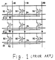
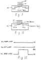
- FIG. 1 Is a circuit diagram depicting a memory cell array of a prior art E 2 PROM in which the data stored in the memory cells may be erased simultaneously.
- memory cells 50 consist of non-volatile transistors having a floating gate electrode, a control gate electrode and an erase gate electrode. Data erasure may be effected electrically.
- Memory cells 50 are arranged in rows (disposed vertically) and columns (disposed horizontally). The drains of the memory cells 50 in a given column are commonly connected to one of bit lines 51. The sources of the memory cells 50 in a given column are commonly connected to one of ground lines 52.
- the control gate electrodes of the memory cells 50 in a given row are commonly connected to one row lines 53.
- the erase gate electrodes of the memory cells 50 in a given column are commonly connected to one of erase lines 54.
- Such a memory cell array is disclosed in US Patent No 4,437,174.
- each memory cell consists of a single non-volatile transistor which may contain a single bit of data.
- Each memory cell is connected to a corresponding bit line, ground line, row line and erase line.
- four wires namely, the bit line, ground line, row line and erase line, are required for each bit.
- the drain of each cell consists of a diffusion region and the bit line consists of a metal wire of, for example, aluminium.
- JP-A-62 219 296 Another memory wherein non volatile memory cells are arranged in a row and column matrix and wherein the cells in a given column are series connected is disclosed in JP-A-62 219 296.
- US-A-4 648 074 discloses a memory device according to the preamble of claim 1.
- US-A-4 485 349 discloses use of ground potential to control gates of non-selected floating gate memory cells in a given row line.
- the present invention overcomes the above-noted problems of the prior art by reducing the number of wires required for each bit or cell and reducing the number of contacts coupling the cells to the bit lines.
- the programmable semiconductor memory of this invention comprises a plurality of series circuit units arranged in a row and column matrix with each series circuit unit having at least two memory cells connected in series.
- Each memory cell consists of a non-volatile transistor having a control gate electrode, a floating gate electrode, and an erase gate electrode. Data stored in the memory cells may be erased electrically.
- One end of each series circuit unit is coupled to a bit line, the circuit units in a given row of circuit units being coupled to the same bit line.
- the control gate electrodes of the memory cells in a given column of memory cells are coupled to the same column line and the erase gate electrodes of the memory cells in a given series circuit unit are commonly coupled to an erase line, the circuit units in a given row of circuit units being coupled to the same erase line.
- An advantage of the described embodiment of this invention is that a non-volatile semiconductor memory is provided wherein a high integration density can be achieved by reducing the number of wires and the number of contacts.
- Another advantage is that a non-volatile semiconductor memory with a low manufacturing cost.
- Yet another advantage is that a non-volatile semiconductor memory is provided which permits an increased production yield.
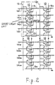
- FIG. 2 is a circuit diagram of a memory cell array in which the present invention is applied to an E 2 PROM (hereafter referred to simply as "memory").
- series circuit unit 10 includes four memory cells 11 connected in series.
- Each memory cell 11 of series circuit unit 10 consists of a non-volatile transistor having: a source region; a drain region; a floating gate electrode arranged above the channel region between the source and drain regions; a control gate electrode; and an erase gate electrode arranged so as to overlap the floating gate electrode. Data stored in a memory cell 11 may be erased electrically.
- Programmable memory refers to any kind of semiconductor memory which can be programmed after fabrication or manufacture. It may include, but should not be limited to, non-volatile memories, SRAMs, and DRAMs.
- each column of series circuit units in Figure 2 includes four columns of memory cells, the control gates of the memory cells disposed in a given column of memory cells being coupled to the same one of column lines 14.
- each series circuit unit 10 is coupled to one of bit lines 12 1 , ... 12 N , with the series circuit units in a given row of series circuit units being coupled to the same bit line.
- the other end of each series circuit unit 10 is coupled to one of ground lines 13 1 ,... 13 M , with the series circuit units in a given column of series circuit units being coupled to the same ground line.
- a voltage of OV is maintained across ground lines 13.
- the erase gate electrodes of each memory cell in a series circuit unit are coupled to a common erase line 15, with the series circuit units in a given row being coupled to the same erase line.
- the control gate electrode of each memory cell in a series circuit unit is coupled to a column line 14, with each memory cell in a given column of memory cells being coupled to the same column line.
- column lines 14 1 , 14 2 , 14 3 , 14 4 are coupled respectively to each of the four memory cells comprising a series circuit unit.
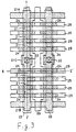
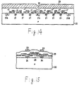
- Figure 3 is a plan view corresponding to the structure of the memory cell array circuit shown in Figure 2 when such a memory is actually provided on a semiconductor chip.
- Figure 4 is a cross-sectional view along the line I - I' in Figure 3.
- Figure 5 is a cross-sectional view along the line II- II' in Figure 3.
- a P-type silicon semiconductor substrate is used as the substrate 20 of the memory.
- N + regions 21A and 21B are used as ground lines 13.
- Metal wires 23 of aluminum, for example, are coupled through contact holes 22 to each of the N + type regions 21C located between N + regions 21A and 21B. Metal wires 23 are used as bit lines 12.
- each series circuit unit 10 consists of four memory cells 11 connected in series. In practice various numbers of memory cells may be used e.g. 8, 16 or 32, and the invention should not be understood as limited in this respect.
- One end of each series circuit 10 is coupled to a bit line 12 which is embodied in metal wire 23 while the other end is coupled to a ground line 13 which is embodied in N + region 21A or 21B.
- the control gate electrode of each memory cell 11 is coupled to a column line 14 embodied in electrode 25 and the erase gate electrode of each memory cell 11 is coupled to an erase line 15.
- Figure 6 is a circuit diagram showing the overall construction of this embodiment together with its peripheral circuitry.
- the series circuit units are disposed in a matrix of M columns and N rows, with each of the M columns of circuit units having four column lines designated 14 1n , 14 2n , 14 3n , 14 4n where n is the column number.
- Bit lines 12 are connected to row decoder 16 while the four column lines 14 associated with a given column of series circuit units are connected to the corresponding column decoder 17.
- Pulled up voltages, produced by pull-up circuit 18 by pulling-up the power source voltage Vcc and the high voltage Vpp supplied from external sources, are supplied to each column decoder 17 1 to 17 M .
- Erase lines 15 are connected to erase voltage generating circuit 19.
- a typical power source voltage Vcc is 5V and a typical high voltage Vpp is 12.5V.
- the pulled-up voltages provided by pull-up circuit 18 are 5-10V and 20V respectively.
- Erase voltage generating circuit 19 generates an erase voltage of about 20V from the high voltage Vpp and selectively outputs this to erase lines 15.
- the series circuit unit 10 containing the selected cell is coupled to bit line 12 1 and the four column lines 14 11 to 14 41 .
- the selected cell itself is coupled to column line 14 21 .
- a voltage in the range 2V to 5V would be applied to column line 14 21 .
- the voltage applied to the remaining three column lines would be in the range 5 to 10V.
- each memory cell 11 has had its threshold voltage set in accordance with what was written to it previously in a data write mode.
- a voltage in the range 2V to 5V is higher than the low threshold voltage of the cell just after erasure but lower than the high threshold voltage of the cell after a level "1" has been written to it.
- a voltage in the range 5V to 10V is sufficiently higher than the high threshold voltage of the cell after a level "1" has been written to it. Consequently, applying the voltages described to the four column lines 14 11 to 14 41 has the effect of turning ON the three memory cells whose control gate electrodes are connected to voltage in the range of 5-10V, namely those cells on column lines 14 11 , 14 31 , and 14 41 .
- the ON or OFF state of the selected cell, whose control gate electrode is connected to column line 14 21 is determined by its threshold voltage which, as noted above, is set during the data write mode.
- a 2V read voltage is applied to bit line 12 1 in response to the output of row decoder 16. If the threshold voltage of the selected transistor is low, corresponding to a level "0" state, the selected transistor is turned on by the voltage of column line 14 21 . Thus, the read voltage of 2V applied to bit line 12 1 is discharged to ground line 13 1 through series circuit unit 10. The ground lines 13, as previously noted, are maintained at OV. However, if the threshold voltage of the selected transistor is high, corresponding to a level "1" state, the transistor remains off when the voltage of column line 14 21 is applied. Thus, the read voltage of 2V applied to bit line 12 1 is not discharged to ground line 13.
- the voltage of a bit line 12 depends on whether the threshold voltage of the selected cell is high or low.
- the discrimination of logic levels "1" and “0” can thus be performed by amplifying the potential difference with a sense amplifier 30 connected to bit line 12.
- the voltage applied during data reading to the column lines 14 of the non-selected cells should normally be set at about 8V.
- a pulled-up voltage of 10V is applied from pull up circuit 18 to the column line coupled to the control gate electrode of the selected cell while a pulled-up voltage of 20V is applied to the remaining three column lines.
- the outputs of all other column decoders 17 are 0V.
- the series circuit unit 10 containing the selected cell is coupled to bit line 12 1 and the selected cell is coupled to column line 14 21 .
- a voltage of 10V is applied to column line 14 21 .
- a voltage of 20V is applied to the three remaining column lines.
- two different voltage levels are applied to bit line 12 1 depending on the write data that is being output from row decoder 16. When writing a level "1", a voltage of 10V is applied to bit line 12 1 , while a voltage of 0V is applied when writing a level "0".
- the three memory transistors 11 whose control gate electrodes are coupled to the 20V by the three column lines 14 11 , 14 31 , 14 41 operate as triodes i.e., in their non-saturation state. In this operation, a channel region is formed between the source and drain regions, as shown in Figure 9.
- the selected memory transistor whose control gate electrode is supplied with a voltage of 10V by the column line 14 21 , is driven to its saturated state, as shown in Figure 10. If 10V is applied between the bit line 12 1 and the ground line 13 1 , electrons flow from the source region of the four cells 11 in the series circuit unit 10 towards the drain region. The electric field is concentrated in the depletion layer 31 generated, particularly in the vicinity of the drain region of the selected memory transistor 11. As a result, electrons are accelerated and given sufficient energy to cross the energy barrier of the insulating film from the surface of substrate 20 in Figure 10. These electrons are called "hot electrons". They are drawn toward the control gate electrode 25 of the selected cell which is set to the voltage of 10V and fly into the floating gate electrode where they are captured. As a result, the floating gate electrode 24 of the selected cell becomes negatively charged, causing the threshold voltage to rise to a high level.
- bit line 12 1 If a voltage of 0V is applied to bit line 12 1 , the hot electrons are not generated and the threshold voltage stays in its original low state. Thus, data may be written to each individual cell.
- erasure of cell data in series circuits 10 can be effected in units of rows by selectively applying the high voltage of 25V from erase voltage generating circuit 19 only to particular erase lines 15.
- data may be read and written in bit units and may be erased either simultaneously from all the cells or in units of rows. More importantly, these processes can be carried out in an array requiring one bit line and one erase line per series circuit unit, which in the above embodiment, comprises four cells. This is in marked contrast to prior art arrays where a bit line and an erase line were required for each bit or cell.
- utilizing the present invention it is possible to produce memory cell arrays with a high integration density.
- fewer contacts are required to connect the cells with the bit line.
- the present invention requires one contact with the bit line for every four cells. This can lead to an increase in production yield.
- Figures 12 to 15 show another embodiment of this invention.
- Figure 12 is a circuit diagram showing the overall construction of this embodiment together with its peripheral circuitry.
- series circuit unit 10 consists of four cells 11 connected in series. Again, in practice various numbers of cells may be used and this embodiment should not be understood as limited in this respect.
- the cells 11 comprise the series connection of a floating gate electrode transistor having an erase gate electrode with an enhancement type MOS transistor.
- Figure 13 is a plan view of the pattern of the structure of the memory cell array in Figure 12.
- Figure 14 is a cross-sectional view along the line I - I′ in Figure 13.
- Figure 15 is a cross-sectional view along the line II - II′ in Figure 13.
- Each of the memory cells 11 comprising series circuit unit 10 includes a non-volatile transistor having: a source region; a drain region; a floating gate electrode arranged above the channel region along part of the channel length between the source and drain region; a control gate electrode provided over the floating gate electrode and across the channel region where the floating gate electrode is not provided; and an erase gate electrode arranged so as to overlap the floating gate electrode.
- the control gate of the non-volatile transistor also functions as the gate electrode of the enhancement type MOS transistor connected in series.
- electrodes 24, made of a first polycrystalline silicon layer and put in a floating electrical state are formed over the channel region between adjacent N + type regions 21 along part of the channel length and are insulated therefrom by an insulating film. Electrodes 24 are the floating gate electrodes of each memory cell 11. Electrodes 25, made of a third polycrystalline silicon layer, are formed over the plurality of electrodes 24, insulated therefrom by an insulating film, and over the channel regions where the electrodes 24 are not provided. Electrodes 25 are the control gate electrodes and the gate electrodes of the enhancement MOS transistor and serve as the column line 14 of each memory cell 11. Electrodes 26, made of a second polycrystalline silicon layer, are formed between adjacent rows of series circuit units 10, insulated therefrom by an insulating film.
- Electrodes 26 overlap part of electrodes 24 which, as noted, are the floating gate electrodes of each cell. Electrodes 26 are the erase gate electrodes and serve as the erase line 15 of each memory cell 11. In this embodiment, the enhancement MOS transistor is switched by the signal of control gate electrode 25 of the floating gate transistor during the reading and writing modes.
- This invention is not restricted to the above embodiments and may be modified in various ways.
- a voltage in the range of 2V to 5V was applied to the column line 14 that was coupled to the selected cell, while a voltage in the range 5V to 10V was applied to the remaining three column lines.
- These voltages should be set in accordance with the threshold voltage corresponding to the level "1" and level "0" of memory cell 11.
- the 2V read voltage applied to bit line 12 may also be altered as required. It is desirable to set this read voltage as low as possible to suppress what is known as the "soft write” phenomenon during the read mode.
- series circuit unit 10 comprises four memory cells in series
- the series connection of 8, 16 or 32 memory cells may be employed. If, for example, series circuit 10 comprises 8 memory cells in series, the degree of integration may be increased 2 or more times over that of the prior art memory. This combined with the increase in the density of circuit integration can result in a considerable reduction in costs.
- the electrodes 25 in Figure 3 serving as the control gate electrodes and column lines 14 of each cell, were made of a polycrystalline silicon.
- other high melting-point metallic silicides such as titanium silicide, molybdenum silicide, or other melting-point metals, may be used.
- Figures 16-23 illustrate the details of the peripheral circuitry associated with the embodiments of Figures 6 and 12 and will now be discussed.
- Figure 16 is a circuit diagram of the entire circuit, showing in detail that portion of a column decoder 17 which applies a high voltage of 10V or 20V to the column lines 14 in order to write data into the memory shown in Figures 6 and 12.
- One of column decoders 17 1 to 17 M is activated by a 4-bit address consisiting of bits A3, A4, A5, and A6.
- the decoded output of the activated column decoder 17 selects a plurality of series circuits 10 coupled together in the corresponding column of series circuit units.
- one of the four column lines coupled to this plurality of series circuits 10 is selected by a 2-bit address consisting of bits A1 and A2.
- Each column decoder 17 is provided with a column group decoder (CGD) 33 coupled to receive the 4-bit address, i.e., a combination of address bits A3, A4, A5, and A6, each bit having either a positive or negative phase.
- the decoded output of CGD 33, CG is supplied to column-group decoder buffer (CGDB) 34. It is simultaneously supplied to the four decoder-output buffers (DOPBs) 32 1 to 32 4 , which are provided for each of the four column lines 14 and which output the high voltage of 10V or 20V.
- DOPBs decoder-output buffers
- the output CGS of CGDB 34 is also supplied to DOPBs 32 1 to 32 4 .
- Each column decoder 17 is also provided with four column part decoders (CPDs) 35 1 to 35 4 , each coupled to receive the 2-bit address, i.e., a combination of address bits A1 and A2, each bit having either a positive or negative phase.
- the decoded outputs CD1 to CD4 of CPDs 35 1 to 35 4 are supplied to the corresponding one of DOPBs 32 1 to 32 4 .
- DOPBs 32 1 to 32 4 output the high voltage of 10V or 20V or a ground voltage of 0V to the corresponding column line 14 in response to the output CG of CGD 33, the output CGS of CGDB 34, and the outputs of CPDs 35.
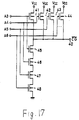
- FIG. 17 is a circuit diagram showing, in detail, the CGD 33 provided for each column decoder 17.
- CGD 33 comprises four P-type MOS transistors 41 to 44 and four N-type MOS transistors 45 to 48.
- Transistors 41 to 44 are connected in parallel, each coupled between power-source voltage terminal Vcc and node 40 for the output signal CG.
- Address bits A3, A4, A5, and A6 are supplied to the gates of MOS transistors 41 to 44, respectively.
- Transistors 45 to 48 are connected in series, coupled between output node 40 and the ground.
- Address bits A3, A4, A5, and A6 are supplied to the gates of these transistors 45 to 48, respectively.
- the CGDs 33 provided in other column decoders 17 have the same structure, but the phase of address bits A3, A4, A5, and A6 differ.
- Figure 18 is a circuit diagram showing, in detail, CGDB 34 provided for each column decoder 17.
- N-type MOS transistor 52 is coupled between nodes 50 and 51. High voltage Vpp2 is applied to node 50.
- An N-type MOS transistor 54 is connected between node 51 and node 53 for output signal CGS. The gate of transistor 52 is also coupled to node 53. The gate of transistor 54 is coupled to node 51.
- Capacitor 55 comprising an N-type MOS transistor is connected, at one end, to node 51. The other end of capacitor 55 is coupled to node 56 for receiving clock signal 1C.
- Depletion-type N-type MOS transistor 57 is connected, at one end, to node 53.
- CMOS inverter 60 is comprised of P-type MOS transistor 58 and N-type MOS transistor 59 and is coupled to receive the decoded output CG of CGD 33. Voltage Vcc is supplied to the gate of depletion-type transistor 57 at all times. All transistors used in this circuit, except for transistor 57, are enhancement-type.
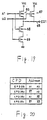
- Figure 19 is a circuit diagram showing, in detail, one of the CPDs 35 provided in each column decoder 17. More precisely, it depicts CPD 35 1 to which address bits A1 and A2 are input.
- Two P-type MOS transistors 66 and 67 are connected in parallel, each coupled between power-source voltage terminal Vcc and node 65 for output signal CD1.
- Address bits A1 and A2 are supplied to the gates of transistors 66 and 67 respectively.
- N-type MOS transistors 68 and 69 are connected in series, coupled between node 65 and the ground.
- Address bits A1 and A2 are supplied to the gates of transistors 68 and 69 respectively.
- the other CPDs 35 have the same structure as the CPD shown in Figure 19, but the phases of the input address bits differ. As shown in Figure 20, bits A1 and A2 are input to CPD 35 2 ; bits A1 and A2 are input to CPD 35 3 ; and bits A1 and A2 are input to CPD 35 4 .
- Figure 21 is a circuit diagram showing, in detail, one of DOPBs 32 provided in each column decoder 17.
- N-type MOS transistor 72 is coupled between nodes 70 and 71. High voltage Vpp2 is supplied to node 70.
- N-type MOS transistor 74 is coupled between node 71 and node 73. The gate of transistor 72 is coupled to node 73 and the gate of transistor 74 is coupled to node 71.
- Capacitor 75 comprising an N-type MOS transistor is coupled, at one end, to node 71. The other end of capacitor 75 is connected to node 76 to which clock signal o1C is supplied.
- Deletion-type, N-type MOS transistor 77 is connected, at one end, to node 73.
- Voltage Vcc is always supplied to the gate of transistor 77.
- the other end of transistor 77 is connected to the output node of CMOS inverter 80 comprising P-type MOS transistor 78 and N-type MOS transistor 79 and which is coupled to receive the decoded output CDi of CPD 35i.
- two P-type MOS transistors 82 and 83 are connected in series between nodes 70 and 81.
- Node 81 is coupled to column line 14.
- Two N-type MOS transistors 85 and 86 are connected in series between nodes 81 and 84.
- High voltage Vpp1 is supplied to node 84.
- the gate of MOS transistor 82 is coupled through inverter 88 to node 87, to which signal CGS output from CGDB 34 is supplied.
- the gate of transistor 86 is directly connected to node 87.
- the gates of transistors 83 and 85 are coupled to node 73.
- N-channel MOS transistor 89 is coupled between node 81 and the ground. The gate of transistor 89 is coupled to receive signal CG from CGD 33. All transistors used in this circuit, except for transistor 77, are enhancement-type.
- CPD 35 1 shown in Figure 19 two address bits A1 and A2 are set to level “1", turning N-type MOS transistors 68 and 69 on. Therefore, node 64 is discharged via transistors 68 and 69, and signal CD1 is also set to level "0", i.e., 0V.
- one of address bits A1 or A2 is set to level "0".
- signals CD2 to CD4 are set to level "1", i.e., Vcc.
- the output signal CGS of CGDB 34 is set to a voltage equal to or higher than Vpp2. More specifically, in CGDB 34 shown in Figure 18, the output node 61 of CMOS inverter 60 is set to "1" (Vcc) when signal CG is set to "0". Since voltage Vcc is applied to the gate of depletion-type transistor 57, node 53 is also set to “1” (Vcc). Transistor 52 is thereby turned on, and node 51 is quickly charged with the high voltage Vpp2 applied to node 50. Thus, transistor 54 is also turned on and node 53 is charged with high voltage Vpp2.
- the signal CGS obtained at node 53 is set to a level equal to or higher than Vpp2.
- DOPB 32 1 which receives the output CG of CGD 33, the output CGS of CGDB 34, and the output CD1 of CDP 35 1 , outputs a high voltage Vpp1 of 10V to the selected row line 14 11 . More specifically, in DOPB 32 shown in Figure 21, transistor 86 is turned on since signal CGS is set to a high voltage of 20V or more. The output of inverter 88, to which signal CGS is input, is set to "0". Hence, transistor 82 is also turned on. Since the decoded output CD1 of CPD 35 1 is "0" at this time, a high voltage of 20V or more is output to node 73, as in the circuit of Figure 18. As a result, transistor 85 is turned on.
- node 81 is charged with voltage Vpp1 through transistors 86 and 85. Since a high voltage of 20V or more is applied to the gates of both transistors 86 and 85 at this time, Vpp1 of 10V is applied directly to node 81.
- DOPBs 32 1 to 32 4 In each of other DOPBs 32 1 to 32 4 provided in column decoder 17 1 , which are coupled to the column lines other than selected row line 14 11 , the decoded outputs CD2 to CD4 of CPD 35 2 to 35 4 are set to "1", and node 73 is set to the ground voltage. Therefore, in the circuit of Figure 21, transistor 83 is turned on, transistor 85 is turned off, and node 81 is charged with voltage Vpp2 through transistors 82 and 83. Hence, DOPBs 32 2 to 32 4 of column decoder 17 1 output a high voltage 20V to column lines 14 21 , 14 31 , and 14 41 , respectively.
- the decoded output CG of CGD 33 is set to "1", turning the transistor 89 provided in each DOPB 32 ( Figure 21) on.
- the output voltage of DOPB 32 is 0V, i.e., the ground voltage.
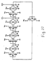
- FIG 22 is a circuit diagram showing an oscillation circuit for generating clock signal 1C and clock signal 2C (described later), for use in the circuits of Figures 18 and 21.
- This oscillation circuit is known in the prior art as a ring oscillator. It comprises an odd number of CMOS inverters 90, for example five, connected in cascade and each made of a P-type and N-type MOS transistor. Transfer gates 91 are connected between these inverters and function as resistive elements, each comprising a P-type and an N-type MOS transistor. Capacitors 92 are coupled to the connection point of the adjacent CMOS inverter and transfer gate.
- FIG 23 is a circuit diagram illustrating a PULL UP circuit for generating high voltages Vpp1 and Vpp2 used in column decoder 17.
- This circuit is of the well-known charge-pump type. It comprises a plurality of PULL UP units connected in cascade. Each unit comprises an N-type MOS transistor 95 functioning as a load transistor, N-type MOS transistor 96 functioning as a rectifying transistor, and a capacitor 97. Clock signals 1C and 2C, which have been obtained by the oscillation circuit shown in Figure 22, are alternately input to one end of capacitor 97.
Landscapes
- Read Only Memory (AREA)
Claims (19)
- Mémoire à semiconducteurs programmable comprenant:un ensemble de cellules de mémoire (11), dans lequel chaque cellule de mémoire (11) consiste en un transistor non volatil ayant une électrode de grille de commande (25);un ensemble de lignes de bit (12); etun ensemble de lignes de colonne (14);l'ensemble de cellules de mémoire (11) ayant la configuration d'un ensemble d'unités de circuit (10) disposées en une matrice de lignes et de colonnes, chaque unité de circuit (10) comprenant au moins deux cellules de mémoire (11) respectives connectées en série, une extrémité de chaque unité de circuit (10) étant couplée à l'une respective des lignes de bit (12), de façon que les cellules de mémoire (11) dans une colonne donnée aient leurs électrodes de grille de commande (25) couplées à la mêne ligne de colonne (14), mais que les cellules de mémoire (11) dans une unité de circuit (10) donnée puissent être commandées indépendamment par le fait qu'elles sont couplées à une ligne de colonne (14) différente respective; etdes moyens de décodage (16, 17) réagissant à des données d'adresse de façon à sélectionner une cellule de mémoire (11) dans l'une des unités de circuit (10) par l'application de tensions aux lignes de colonne (14) et aux lignes de bit (12), ces moyens de décodage comprenant des moyens de décodage de colonne (17) qui réagissent aux données d'adresse en appliquant une première tension à la ligne de colonne (14) couplée a la cellule sélectionnéee (11) de l'une des unités de circuit (10), et une seconde tension, différente de la premiére tension, aux lignes de colonne couplées aux cellules de mémoire (11) non sélectionnées de l'unité de circuit (10) précitée, caractérisée en ce que les transistors non volatils ont des électrodes de grille flottante (24) et en ce que les moyens de décodage de colonne (17) appliquent une tension de masse, différente des première et seconde tensions, à toutes les autres lignes de colonne (14).
- Mémoire à semiconducteurs programmable selon la revendication 1, caractérisée en outre en ce que les moyens de décodage de colonne (17) comprennent un ensemble de décodeurs de colonne (17n), chacun d'eux étant muni d'un décodeur de groupes de colonnes (33) couplé de façon à recevoir des données d'adresse et adapté pour appliquer un signal de sortie décodé à un amplificateur-séparateur de décodeur de groupe de colonnes (34) et a des amplificateurs-séparateurs de sortie de décodeur (32), chaque décodeur de colonne (17n) comportant également des décodeurs de partie de colonne (35), chacun d'eux étant couplé de façon à recevoir des données d'adresse, et à fournir des signaux de sortie décodés à l'un correspondant des amplificateurs-séparateurs de sortie de décodeur (32) (figure 16).
- Mémoire à semiconducteurs programmable selon l'une quelconque des revendications précédentes, caractérisée en outre en ce que chaque cellule de mémoire comprend une électrode de grille d'effacement (26) pour effacer électriquement des données enregistrées dans la cellule (11).
- Mémoire à semiconducteurs programmable selon l'une quelconque des revendications précédentes, caractérisée en outre en ce qu'une seconde extrémité de chaque unité de circuit (10) est couplée à une ligne de source d'alimentation (13) fournissant un potentiel prédéterminé.
- Mémoire à semiconducteurs programmable selon la revendication 4, caractérisée en outre en ce que la ligne de source d'alimentation est une ligne de masse.
- Mémoire à semiconducteurs programmable selon l'une quelconque des revendications précédentes, caractérisée en outre en ce que chaque unité de circuit comprend quatre transistors non volatils (11).
- Mémoire à semiconducteurs programmable selon l'une quelconque des revendications 1-5, caractérisée en outre en ce que chaque unité de circuit (10) comprend huit transistors non volatils (11).
- Mémoire à semiconducteurs programmable selon l'une quelconque des revendications 1-5, caractérisée en outre en ce que chaque unité de circuit (10) comprend seize transistors non volatile (11).
- Mémoire à semiconducteurs programmable selon l'une quelconque des reventications 1-5, caractérisée en outre en ce que chaque unité de circuit (10) comprend trente-deux transistors non volatils (11).
- Mémoire à semiconducteurs programmable selon l'une quelconque des revendications précédentes, caractérisée en outre en ce que les transistors non volatils sont des transistors à canal n (11).
- Mémoire à semiconducteurs programmable selon l'une quelconque des revendications précédentes, caractérisée en outre en ce que les lignes de colonne (14) consistent en silicium polycristallin.
- Mémoire à semiconducteurs programmable selon l'une quelconque des revendications 1-10, caractérisée en outre en ce que les lignes de colonne (14) consistent en un siliciure à point de fusion élevé.
- Mémoire à semiconducteurs programmable selon l'une quelconque des revendications précédentes, caractérisée en outre en ce que le siliciure a point de fusion élevé consiste en siliciure de titane.
- Mémoire à semiconducteurs programmable selon la revendication 12, caractérisée en outre en ce que le siliciure à point de fusion élevé consiste en siliciure de molybdène.
- Mémoire à semiconducteurs programmable selon la revendication 1, caractérisée en outre en ce que la première tension fait passer la cellule de mémoire sélectionnée (11) dans une unité de circuit (10) dans son état de saturation, et la seconde tension fait passer les cellules de mémoire (11) restantes dans l'unité de circuit (10) dans leur état de non saturation.
- Mémoire à semiconducteurs programmable selon la revendication 1 ou la revendication 15, caractérisée en outre en ce que pendant la lecture de données dans la cellule de mémoire (11) sélectionnée, la première tension est supérieure a une tension de seuil d'un transistor non volatil (11) correspondant à un niveau «0», et inférieure à une tension de seuil du transistor non volatil (11) correspondant à un niveau «1», et la seconde tension est supérieure à la tension de seuil correspondant à un niveau «1».
- Mémoire à semiconducteurs programmable selon l'une quelconque des revendications 1, 15 ou 16, caractérisée en outre en ce que la seconde tension qui est appliquée aux lignes de colonne (14) restantes est générée par un circuit d'élévation de tension (18) qui élève une tension de source d'alimentation externe.
- Circuit de mémoire à semiconducteurs programmable selon l'une quelconque des revendications précédentes, caractérisé en outre en ce que chaque unité de circuit (10) comprend L cellules de mémoire connectées en série, l'ensemble d'unités de circuit (10) étant organisé en une matrice de colonnes et de rangées de dimensions M x N, chaque rangé d'unités de circuit (10) étant associée à l'une respective des N lignes de bit (12), et en ce que les unités de circuit (10) dans une rangée donnée d'unités de circuit (10) sont couplées à la ligne de bit (12) associée, et les cellules de mémoire (11) dans des unités de circuit (10) qui sont couplées à la même ligne ce bit (12), sont couplées à l'une différente de M x L lignes de colonne (14).
- Dispositif de mémoire à semiconducteurs programmable selon la revendication 1, caractérisé en outre en ce que les moyens décodeurs (16, 17) comprennent des moyens décodeurs de rangée (16) associés à chaque rangée d'unités de circuit (10).
Priority Applications (2)
| Application Number | Priority Date | Filing Date | Title |
|---|---|---|---|
| EP88309995A EP0365721B1 (fr) | 1988-10-24 | 1988-10-24 | Mémoire à semi-conducteur programmable |
| DE19883855444 DE3855444T2 (de) | 1988-10-24 | 1988-10-24 | Programmierbarer Halbleiterspeicher |
Applications Claiming Priority (1)
| Application Number | Priority Date | Filing Date | Title |
|---|---|---|---|
| EP88309995A EP0365721B1 (fr) | 1988-10-24 | 1988-10-24 | Mémoire à semi-conducteur programmable |
Publications (2)
| Publication Number | Publication Date |
|---|---|
| EP0365721A1 EP0365721A1 (fr) | 1990-05-02 |
| EP0365721B1 true EP0365721B1 (fr) | 1996-07-24 |
Family
ID=8200259
Family Applications (1)
| Application Number | Title | Priority Date | Filing Date |
|---|---|---|---|
| EP88309995A Expired - Lifetime EP0365721B1 (fr) | 1988-10-24 | 1988-10-24 | Mémoire à semi-conducteur programmable |
Country Status (2)
| Country | Link |
|---|---|
| EP (1) | EP0365721B1 (fr) |
| DE (1) | DE3855444T2 (fr) |
Families Citing this family (1)
| Publication number | Priority date | Publication date | Assignee | Title |
|---|---|---|---|---|
| US5544103A (en) * | 1992-03-03 | 1996-08-06 | Xicor, Inc. | Compact page-erasable eeprom non-volatile memory |
Citations (2)
| Publication number | Priority date | Publication date | Assignee | Title |
|---|---|---|---|---|
| US4485349A (en) * | 1983-04-08 | 1984-11-27 | Varian Associates, Inc. | Stabilized microwave power amplifier system |
| EP0317323A2 (fr) * | 1987-11-17 | 1989-05-24 | Kabushiki Kaisha Toshiba | Mémoire semi-conductrice programmable |
Family Cites Families (2)
| Publication number | Priority date | Publication date | Assignee | Title |
|---|---|---|---|---|
| US4437174A (en) * | 1981-01-19 | 1984-03-13 | Tokyo Shibaura Denki Kabushiki Kaisha | Semiconductor memory device |
| US4648074A (en) * | 1984-06-29 | 1987-03-03 | Rca Corporation | Reference circuit with semiconductor memory array |
-
1988
- 1988-10-24 DE DE19883855444 patent/DE3855444T2/de not_active Expired - Lifetime
- 1988-10-24 EP EP88309995A patent/EP0365721B1/fr not_active Expired - Lifetime
Patent Citations (2)
| Publication number | Priority date | Publication date | Assignee | Title |
|---|---|---|---|---|
| US4485349A (en) * | 1983-04-08 | 1984-11-27 | Varian Associates, Inc. | Stabilized microwave power amplifier system |
| EP0317323A2 (fr) * | 1987-11-17 | 1989-05-24 | Kabushiki Kaisha Toshiba | Mémoire semi-conductrice programmable |
Non-Patent Citations (2)
| Title |
|---|
| IBM TDB, Vol.27, no.6, Nov. 1984, p.3303-3307 * |
| IEDM,6-9 Dec. 1987, p.552-555 * |
Also Published As
| Publication number | Publication date |
|---|---|
| DE3855444D1 (de) | 1996-08-29 |
| EP0365721A1 (fr) | 1990-05-02 |
| DE3855444T2 (de) | 1996-12-19 |
Similar Documents
| Publication | Publication Date | Title |
|---|---|---|
| US6269021B1 (en) | Memory cell of nonvolatile semiconductor memory device | |
| JP2944512B2 (ja) | 不揮発性半導体メモリ | |
| EP0545904B1 (fr) | Dispositif de mémoire rémanente à semi-conducteur | |
| US5394372A (en) | Semiconductor memory device having charge-pump system with improved oscillation means | |
| US5294819A (en) | Single-transistor cell EEPROM array for analog or digital storage | |
| EP0052566A2 (fr) | Mémoire morte programmable et électriquement effaçable | |
| US5748527A (en) | Nonvolatile memory having transistor redundancy | |
| US4999812A (en) | Architecture for a flash erase EEPROM memory | |
| US6222774B1 (en) | Data-erasable non-volatile semiconductor memory device | |
| JPH08279297A (ja) | Nand構造の不揮発性半導体メモリとそのプログラム方法 | |
| US6288941B1 (en) | Electrically erasable semiconductor non-volatile memory device having memory cell array divided into memory blocks | |
| US6233176B1 (en) | Programmable semiconductor memory array having series-connected memory cells | |
| EP1214715B1 (fr) | Cellule 1-transistor pour une application de memoire eeprom | |
| EP0317323A2 (fr) | Mémoire semi-conductrice programmable | |
| EP0365720B1 (fr) | Mémoire à semi-conducteurs programmable | |
| US6459616B1 (en) | Split common source on EEPROM array | |
| US5978272A (en) | Nonvolatile memory structure for programmable logic devices | |
| EP0365721B1 (fr) | Mémoire à semi-conducteur programmable | |
| US5719805A (en) | Electrically programmable non-volatile semiconductor memory including series connected memory cells and decoder circuitry for applying a ground voltage to non-selected circuit units | |
| US5245566A (en) | Programmable semiconductor | |
| US20040156236A1 (en) | Programmable semiconductor memory | |
| US6545913B2 (en) | Memory cell of nonvolatile semiconductor memory device | |
| US5877981A (en) | Nonvolatile semiconductor memory device having a matrix of memory cells | |
| JPH09502042A (ja) | フラッシュeprom構造負電圧発生器 | |
| JPH0644630B2 (ja) | 不揮発性半導体メモリ |
Legal Events
| Date | Code | Title | Description |
|---|---|---|---|
| PUAI | Public reference made under article 153(3) epc to a published international application that has entered the european phase |
Free format text: ORIGINAL CODE: 0009012 |
|
| 17P | Request for examination filed |
Effective date: 19881104 |
|
| AK | Designated contracting states |
Kind code of ref document: A1 Designated state(s): DE FR GB |
|
| 17Q | First examination report despatched |
Effective date: 19911223 |
|
| GRAH | Despatch of communication of intention to grant a patent |
Free format text: ORIGINAL CODE: EPIDOS IGRA |
|
| GRAH | Despatch of communication of intention to grant a patent |
Free format text: ORIGINAL CODE: EPIDOS IGRA |
|
| GRAH | Despatch of communication of intention to grant a patent |
Free format text: ORIGINAL CODE: EPIDOS IGRA |
|
| GRAA | (expected) grant |
Free format text: ORIGINAL CODE: 0009210 |
|
| AK | Designated contracting states |
Kind code of ref document: B1 Designated state(s): DE FR GB |
|
| REF | Corresponds to: |
Ref document number: 3855444 Country of ref document: DE Date of ref document: 19960829 |
|
| ET | Fr: translation filed | ||
| PLBE | No opposition filed within time limit |
Free format text: ORIGINAL CODE: 0009261 |
|
| STAA | Information on the status of an ep patent application or granted ep patent |
Free format text: STATUS: NO OPPOSITION FILED WITHIN TIME LIMIT |
|
| 26N | No opposition filed | ||
| REG | Reference to a national code |
Ref country code: GB Ref legal event code: 746 Effective date: 19980909 |
|
| REG | Reference to a national code |
Ref country code: FR Ref legal event code: D6 |
|
| REG | Reference to a national code |
Ref country code: GB Ref legal event code: IF02 |
|
| PGFP | Annual fee paid to national office [announced via postgrant information from national office to epo] |
Ref country code: DE Payment date: 20071018 Year of fee payment: 20 |
|
| PGFP | Annual fee paid to national office [announced via postgrant information from national office to epo] |
Ref country code: FR Payment date: 20071009 Year of fee payment: 20 Ref country code: GB Payment date: 20071024 Year of fee payment: 20 |
|
| REG | Reference to a national code |
Ref country code: GB Ref legal event code: PE20 Expiry date: 20081023 |
|
| PG25 | Lapsed in a contracting state [announced via postgrant information from national office to epo] |
Ref country code: GB Free format text: LAPSE BECAUSE OF EXPIRATION OF PROTECTION Effective date: 20081023 |