EP0364416B1 - Printed circuit board for mounting in the back plane of a card frame - Google Patents
Printed circuit board for mounting in the back plane of a card frame Download PDFInfo
- Publication number
- EP0364416B1 EP0364416B1 EP89850267A EP89850267A EP0364416B1 EP 0364416 B1 EP0364416 B1 EP 0364416B1 EP 89850267 A EP89850267 A EP 89850267A EP 89850267 A EP89850267 A EP 89850267A EP 0364416 B1 EP0364416 B1 EP 0364416B1
- Authority
- EP
- European Patent Office
- Prior art keywords
- printed circuit
- circuit board
- card frame
- back plane
- magazine
- Prior art date
- Legal status (The legal status is an assumption and is not a legal conclusion. Google has not performed a legal analysis and makes no representation as to the accuracy of the status listed.)
- Expired - Lifetime
Links
- 125000006850 spacer group Chemical group 0.000 claims description 10
- 238000010276 construction Methods 0.000 claims description 7
- 239000004033 plastic Substances 0.000 claims description 4
- 239000000463 material Substances 0.000 claims description 3
- 239000004020 conductor Substances 0.000 description 2
- 239000003365 glass fiber Substances 0.000 description 2
- 239000003351 stiffener Substances 0.000 description 2
- 239000004593 Epoxy Substances 0.000 description 1
- XAGFODPZIPBFFR-UHFFFAOYSA-N aluminium Chemical compound [Al] XAGFODPZIPBFFR-UHFFFAOYSA-N 0.000 description 1
- 229910052782 aluminium Inorganic materials 0.000 description 1
- 239000004411 aluminium Substances 0.000 description 1
- 238000005452 bending Methods 0.000 description 1
- 230000005540 biological transmission Effects 0.000 description 1
- 230000008878 coupling Effects 0.000 description 1
- 238000010168 coupling process Methods 0.000 description 1
- 238000005859 coupling reaction Methods 0.000 description 1
- 239000003822 epoxy resin Substances 0.000 description 1
- 239000006260 foam Substances 0.000 description 1
- 230000004048 modification Effects 0.000 description 1
- 238000012986 modification Methods 0.000 description 1
- 229920000647 polyepoxide Polymers 0.000 description 1
- 230000002787 reinforcement Effects 0.000 description 1
Images
Classifications
-
- H—ELECTRICITY
- H05—ELECTRIC TECHNIQUES NOT OTHERWISE PROVIDED FOR
- H05K—PRINTED CIRCUITS; CASINGS OR CONSTRUCTIONAL DETAILS OF ELECTRIC APPARATUS; MANUFACTURE OF ASSEMBLAGES OF ELECTRICAL COMPONENTS
- H05K7/00—Constructional details common to different types of electric apparatus
- H05K7/18—Construction of rack or frame
-
- H—ELECTRICITY
- H05—ELECTRIC TECHNIQUES NOT OTHERWISE PROVIDED FOR
- H05K—PRINTED CIRCUITS; CASINGS OR CONSTRUCTIONAL DETAILS OF ELECTRIC APPARATUS; MANUFACTURE OF ASSEMBLAGES OF ELECTRICAL COMPONENTS
- H05K7/00—Constructional details common to different types of electric apparatus
- H05K7/14—Mounting supporting structure in casing or on frame or rack
- H05K7/1438—Back panels or connecting means therefor; Terminals; Coding means to avoid wrong insertion
- H05K7/1439—Back panel mother boards
-
- H—ELECTRICITY
- H05—ELECTRIC TECHNIQUES NOT OTHERWISE PROVIDED FOR
- H05K—PRINTED CIRCUITS; CASINGS OR CONSTRUCTIONAL DETAILS OF ELECTRIC APPARATUS; MANUFACTURE OF ASSEMBLAGES OF ELECTRICAL COMPONENTS
- H05K3/00—Apparatus or processes for manufacturing printed circuits
- H05K3/0058—Laminating printed circuit boards onto other substrates, e.g. metallic substrates
- H05K3/0064—Laminating printed circuit boards onto other substrates, e.g. metallic substrates onto a polymeric substrate
-
- H—ELECTRICITY
- H05—ELECTRIC TECHNIQUES NOT OTHERWISE PROVIDED FOR
- H05K—PRINTED CIRCUITS; CASINGS OR CONSTRUCTIONAL DETAILS OF ELECTRIC APPARATUS; MANUFACTURE OF ASSEMBLAGES OF ELECTRICAL COMPONENTS
- H05K2201/00—Indexing scheme relating to printed circuits covered by H05K1/00
- H05K2201/01—Dielectrics
- H05K2201/0104—Properties and characteristics in general
- H05K2201/0116—Porous, e.g. foam
-
- H—ELECTRICITY
- H05—ELECTRIC TECHNIQUES NOT OTHERWISE PROVIDED FOR
- H05K—PRINTED CIRCUITS; CASINGS OR CONSTRUCTIONAL DETAILS OF ELECTRIC APPARATUS; MANUFACTURE OF ASSEMBLAGES OF ELECTRICAL COMPONENTS
- H05K2201/00—Indexing scheme relating to printed circuits covered by H05K1/00
- H05K2201/01—Dielectrics
- H05K2201/0104—Properties and characteristics in general
- H05K2201/0133—Elastomeric or compliant polymer
-
- H—ELECTRICITY
- H05—ELECTRIC TECHNIQUES NOT OTHERWISE PROVIDED FOR
- H05K—PRINTED CIRCUITS; CASINGS OR CONSTRUCTIONAL DETAILS OF ELECTRIC APPARATUS; MANUFACTURE OF ASSEMBLAGES OF ELECTRICAL COMPONENTS
- H05K2201/00—Indexing scheme relating to printed circuits covered by H05K1/00
- H05K2201/01—Dielectrics
- H05K2201/0183—Dielectric layers
- H05K2201/0195—Dielectric or adhesive layers comprising a plurality of layers, e.g. in a multilayer structure
-
- H—ELECTRICITY
- H05—ELECTRIC TECHNIQUES NOT OTHERWISE PROVIDED FOR
- H05K—PRINTED CIRCUITS; CASINGS OR CONSTRUCTIONAL DETAILS OF ELECTRIC APPARATUS; MANUFACTURE OF ASSEMBLAGES OF ELECTRICAL COMPONENTS
- H05K2201/00—Indexing scheme relating to printed circuits covered by H05K1/00
- H05K2201/04—Assemblies of printed circuits
- H05K2201/044—Details of backplane or midplane for mounting orthogonal PCBs
Definitions
- the present invention relates to a magazine, comprising a card frame and a back plane including a printed circuit board, in which printed circuit cards can be inserted perpendicularly to said plane, said circuit board being provided with electrical contact devices, said circuit cards having electrical contact devices which correspond to the contact devices on the printed circuit board, and said printed circuit board forming an electrical connecting unit for the circuit cards located in the back plane of the magazine.
- Magazines intended for accomodating printed circuit cards included, for instance, in telephone exchange systems normally comprise a card frame which consists of two end plates, profiled sections which are screwed to respective end plates, and a back plate which is mounted in the back of the card frame and which functions to stiffen the actual card frame mechanically, and together with the profiled sections, to support a printed circuit board which constitutes the coupling between printed circuit cards inserted into the magazine at right angles to the printed circuit board.
- the printed circuit board and the printed circuit cards are provided with mutually cooperating devices, for connecting the card to the circuit board electrically.
- Such magazines are for example known from US-A-4 131 933.
- the printed circuit board is relatively thin and has practically no resistance to bending and torsion forces, the forces occuring when inserting a printed circuit card into the magazine and removing a card therefrom are taken up by the rear profiled sections of the magazine and the back plate thereof.
- the requisite mechanical stiffening of the printed circuit board means renders part of the board surface unavailable for use, because of the presence of the necessary attachment devices.
- US-A-3992686 discloses a backplane motherboard made of different layers as a sandwich element, at least two of these layers being of electrically conducting material forming a ground plane and a voltage plane respectively. Microstrip transmission lines are etched on the outside of the outer layers of the sandwich element. Plural female connectors are mounted on the inside of the motherboard in order to provide connections to components mounted on printed circuit cards inserted in the connectors.
- the purpose of this device is to provide a system for interconnecting a plurality of electronic devices and components, including power supply, and where several printed circuit cards can be mounted in a compact space.
- the problem with this motherboard is that it is not of a stiff self-supporting construction, that permits removal and reinsertion of the printed circuit cards without special means for additional mechanical stiffening of the motherboard.
- US-A-4511950 discloses a backpanel provided with connectors into which printed circuit cards can be plugged.
- the backpanel can be in the form of a sandwich element, for the same purpose as with the motherboard indicated above.
- the problem with a backpanel not being of a self-supporting stiff element exist.
- US-A-4131933 discloses a printed circuit board provided with electrical connectors and intended to be mounted in the back plane of a card frame.
- the board is attached to a board stiffener, i.e. a separate device distinguished from the board itself and provided with openings corresponding to the connectors on the board, the board being mounted in a recess in the board stiffener.
- a board stiffener i.e. a separate device distinguished from the board itself and provided with openings corresponding to the connectors on the board, the board being mounted in a recess in the board stiffener.
- the object of the present invention is to avoid the drawbacks associated with known magazines, by configuring the back plane as a self-supporting structure, in the form of a torsionally rigid sandwich element.
- the sandwich element comprises a spacer element which is bonded to a bottom plate and also to the printed circuit board.
- the spacer element comprises a layer of a foam plastic
- the bottom plate is preferably manufactured from a material which has the same coefficient of linear expansion as the printed circuit board.
- the spacer element covers the whole of the rear side of the printed circuit board.
- the back plane is preferably provided along the edges thereof with fastener elements or through-passing holes for attachment of the plane to the card frame with the aid of screws or like fasteners.
- a back plane configured in accordance with the invention provides several advantages.
- One advantage is that no separate mechanical constructions need be arranged in the back plane of the card frame for the purpose of taking up forces and for stiffening the magazine, since the forces which occur when inserting the printed circuit cards into the magazine and when removing said cards thereform are taken up by the back plane itself, which also serves to stiffen the card frame.
- Another advantage is that because no separate devices are required for stiffening the back plane in the card frame, the whole of the surface of the printed circuit board is available for coaction with electrical contact devices. Thus the contact devices can be placed freely within the surface area provided and enables the use of different types of electrical contact devices.
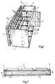
- Figure 1 illustrates schematically and in perspective a card frame and a back plane according to the invention, intended for forming a circuit card magazine.
- Figure 2 is a side view of the inventive back plane.
- Figure 1 is a perspective view of a magazine 1 according to the invention which comprises a card frame 2 and a back plane, including a printed circuit board 3.
- the card frame 2 is of conventional construction, and consists of two end plates 4 and four profiled sections 5 which connect the end plates together and are fastened at respective corners, for instance by means of screws.
- the card frame 2 is normally made of aluminium.
- the back plane of the magazine 1 instead of the conventional back plate, the back plane of the magazine 1, however, consists of a sandwich element, the nature of which will be described in more detail herebelow.
- Printed circuit cards 6 can be inserted perpendicularly to the thus formed back plane of the magazine, i.e. perpendicularly to the printed circuit board 3.
- the board 3 constitutes an electrical connecting unit between the printed circuit cards 6 and is, to this end, provided with electrical contact devices 7, whereas the printed circuit cards are provided with electrical contact devices 8 corresponding to the contact devices of the printed circuit board, as shown schematically in Figure 1.
- the cards 6 are guided in the card frame 2 by means of guide rails 9, for instance plastic rails, which extend in the card frame 2 beneath the upper and lower profiled sections 5 respectively.
- the back plane including the printed circuit board 3 will now be described with reference to Figure 2.
- the board is manufactured, e.g., of glass-fibre reinforced epoxy-resin and is provided with conductor paths, such as to enable the board to function as an electrical connecting unit for the printed circuit cards 6.
- electrical contact devices 7 are mounted on the front face of the pc-board.
- the rear side of the printed circuit board 3 is configured as a stiffening construction in the form of a sandwich element 10.
- the sandwich element 10 comprises a spacer element 11 bonded adhesively to a bottom plate 12 and secured to the circuit board.
- the spacer element comprises a layer of foamed plastic, e.g.
- the bottom plate 12 is manufactured from a material which has the same coefficient of linear expansion as the printed circuit board 3, normally a glass-fibre reinforced epoxy.
- the spacer element 11 is bonded adhesively to the printed circuit board 3, preferably subsequent to said board having been completed and tested and provided with electrical contact devices 7.
- the plane In order to enable the back plane to be mounted on the rear side of the card frame 2, the plane is provided along the edges thereof with through-passing holes 13, and the plane is screwed firmly to the rear profiled sections 5 of the card frame 2, or fastened in some other suitable manner.
- fasteners can be provided along the edges of the back plane and fastened to the profiled sections of the card frame.
- the back plane is a self-supporting, stiffening structure, as described in the foregoing, no separate mechanical reinforcements are required in the back plane of the magazine, in order to stiffen the magazine and to support the circuit board. Furthermore, because the back plane is attached to the card frame solely along the edge surfaces of the plane, the whole of the surface of the printed circuit board is available for the provison of electrical contact devices, which can thus be placed freely within the available surface area.
Landscapes
- Engineering & Computer Science (AREA)
- Microelectronics & Electronic Packaging (AREA)
- Manufacturing & Machinery (AREA)
- Mounting Of Printed Circuit Boards And The Like (AREA)
- Coupling Device And Connection With Printed Circuit (AREA)
- Combinations Of Printed Boards (AREA)
- Packaging Frangible Articles (AREA)
- Mirrors, Picture Frames, Photograph Stands, And Related Fastening Devices (AREA)
- Structures For Mounting Electric Components On Printed Circuit Boards (AREA)
- Charge And Discharge Circuits For Batteries Or The Like (AREA)
Applications Claiming Priority (2)
| Application Number | Priority Date | Filing Date | Title |
|---|---|---|---|
| SE8803634A SE500807C2 (sv) | 1988-10-12 | 1988-10-12 | Mönsterkort med kontaktdon avsett för montering i bakplan av en kortram |
| SE8803634 | 1988-10-12 |
Publications (2)
| Publication Number | Publication Date |
|---|---|
| EP0364416A1 EP0364416A1 (en) | 1990-04-18 |
| EP0364416B1 true EP0364416B1 (en) | 1994-10-12 |
Family
ID=20373605
Family Applications (1)
| Application Number | Title | Priority Date | Filing Date |
|---|---|---|---|
| EP89850267A Expired - Lifetime EP0364416B1 (en) | 1988-10-12 | 1989-08-23 | Printed circuit board for mounting in the back plane of a card frame |
Country Status (21)
| Country | Link |
|---|---|
| US (1) | US4947288A (xx) |
| EP (1) | EP0364416B1 (xx) |
| JP (1) | JP2804330B2 (xx) |
| KR (1) | KR950003245B1 (xx) |
| CN (1) | CN1015773B (xx) |
| AU (1) | AU612059B2 (xx) |
| BR (1) | BR8907117A (xx) |
| CA (1) | CA1302588C (xx) |
| DE (1) | DE68918794T2 (xx) |
| DK (1) | DK164432C (xx) |
| DZ (1) | DZ1364A1 (xx) |
| ES (1) | ES2062101T3 (xx) |
| FI (1) | FI902593A0 (xx) |
| IE (1) | IE65169B1 (xx) |
| MA (1) | MA21653A1 (xx) |
| MX (1) | MX171782B (xx) |
| NO (1) | NO175960C (xx) |
| SA (1) | SA90100074B1 (xx) |
| SE (1) | SE500807C2 (xx) |
| TR (1) | TR26727A (xx) |
| WO (1) | WO1990004321A1 (xx) |
Families Citing this family (19)
| Publication number | Priority date | Publication date | Assignee | Title |
|---|---|---|---|---|
| US5172306A (en) * | 1991-04-01 | 1992-12-15 | E-Systems, Inc. | Adaptive card mounting system |
| US5138525A (en) * | 1991-06-14 | 1992-08-11 | Dell Usa Corporation | Multi-purpose strut for digital computer chassis |
| US5214572A (en) * | 1991-08-21 | 1993-05-25 | International Business Machines Corporation | One-piece electronic cage |
| FR2689990A1 (fr) * | 1992-04-14 | 1993-10-15 | Bull Sa | Structure d'accueil pour adaptateurs de terminaux. |
| US5331517A (en) * | 1992-08-21 | 1994-07-19 | Ag Communication Systems Corporation | Retrofit card file adapter assembly |
| US5424914A (en) * | 1993-11-24 | 1995-06-13 | Unisys Corporation | Through backplane impingement cooling apparatus |
| US5459474A (en) * | 1994-03-22 | 1995-10-17 | Martin Marietta Corporation | Active array antenna radar structure |
| US5949656A (en) * | 1994-06-01 | 1999-09-07 | Davox Corporation | Electronic assembly interconnection system |
| US5982634A (en) * | 1996-11-14 | 1999-11-09 | Systran Corporation | High speed switch package provides reduced path lengths for electrical paths through the package |
| US6061249A (en) * | 1997-11-12 | 2000-05-09 | Ericsson Inc. | Sealing system and method for sealing circuit card connection sites |
| US6147863A (en) * | 1997-12-05 | 2000-11-14 | Moore; Ronald L. | Industrial computer |
| DE19952246A1 (de) * | 1998-11-04 | 2000-05-31 | Thomson Brandt Gmbh | Elektromechanisches Bauteil |
| US6320750B2 (en) * | 1998-11-24 | 2001-11-20 | Trw Inc. | Sub-modular configurable avionics |
| US6285563B1 (en) * | 1999-03-31 | 2001-09-04 | Emc Corporation | Support bracket for a printed circuit board connectable to daughter boards |
| US6549027B1 (en) | 2000-02-01 | 2003-04-15 | Sun Microsystems, Inc. | Apparatus and method for testing for compatibility between circuit boards |
| EP1391144A1 (de) * | 2001-05-29 | 2004-02-25 | Siemens Aktiengesellschaft | Baugruppenträger mit einer anschlussleiste zur aufnahme von verbinderbauteilen |
| US7251145B1 (en) * | 2004-08-18 | 2007-07-31 | Sun Microsystems, Inc. | Inject/eject mechanism for circuit boards |
| WO2015185307A1 (de) * | 2014-06-05 | 2015-12-10 | Siemens Ag Österreich | Mittel und verfahren zur befestigung einer leiterplatte |
| JP7041085B2 (ja) * | 2019-02-05 | 2022-03-23 | ファナック株式会社 | 電子装置 |
Family Cites Families (7)
| Publication number | Priority date | Publication date | Assignee | Title |
|---|---|---|---|---|
| US3810433A (en) * | 1972-08-09 | 1974-05-14 | Ncr Co | Printed circuit card guide |
| US3992686A (en) * | 1975-07-24 | 1976-11-16 | The Singer Company | Backplane transmission line system |
| JPS5384171A (en) * | 1976-12-29 | 1978-07-25 | Fujitsu Ltd | Structure for mounting printed board |
| US4131933A (en) * | 1977-04-29 | 1978-12-26 | International Business Machines Corporation | Quick disconnect card-on-board electronic package assembly |
| US4134631A (en) * | 1977-09-13 | 1979-01-16 | Amp Incorporated | Modular plug board system |
| US4511950A (en) * | 1983-06-27 | 1985-04-16 | Northern Telecom Limited | Backpanel assemblies |
| US4697858A (en) * | 1986-02-07 | 1987-10-06 | National Semiconductor Corporation | Active bus backplane |
-
1988
- 1988-10-04 TR TR89/0860A patent/TR26727A/xx unknown
- 1988-10-12 SE SE8803634A patent/SE500807C2/sv unknown
-
1989
- 1989-08-23 AU AU40784/89A patent/AU612059B2/en not_active Ceased
- 1989-08-23 ES ES89850267T patent/ES2062101T3/es not_active Expired - Lifetime
- 1989-08-23 EP EP89850267A patent/EP0364416B1/en not_active Expired - Lifetime
- 1989-08-23 BR BR898907117A patent/BR8907117A/pt not_active IP Right Cessation
- 1989-08-23 WO PCT/SE1989/000441 patent/WO1990004321A1/en active Application Filing
- 1989-08-23 DE DE68918794T patent/DE68918794T2/de not_active Expired - Fee Related
- 1989-08-23 JP JP1509031A patent/JP2804330B2/ja not_active Expired - Lifetime
- 1989-08-23 KR KR1019900701200A patent/KR950003245B1/ko not_active IP Right Cessation
- 1989-08-31 US US07/401,165 patent/US4947288A/en not_active Expired - Lifetime
- 1989-09-07 IE IE286889A patent/IE65169B1/en not_active IP Right Cessation
- 1989-09-15 CA CA000611603A patent/CA1302588C/en not_active Expired - Lifetime
- 1989-09-16 CN CN89107235A patent/CN1015773B/zh not_active Expired
- 1989-09-21 MX MX017635A patent/MX171782B/es unknown
- 1989-10-08 DZ DZ890156A patent/DZ1364A1/fr active
- 1989-10-10 MA MA21905A patent/MA21653A1/fr unknown
-
1990
- 1990-01-03 SA SA90100074A patent/SA90100074B1/ar unknown
- 1990-05-24 FI FI902593A patent/FI902593A0/fi not_active IP Right Cessation
- 1990-06-01 NO NO902454A patent/NO175960C/no unknown
- 1990-06-08 DK DK141290A patent/DK164432C/da not_active IP Right Cessation
Also Published As
| Publication number | Publication date |
|---|---|
| WO1990004321A1 (en) | 1990-04-19 |
| IE65169B1 (en) | 1995-10-04 |
| DK141290D0 (da) | 1990-06-08 |
| BR8907117A (pt) | 1991-02-05 |
| JPH03501793A (ja) | 1991-04-18 |
| SE8803634D0 (sv) | 1988-10-12 |
| DK141290A (da) | 1990-06-08 |
| CN1041860A (zh) | 1990-05-02 |
| TR26727A (tr) | 1994-07-06 |
| SA90100074B1 (ar) | 1995-12-23 |
| AU4078489A (en) | 1990-05-01 |
| FI902593A0 (fi) | 1990-05-24 |
| CA1302588C (en) | 1992-06-02 |
| NO902454L (no) | 1990-06-01 |
| SE500807C2 (sv) | 1994-09-05 |
| DE68918794D1 (de) | 1994-11-17 |
| CN1015773B (zh) | 1992-03-04 |
| IE892868L (en) | 1990-04-12 |
| DK164432B (da) | 1992-06-22 |
| DE68918794T2 (de) | 1995-02-23 |
| US4947288A (en) | 1990-08-07 |
| DZ1364A1 (fr) | 2004-09-13 |
| KR950003245B1 (ko) | 1995-04-06 |
| NO902454D0 (no) | 1990-06-01 |
| SE8803634L (sv) | 1990-04-13 |
| MX171782B (es) | 1993-11-15 |
| ES2062101T3 (es) | 1994-12-16 |
| DK164432C (da) | 1992-11-16 |
| MA21653A1 (fr) | 1990-07-01 |
| JP2804330B2 (ja) | 1998-09-24 |
| NO175960B (no) | 1994-09-26 |
| NO175960C (no) | 1995-01-04 |
| KR900702760A (ko) | 1990-12-08 |
| AU612059B2 (en) | 1991-06-27 |
| EP0364416A1 (en) | 1990-04-18 |
Similar Documents
| Publication | Publication Date | Title |
|---|---|---|
| EP0364416B1 (en) | Printed circuit board for mounting in the back plane of a card frame | |
| US5390081A (en) | Fault-tolerant power distribution system for rack-mounted hardware | |
| US5036313A (en) | Portable computer with improved assembly design | |
| EP0438012A2 (en) | Double-sided backplane assembly | |
| EP0168228B1 (en) | Display device | |
| EP0425191B1 (en) | Improved planar board support structure | |
| JPH05218670A (ja) | フレキシブル回路カード及び電子パツケージ | |
| WO2003075629A1 (en) | Adjustable sled module for mass storage devices | |
| US7137855B2 (en) | Mechanical adapter for circuitry modules | |
| US5959847A (en) | Form factor-configured channel bank card containing form factor non-conformal printed circuit board | |
| EP0889682A2 (en) | Power bus system in a tower building block system | |
| US6817881B2 (en) | Fast assembly structure module | |
| JPH0630271B2 (ja) | ケーブル・カードの組付装置 | |
| JPH07501908A (ja) | 電気工学的な装置のための装置構造 | |
| CN211509515U (zh) | 一种模块插装式pcu装置 | |
| JP4028896B2 (ja) | 組み上げシステム用の構造群 | |
| JPH02106088A (ja) | サブプリント板の取付構造 | |
| SU1765913A1 (ru) | Радиоэлектронный блок | |
| WO1993020673A1 (en) | Circuit board connections | |
| CN106255371B (zh) | 一种atr机箱的电源盒 | |
| JPS6120391A (ja) | プリント板の実装構造 | |
| JPS62219597A (ja) | プリント基板取付装置 | |
| JPH0737354Y2 (ja) | 基板の結合構造 | |
| JPH0334947Y2 (xx) | ||
| JPS58194393A (ja) | プリント配線板の接続装置 |
Legal Events
| Date | Code | Title | Description |
|---|---|---|---|
| PUAI | Public reference made under article 153(3) epc to a published international application that has entered the european phase |
Free format text: ORIGINAL CODE: 0009012 |
|
| AK | Designated contracting states |
Kind code of ref document: A1 Designated state(s): BE CH DE ES FR GB GR IT LI NL |
|
| 17P | Request for examination filed |
Effective date: 19900917 |
|
| 17Q | First examination report despatched |
Effective date: 19920928 |
|
| GRAA | (expected) grant |
Free format text: ORIGINAL CODE: 0009210 |
|
| AK | Designated contracting states |
Kind code of ref document: B1 Designated state(s): BE CH DE ES FR GB GR IT LI NL |
|
| REF | Corresponds to: |
Ref document number: 68918794 Country of ref document: DE Date of ref document: 19941117 |
|
| REG | Reference to a national code |
Ref country code: ES Ref legal event code: FG2A Ref document number: 2062101 Country of ref document: ES Kind code of ref document: T3 |
|
| ET | Fr: translation filed | ||
| ITF | It: translation for a ep patent filed | ||
| REG | Reference to a national code |
Ref country code: GR Ref legal event code: FG4A Free format text: 3013611 |
|
| PLBE | No opposition filed within time limit |
Free format text: ORIGINAL CODE: 0009261 |
|
| STAA | Information on the status of an ep patent application or granted ep patent |
Free format text: STATUS: NO OPPOSITION FILED WITHIN TIME LIMIT |
|
| 26N | No opposition filed | ||
| PGFP | Annual fee paid to national office [announced via postgrant information from national office to epo] |
Ref country code: FR Payment date: 19990802 Year of fee payment: 11 Ref country code: DE Payment date: 19990802 Year of fee payment: 11 |
|
| PGFP | Annual fee paid to national office [announced via postgrant information from national office to epo] |
Ref country code: GB Payment date: 19990803 Year of fee payment: 11 |
|
| PGFP | Annual fee paid to national office [announced via postgrant information from national office to epo] |
Ref country code: CH Payment date: 19990805 Year of fee payment: 11 |
|
| PGFP | Annual fee paid to national office [announced via postgrant information from national office to epo] |
Ref country code: NL Payment date: 19990810 Year of fee payment: 11 |
|
| PGFP | Annual fee paid to national office [announced via postgrant information from national office to epo] |
Ref country code: ES Payment date: 19990817 Year of fee payment: 11 |
|
| PGFP | Annual fee paid to national office [announced via postgrant information from national office to epo] |
Ref country code: BE Payment date: 19990819 Year of fee payment: 11 |
|
| PGFP | Annual fee paid to national office [announced via postgrant information from national office to epo] |
Ref country code: GR Payment date: 19990825 Year of fee payment: 11 |
|
| PG25 | Lapsed in a contracting state [announced via postgrant information from national office to epo] |
Ref country code: GB Free format text: LAPSE BECAUSE OF NON-PAYMENT OF DUE FEES Effective date: 20000823 |
|
| PG25 | Lapsed in a contracting state [announced via postgrant information from national office to epo] |
Ref country code: ES Free format text: LAPSE BECAUSE OF NON-PAYMENT OF DUE FEES Effective date: 20000824 |
|
| PG25 | Lapsed in a contracting state [announced via postgrant information from national office to epo] |
Ref country code: LI Free format text: LAPSE BECAUSE OF NON-PAYMENT OF DUE FEES Effective date: 20000831 Ref country code: GR Free format text: LAPSE BECAUSE OF NON-PAYMENT OF DUE FEES Effective date: 20000831 Ref country code: CH Free format text: LAPSE BECAUSE OF NON-PAYMENT OF DUE FEES Effective date: 20000831 Ref country code: BE Free format text: LAPSE BECAUSE OF NON-PAYMENT OF DUE FEES Effective date: 20000831 |
|
| BERE | Be: lapsed |
Owner name: TELEFONAKTIEBOLAGET L M ERICSSON Effective date: 20000831 |
|
| PG25 | Lapsed in a contracting state [announced via postgrant information from national office to epo] |
Ref country code: NL Free format text: LAPSE BECAUSE OF NON-PAYMENT OF DUE FEES Effective date: 20010301 |
|
| REG | Reference to a national code |
Ref country code: CH Ref legal event code: PL |
|
| GBPC | Gb: european patent ceased through non-payment of renewal fee |
Effective date: 20000823 |
|
| PG25 | Lapsed in a contracting state [announced via postgrant information from national office to epo] |
Ref country code: FR Free format text: LAPSE BECAUSE OF NON-PAYMENT OF DUE FEES Effective date: 20010430 |
|
| NLV4 | Nl: lapsed or anulled due to non-payment of the annual fee |
Effective date: 20010301 |
|
| PG25 | Lapsed in a contracting state [announced via postgrant information from national office to epo] |
Ref country code: DE Free format text: LAPSE BECAUSE OF NON-PAYMENT OF DUE FEES Effective date: 20010501 |
|
| REG | Reference to a national code |
Ref country code: FR Ref legal event code: ST |
|
| REG | Reference to a national code |
Ref country code: ES Ref legal event code: FD2A Effective date: 20010911 |
|
| PG25 | Lapsed in a contracting state [announced via postgrant information from national office to epo] |
Ref country code: IT Free format text: LAPSE BECAUSE OF NON-PAYMENT OF DUE FEES Effective date: 20050823 |