EP0361746B1 - Automatic phase controlling circuit - Google Patents
Automatic phase controlling circuit Download PDFInfo
- Publication number
- EP0361746B1 EP0361746B1 EP89309409A EP89309409A EP0361746B1 EP 0361746 B1 EP0361746 B1 EP 0361746B1 EP 89309409 A EP89309409 A EP 89309409A EP 89309409 A EP89309409 A EP 89309409A EP 0361746 B1 EP0361746 B1 EP 0361746B1
- Authority
- EP
- European Patent Office
- Prior art keywords
- phase
- signal
- variable
- difference
- detector
- Prior art date
- Legal status (The legal status is an assumption and is not a legal conclusion. Google has not performed a legal analysis and makes no representation as to the accuracy of the status listed.)
- Expired - Lifetime
Links
Images


Classifications
-
- H—ELECTRICITY
- H03—ELECTRONIC CIRCUITRY
- H03L—AUTOMATIC CONTROL, STARTING, SYNCHRONISATION, OR STABILISATION OF GENERATORS OF ELECTRONIC OSCILLATIONS OR PULSES
- H03L7/00—Automatic control of frequency or phase; Synchronisation
- H03L7/06—Automatic control of frequency or phase; Synchronisation using a reference signal applied to a frequency- or phase-locked loop
- H03L7/08—Details of the phase-locked loop
- H03L7/10—Details of the phase-locked loop for assuring initial synchronisation or for broadening the capture range
-
- H—ELECTRICITY
- H03—ELECTRONIC CIRCUITRY
- H03L—AUTOMATIC CONTROL, STARTING, SYNCHRONISATION, OR STABILISATION OF GENERATORS OF ELECTRONIC OSCILLATIONS OR PULSES
- H03L7/00—Automatic control of frequency or phase; Synchronisation
- H03L7/06—Automatic control of frequency or phase; Synchronisation using a reference signal applied to a frequency- or phase-locked loop
- H03L7/08—Details of the phase-locked loop
- H03L7/085—Details of the phase-locked loop concerning mainly the frequency- or phase-detection arrangement including the filtering or amplification of its output signal
- H03L7/087—Details of the phase-locked loop concerning mainly the frequency- or phase-detection arrangement including the filtering or amplification of its output signal using at least two phase detectors or a frequency and phase detector in the loop
Definitions
- This invention relates to an automatic phase controlling circuit operative to allow a signal variable in phase to synchronize with a reference signal.
- FIG. 1 of the drawings A typical example of the automatic phase controlling circuit is illustrated in Fig. 1 of the drawings, and comprises a low pass filter circuit (abbreviated as LPF) 1, a voltage-controlled oscillator (abbreviated as VCO) 2, and a detector (abbreviated as DET) 3.
- LPF low pass filter circuit
- VCO voltage-controlled oscillator
- DET detector
- the detector 3 is of the double-balanced type, and produces a control signal 4 the voltage level of which is variable depending upon a difference in phase between a variable-phase signal 5 and a reference signal 6 as shown in Fig. 2.
- the control signal 4 has a sawtooth waveform depending upon the difference in phase between the variable-phase signal 5 and the reference signal 6, and the variable-phase signal 5 is synchronized with the reference signal at a matching point A.
- arrows are representative of a controlling direction where the variable-phase signal 5 is delayed or advanced, and the length of each arrow is indicative of the magnitude of controlling power over the matching operation.
- the detector 3 When the variable-phase signal 5 as well as the reference signal are supplied to the detector 3, the detector 3 produces the control signal 4 in accordance with the characteristics shown in Fig. 2, and the control signal 4 is supplied through the low pass filter circuit 1 to the voltage-controlled oscillator 2 so as to match the variable-phase signal 5 with the reference signal 6. If the variable-phase signal 5 is properly synchronized with the reference signal 6 without any delay or advance, the difference in phase is zero as represented by the matching point A in Fig. 2, and, accordingly, the control signal 4 remains in zero level, thereby allowing the voltage-controlled oscillator 2 to produce the variable-phase signal 5 without any variation in phase.
- the detector 3 produces the control signal 4 in accordance with the characteristics shown in Fig. 2.
- the voltage-controlled oscillator 2 retards or advance the variable-phase signal, and, consequently, the variable-phase signal is matched in phase with the reference signal.
- the magnitude of the controlling power is not constant throughout the operation range as described hereinbefore. If the difference in phase is small at or in the vicinity of the matching point A, a small controlling power matches the variable-phase signal 5 with the reference signal 6, however, when a large difference in phase takes place, a large controlling power needs to decrease the difference.
- the sensitivity of the detector 3 is substantially constant throughout the operation range. In this situation, when the sensitivity is adjusted to a low level so as to provide a stability to the operation around the matching point, a large amount of time is consumed to match the variable-phase signal at a large difference in phase with the reference signal.
- the present invention proposes to modify the sensitivity of the detector depending upon the difference in phase from the matching point.
- an automatic phase controlling circuit for matching a frequency modified variable-phase signal with a reference signal
- a main signal loop having a main detector for producing a control signal representative of a first difference in phase between the frequency modified variable-phase signal and the reference signal, a voltage-controlled oscillator responsive to the control signal and producing a variable-phase signal, and a frequency changer operative to change the frequency of the variable-phase signal to produce the frequency modified variable-phase signal
- a sensitivity modifying unit having a phase shifter operative to change the reference signal in phase by a predetermined value to produce a modified reference signal, and an auxiliary detector for producing a sensitizing signal representative of a second difference in phase between the modified reference signal and the frequency modified variable-phase signal, in which the sensitizing signal is supplied to the main detector so that a sensitivity thereof is minimized around the first difference of about zero degree, but is increased by increasing the first difference in phase.
- an automatic phase controlling circuit largely comprises two low pass filter circuits 11 and 12, a voltage-controlled oscillator 13, a first or main detector 14, a phase shifter 15, and a second or auxiliary detector 16.
- the voltage-controlled oscillator 13 produces a variable-phase signal which is supplied in parallel to the main detectors 14 and a phase shifter 15.
- the phase shifter 15 changes the variable-phase signal 17 in phase by about 90 degrees, and the modified variable-phase signal is compared with a reference signal by the auxiliary detector 16. If a difference in phase takes place between the modified variable-phase signal 17a and the reference signal, the auxiliary detector 16 produces a sensitizing signal 19 depending upon the magnitude of the difference in phase.
- the sensitizing signal 19 is smoothed by the low pass filter circuit 12, and the smoothed sensitizing signal 19a is supplied to the main detector 14.
- Fig. 4 shows the waveform of the smoothed sensitizing signal 19a.
- the sensitivity of the detector 14 is varied by changing the smoothed sensitizing signal 19a. Namely, when the variable-phase signal 17 remains in the matching point A, the smoothed sensitizing signal has the positive maximum value which results in the minimum sensitivity of the detector 14. On the other hand, if the variable-phase signal 17 is deviated from the matching point A toward the difference in phase of 180 degrees, the smoothed sensitizing signal 19a is decreased toward the negative peak value, and the detector 14 obtains the maximum sensitivity at 180 degrees.
- the main detector 14 is responsive to the smoothed sensitizing signal 19a to modify the sensitivity thereof, and the variable-phase signal 17 is compared with the reference signal 18 by the main detector 14. If it is found that a difference in phase takes place between the variable-phase signal 17 and the reference signal 18, the main detector 14 produces a control signal 20 which is supplied through the low pass filter circuit 11 to the voltage-controlled oscillator 13.
- the control signal 20 is smoothed by the low pass filter circuit 11, and the smoothed control signal 20a varies the voltage level thereof depending upon the magnitude of the difference in phase between the variable-phase signal 17 and the reference signal 18 as shown in Fig. 5.
- the magnitude of the controlling power is dependent upon the absolute value of the voltage level of the smoothed control signal 20a, and a time period consumed for the adjustment to the reference signal 18 is decided by the combination of the sensitivity of the detector 14 and a difference from the matching point A (0 degree) or A′ (360 degrees).
- the smoothed sensitizing signal 19a increases the sensitivity of the detector from 90 degree to 270 degrees, and decreases it from 0 degrees to 90 degrees and 270 degrees to 360 degrees.
- the sensitivity of the main detector 14 is maximized at 180 degrees, which accelerates the matching operation at a large difference in phase.
- the automatic phase controlling circuit is improved on the stability without sacrifice of the quick matching operation at the large difference in phase.
- Fig. 6 illustrates a detailed circuit arrangement of an example of the detectors 14 and 16.
- the detector 14 comprises a two stage difference amplifier circuit formed by a combination of bipolar transistors Q11 to Q17 and resisters R11 to R13, and biasing nodes B11 and B12 are provided in the two stage difference amplifier circuit.
- the detector 16 comprises a two stage difference amplifier circuit formed by a combination of bipolar transistors Q1 to Q7 and resisters R1 to R3, biasing nodes B1 and B2 are also provided in the two stage difference amplifier circuit.
- the bipolar transistor Q7 of the detector 16 is supplied at the base node thereof with a constant voltage level so that the detector 16 achieves a constant gain.
- the corresponding bipolar transistor of the detector 14 is supplied at the base node thereof with the smoothed sensitizing signal 19a, and, for this reason, the gain or the sensitivity is variable depending upon the magnitude of the smoothed sensitizing signal 19a.
- the smoothed sensitizing signal as well as the smoothed control signal shown in Figs. 4 and 5 are, by way of example, assumed to be applied to an automatic phase controlling circuit incorporated in a controlling system, because the relationship between these signals should be decided in view of the total arrangement of the controlling system. This means that the signals shown in Figs. 4 and 5 are not always preferable for the circuit arrangement illustrated in Fig. 6.
- the phase shifter 15 is provided between the voltage-controlled oscillator 13 and the detector 16 in the first embodiment.
- phase shifter 15 aims at the achievement of the relationship where the sensitivity is increased by increasing the difference in phase between 90 degrees and 270 degrees or decreased by increasing the difference in phase between 0 degree and 90 degrees and between 270 degrees and 360 degrees, and, for this reason, the phase shifter may be provided in association with either detector 14 or 16.
- FIG. 7 of the drawings another automatic phase controlling circuit according to the present invention is applied to a color signal processing unit incorporated in a video tape recorder system.
- the automatic phase controlling circuit shown in Fig. 7 largely comprises two detectors 41 and 42, two low pass filter circuits 43 and 44, a voltage-controlled oscillator 45, a phase shifter 46, a crystal oscillator 47, and a frequency converter 48.
- the crystal oscillator 47 produces a reference signal 49 directly supplied to the detector 41, and the phase shifter 46 changes the reference signal 49 in phase by about 90 degrees to produce a modified reference signal 49a.
- the detectors 41 and 42 are respectively supplied with the reference signal 49 and the modified reference signal 49a as well as an input signal 50 through the frequency converter 48 which further carries out the frequency converting operation on a variable-phase signal 51 fed from the voltage-controlled oscillator 45.
- the frequency converter 48 produces an output signal 52 by eliminating a jitter component (which is given to the variable-phase signal 51) from the input signal 50
- the detector 41 is responsive to a sensitizing signal fed from the detector 42 to produce a control signal 55 fed to the voltage-controlled oscillator 45, and a predetermined relationship is established between the control signal 55 and the sensitizing signal 54 as similar to that shown in Figs. 4 and 5 by virtue of the phase shifter 46.
- the sensitizing signal 54 is shifted from the control signal 55, and, for this reason, the control signal 55 is stable around 0 degree without any sacrifice of the quick response characteristics at a large difference in phase.
- the input signal 53 is supplied to the detector 41, and the detector 41 decides whether or not any difference in phase takes place between the input signal 53 and the reference signal 49 fed from the crystal oscillator 47.
- the delayed reference signal 49a is supplied to the detector 42 and compared with the input signal 53 to produce the sensitizing signal 54.
- the detector 41 is responsive to the sensitizing signal 54 so that the sensitivity thereof is modified in accordance with the difference in phase between the delayed reference signal 49a and the input signal 50.
- the detector 41 decides whether or not any difference in phase takes place betweeen the input signal 53 and the reference signal 49, and produces the control signal in the presence of the difference in phase under the sensitivity decided by the sensitizing signal 54.
- the control signal 55 is fed to the voltage-controlled oscillator 45, and the voltage-controlled oscillator 45 is responsive to the control signal 55 to produce the variable-phase signal 51.
- the variable-phase signal 51 is subjected to the modification similar to the input signal 50, and, for this reason, the output signal 52 is stable even if the jitter component rides on the input signal 50.
- the automatic phase controlling circuit according to the present invention is advantageous over the prior art circuit in the stability around the matching point without sacrifice of the quick response characteristics at a large difference in phase by virtue of the sensitizing signal produced by the combination of the phase shifter and the auxiliary detector.
Description
- This invention relates to an automatic phase controlling circuit operative to allow a signal variable in phase to synchronize with a reference signal.
- A typical example of the automatic phase controlling circuit is illustrated in Fig. 1 of the drawings, and comprises a low pass filter circuit (abbreviated as LPF) 1, a voltage-controlled oscillator (abbreviated as VCO) 2, and a detector (abbreviated as DET) 3. The
detector 3 is of the double-balanced type, and produces a control signal 4 the voltage level of which is variable depending upon a difference in phase between a variable-phase signal 5 and areference signal 6 as shown in Fig. 2. The control signal 4 has a sawtooth waveform depending upon the difference in phase between the variable-phase signal 5 and thereference signal 6, and the variable-phase signal 5 is synchronized with the reference signal at a matching point A. However, if a difference in phase takes place between the variable-phase signal 5 and thereference signal 6, the voltage-controlledoscillator 2 advances or retards the variable-phase signal 5 with the control signal 4. In Fig. 2, arrows are representative of a controlling direction where the variable-phase signal 5 is delayed or advanced, and the length of each arrow is indicative of the magnitude of controlling power over the matching operation. - When the variable-
phase signal 5 as well as the reference signal are supplied to thedetector 3, thedetector 3 produces the control signal 4 in accordance with the characteristics shown in Fig. 2, and the control signal 4 is supplied through the lowpass filter circuit 1 to the voltage-controlledoscillator 2 so as to match the variable-phase signal 5 with thereference signal 6. If the variable-phase signal 5 is properly synchronized with thereference signal 6 without any delay or advance, the difference in phase is zero as represented by the matching point A in Fig. 2, and, accordingly, the control signal 4 remains in zero level, thereby allowing the voltage-controlledoscillator 2 to produce the variable-phase signal 5 without any variation in phase. However, if the variable-phase signal 5 is deviated in phase from the reference signal, thedetector 3 produces the control signal 4 in accordance with the characteristics shown in Fig. 2. With the control signal 4 from thedetector 3, the voltage-controlledoscillator 2 retards or advance the variable-phase signal, and, consequently, the variable-phase signal is matched in phase with the reference signal. - However, a problem is encountered in the prior art automatic phase controlling circuit in optimization of the response characteristics. In detail, the magnitude of the controlling power is not constant throughout the operation range as described hereinbefore. If the difference in phase is small at or in the vicinity of the matching point A, a small controlling power matches the variable-
phase signal 5 with thereference signal 6, however, when a large difference in phase takes place, a large controlling power needs to decrease the difference. On the other hand, the sensitivity of thedetector 3 is substantially constant throughout the operation range. In this situation, when the sensitivity is adjusted to a low level so as to provide a stability to the operation around the matching point, a large amount of time is consumed to match the variable-phase signal at a large difference in phase with the reference signal. However, if the sensitivity is large enough to rapidly match the variable-phase signal 5 at the large difference with the reference signal, the magnitude of the controlling power becomes too large to match the variable-phase signal 5 around the matching point A with thereference signal 6, and, consequently, the matching operation is deficient in the stability. Thus, there is a trade-off between the stability and the time consumed, and, for this reason, the response characteristics are hardly optimized. - It is therefore an important object of the present invention to provide an automatic phase controlling circuit which is easily optimized in the response characteristics.
- It is also another important object of the present invention to provide an automatic phase controlling circuit which has a stability around the matching point without sacrifice of quick response characteristics at a large difference in phase from the matching point.
- To accomplish the object, the present invention proposes to modify the sensitivity of the detector depending upon the difference in phase from the matching point.
- In accordance with one aspect of the present invention, there is provided an automatic phase controlling circuit for matching a variable-phase signal with a reference signal comprising a) a main signal loop having a main detector for producing a control signal representative of a first difference in phase between the variable-phase signal and the reference signal, and a voltage-controlled oscillator responsive to the control signal and producing the variable-phase signal, and b) a sensitivity modifying unit having a phase shifter operative to change the variable-phase signal in phase by a predetermined value to produce a modified variable-phase signal, and an auxiliary detector for producing a sensitizing signal representative of a second difference in phase between the modified variable-phase signal and the reference signal, in which the sensitizing signal is supplied to the main detector so that a sensitivity thereof is minimized around the first difference of about zero degree, but is increased by increasing the first difference in phase.
- In accordance with another aspect of the present invention, there is provided an automatic phase controlling circuit for matching a frequency modified variable-phase signal with a reference signal comprising a) an oscillator producing the reference signal, b) a main signal loop having a main detector for producing a control signal representative of a first difference in phase between the frequency modified variable-phase signal and the reference signal, a voltage-controlled oscillator responsive to the control signal and producing a variable-phase signal, and a frequency changer operative to change the frequency of the variable-phase signal to produce the frequency modified variable-phase signal, and c) a sensitivity modifying unit having a phase shifter operative to change the reference signal in phase by a predetermined value to produce a modified reference signal, and an auxiliary detector for producing a sensitizing signal representative of a second difference in phase between the modified reference signal and the frequency modified variable-phase signal, in which the sensitizing signal is supplied to the main detector so that a sensitivity thereof is minimized around the first difference of about zero degree, but is increased by increasing the first difference in phase.
- The features and advantages of an automatic phase controlling circuit according to the present invention will be more clearly understood from the following description taken in conjunction with the accompanying drawings in which:
- Fig. 1 is a block diagram showing the arrangement of a prior art automatic phase controlling circuit;
- Fig. 2 is a diagram showing the waveform of the control signal, in terms of the difference in phase, produced by the detector incorporated in the prior art automatic phase controlling circuit;
- Fig. 3 is a block diagram showing the arrangement of an automatic phase controlling circuit embodying the present invention;
- Fig. 4 is a diagram showing the waveform of a sensitizing signal produced in the automatic phase controlling circuit shown in Fig. 3;
- Fig. 5 is a diagram showing the waveform of a control signal produced in the automatic phase controlling circuit shown in Fig. 3;
- Fig. 6 is a circuit diagram showing the detailed arrangement of an example of the detectors incorporated in the automatic phase controlling circuit shown in Fig. 3; and
- Fig. 7 is a block diagram showing the arrangement of another automatic phase controlling circuit embodying the present invention.
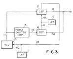
- Referring first to Fig. 3 of the drawings, an automatic phase controlling circuit according to the present invention largely comprises two low
pass filter circuits 11 and 12, a voltage-controlledoscillator 13, a first ormain detector 14, aphase shifter 15, and a second orauxiliary detector 16. The voltage-controlledoscillator 13 produces a variable-phase signal which is supplied in parallel to themain detectors 14 and aphase shifter 15. Thephase shifter 15 changes the variable-phase signal 17 in phase by about 90 degrees, and the modified variable-phase signal is compared with a reference signal by theauxiliary detector 16. If a difference in phase takes place between the modified variable-phase signal 17a and the reference signal, theauxiliary detector 16 produces asensitizing signal 19 depending upon the magnitude of the difference in phase. Thesensitizing signal 19 is smoothed by the lowpass filter circuit 12, and the smoothedsensitizing signal 19a is supplied to themain detector 14. Fig. 4 shows the waveform of the smoothedsensitizing signal 19a. The sensitivity of thedetector 14 is varied by changing the smoothedsensitizing signal 19a. Namely, when the variable-phase signal 17 remains in the matching point A, the smoothed sensitizing signal has the positive maximum value which results in the minimum sensitivity of thedetector 14. On the other hand, if the variable-phase signal 17 is deviated from the matching point A toward the difference in phase of 180 degrees, the smoothedsensitizing signal 19a is decreased toward the negative peak value, and thedetector 14 obtains the maximum sensitivity at 180 degrees. - The
main detector 14 is responsive to the smoothedsensitizing signal 19a to modify the sensitivity thereof, and the variable-phase signal 17 is compared with thereference signal 18 by themain detector 14. If it is found that a difference in phase takes place between the variable-phase signal 17 and thereference signal 18, themain detector 14 produces acontrol signal 20 which is supplied through the low pass filter circuit 11 to the voltage-controlledoscillator 13. Thecontrol signal 20 is smoothed by the low pass filter circuit 11, and the smoothed control signal 20a varies the voltage level thereof depending upon the magnitude of the difference in phase between the variable-phase signal 17 and thereference signal 18 as shown in Fig. 5. The magnitude of the controlling power is dependent upon the absolute value of the voltage level of the smoothed control signal 20a, and a time period consumed for the adjustment to thereference signal 18 is decided by the combination of the sensitivity of thedetector 14 and a difference from the matching point A (0 degree) or A′ (360 degrees). The smoothedsensitizing signal 19a increases the sensitivity of the detector from 90 degree to 270 degrees, and decreases it from 0 degrees to 90 degrees and 270 degrees to 360 degrees. Thus, the sensitivity of themain detector 14 is maximized at 180 degrees, which accelerates the matching operation at a large difference in phase. However, since the sensitivity of thedetector 14 is minimized at 0 degree and 360 degrees as described in connection with Fig. 4, the automatic phase controlling circuit is improved on the stability without sacrifice of the quick matching operation at the large difference in phase. - Fig. 6 illustrates a detailed circuit arrangement of an example of the
detectors detector 14 comprises a two stage difference amplifier circuit formed by a combination of bipolar transistors Q11 to Q17 and resisters R11 to R13, and biasing nodes B11 and B12 are provided in the two stage difference amplifier circuit. Similarly, thedetector 16 comprises a two stage difference amplifier circuit formed by a combination of bipolar transistors Q1 to Q7 and resisters R1 to R3, biasing nodes B1 and B2 are also provided in the two stage difference amplifier circuit. The bipolar transistor Q7 of thedetector 16 is supplied at the base node thereof with a constant voltage level so that thedetector 16 achieves a constant gain. However, the corresponding bipolar transistor of thedetector 14 is supplied at the base node thereof with the smoothedsensitizing signal 19a, and, for this reason, the gain or the sensitivity is variable depending upon the magnitude of the smoothedsensitizing signal 19a. The smoothed sensitizing signal as well as the smoothed control signal shown in Figs. 4 and 5 are, by way of example, assumed to be applied to an automatic phase controlling circuit incorporated in a controlling system, because the relationship between these signals should be decided in view of the total arrangement of the controlling system. This means that the signals shown in Figs. 4 and 5 are not always preferable for the circuit arrangement illustrated in Fig. 6. Furthermore, thephase shifter 15 is provided between the voltage-controlledoscillator 13 and thedetector 16 in the first embodiment. However, thephase shifter 15 aims at the achievement of the relationship where the sensitivity is increased by increasing the difference in phase between 90 degrees and 270 degrees or decreased by increasing the difference in phase between 0 degree and 90 degrees and between 270 degrees and 360 degrees, and, for this reason, the phase shifter may be provided in association with eitherdetector - Turning to Fig. 7 of the drawings, another automatic phase controlling circuit according to the present invention is applied to a color signal processing unit incorporated in a video tape recorder system. The automatic phase controlling circuit shown in Fig. 7 largely comprises two
detectors pass filter circuits 43 and 44, a voltage-controlledoscillator 45, aphase shifter 46, acrystal oscillator 47, and afrequency converter 48. Thecrystal oscillator 47 produces areference signal 49 directly supplied to thedetector 41, and thephase shifter 46 changes thereference signal 49 in phase by about 90 degrees to produce a modifiedreference signal 49a. Thedetectors reference signal 49 and the modifiedreference signal 49a as well as aninput signal 50 through thefrequency converter 48 which further carries out the frequency converting operation on a variable-phase signal 51 fed from the voltage-controlledoscillator 45. - While the
frequency converter 48 produces anoutput signal 52 by eliminating a jitter component (which is given to the variable-phase signal 51) from theinput signal 50, thedetector 41 is responsive to a sensitizing signal fed from thedetector 42 to produce acontrol signal 55 fed to the voltage-controlledoscillator 45, and a predetermined relationship is established between thecontrol signal 55 and thesensitizing signal 54 as similar to that shown in Figs. 4 and 5 by virtue of thephase shifter 46. Thus, thesensitizing signal 54 is shifted from thecontrol signal 55, and, for this reason, thecontrol signal 55 is stable around 0 degree without any sacrifice of the quick response characteristics at a large difference in phase. - In operations, the
input signal 53 is supplied to thedetector 41, and thedetector 41 decides whether or not any difference in phase takes place between theinput signal 53 and thereference signal 49 fed from thecrystal oscillator 47. On the other hand, the delayedreference signal 49a is supplied to thedetector 42 and compared with theinput signal 53 to produce the sensitizingsignal 54. Thedetector 41 is responsive to the sensitizingsignal 54 so that the sensitivity thereof is modified in accordance with the difference in phase between the delayedreference signal 49a and theinput signal 50. Thedetector 41 decides whether or not any difference in phase takes place betweeen theinput signal 53 and thereference signal 49, and produces the control signal in the presence of the difference in phase under the sensitivity decided by the sensitizingsignal 54. Thecontrol signal 55 is fed to the voltage-controlledoscillator 45, and the voltage-controlledoscillator 45 is responsive to thecontrol signal 55 to produce the variable-phase signal 51. Thus, the variable-phase signal 51 is subjected to the modification similar to theinput signal 50, and, for this reason, theoutput signal 52 is stable even if the jitter component rides on theinput signal 50. - As will be understood from the foregoing description, the automatic phase controlling circuit according to the present invention is advantageous over the prior art circuit in the stability around the matching point without sacrifice of the quick response characteristics at a large difference in phase by virtue of the sensitizing signal produced by the combination of the phase shifter and the auxiliary detector.
- Although particular embodiments of the present invention have been shown and described, it will be obvious to those skilled in the art that various changes and modifications may be made without departing from the spirit and scope of the present invention.
Claims (2)
- An automatic phase controlling circuit for matching a variable-phase signal (17) with a reference signal (18), characterized by a) a main signal loop having a main detector (14) for producing a control signal (20) representative of a first difference in phase between said variable-phase signal and said reference signal, and a voltage-controlled oscillator (13) responsive to said control signal and producing said variable-phase signal, and b) a sensitivity modifying unit having a phase shifter (15) operative to change said variable-phase signal in phase by a predetermined value to produce a modified variable-phase signal (17a), and an auxiliary detector (16) for producing a sensitizing signal (19) representative of a second difference in phase between the modified variable-phase signal and said reference signal, and in that said sensitizing signal is supplied to said main detector so that a sensitivity thereof is minimized around the first difference of about zero degree, but is increased by increasing the first difference in phase.
- An automatic phase controlling circuit for matching a frequency modified variable-phase signal (53) with a reference signal (49), characterized by a) an oscillator (47) producing said reference signal, b) a main signal loop having a main detector (41) for producing a control signal (55) representative of a first difference in phase between said frequency modified variable-phase signal and said reference signal, a voltage-controlled oscillator (45) responsive to said control signal and producing a variable-phase signal (51), and a frequency changer (48) operative to change the frequency of the variable-phase signal to produce said frequency modified variable-phase signal, and c) a sensitivity modifying unit having a phase shifter (46) operative to change said reference signal in phase by a predetermined value to produce a modified reference signal (49a), and an auxiliary detector (42) for producing a sensitizing signal (54) representative of a second difference in phase between the modified reference signal and said frequency modified variable-phase signal, and in that said sensitizing signal is supplied to said main detector so that a sensitivity thereof is minimized around the first difference of about zero degree, but is increased by increasing the first difference in phase.
Applications Claiming Priority (2)
| Application Number | Priority Date | Filing Date | Title |
|---|---|---|---|
| JP63241405A JP2770342B2 (en) | 1988-09-26 | 1988-09-26 | Automatic phase control circuit |
| JP241405/88 | 1988-09-26 |
Publications (3)
| Publication Number | Publication Date |
|---|---|
| EP0361746A2 EP0361746A2 (en) | 1990-04-04 |
| EP0361746A3 EP0361746A3 (en) | 1990-06-20 |
| EP0361746B1 true EP0361746B1 (en) | 1994-04-13 |
Family
ID=17073795
Family Applications (1)
| Application Number | Title | Priority Date | Filing Date |
|---|---|---|---|
| EP89309409A Expired - Lifetime EP0361746B1 (en) | 1988-09-26 | 1989-09-15 | Automatic phase controlling circuit |
Country Status (4)
| Country | Link |
|---|---|
| US (1) | US5051702A (en) |
| EP (1) | EP0361746B1 (en) |
| JP (1) | JP2770342B2 (en) |
| DE (1) | DE68914564T2 (en) |
Families Citing this family (4)
| Publication number | Priority date | Publication date | Assignee | Title |
|---|---|---|---|---|
| US5084681A (en) * | 1990-08-03 | 1992-01-28 | Hewlett-Packard Company | Digital synthesizer with phase memory |
| US5408192A (en) * | 1993-10-12 | 1995-04-18 | International Business Machines Corporation | Monolithic broadband phase shifting circuit for analog data signals |
| JP2871560B2 (en) * | 1995-11-21 | 1999-03-17 | 日本電気株式会社 | π / 2 phase shifter |
| US6208181B1 (en) * | 1998-01-14 | 2001-03-27 | Intel Corporation | Self-compensating phase detector |
Family Cites Families (9)
| Publication number | Priority date | Publication date | Assignee | Title |
|---|---|---|---|---|
| US3465258A (en) * | 1966-12-21 | 1969-09-02 | North American Rockwell | Phase lock demodulator |
| US3621405A (en) * | 1968-05-28 | 1971-11-16 | Itek Corp | Sinusoidal converter |
| US3588734A (en) * | 1969-04-21 | 1971-06-28 | Westinghouse Electric Corp | Nonlinear phase detector |
| US3952261A (en) * | 1972-11-06 | 1976-04-20 | Fujitsu Ltd. | Signal detection circuit |
| US3787775A (en) * | 1973-03-28 | 1974-01-22 | Trw Inc | Phase correction circuit |
| DE2853890C2 (en) * | 1978-12-14 | 1986-03-13 | ANT Nachrichtentechnik GmbH, 7150 Backnang | Method for demodulating phase, amplitude or frequency modulated signals with the aid of a phase-locked loop |
| JPS5848501B2 (en) * | 1979-06-26 | 1983-10-28 | 触媒化成工業株式会社 | Method for manufacturing low soda alumina compacts with low bulk density and high crushing strength |
| JPS5651128A (en) * | 1979-10-04 | 1981-05-08 | Sony Corp | Pll |
| JPS62177129U (en) * | 1986-04-29 | 1987-11-10 |
-
1988
- 1988-09-26 JP JP63241405A patent/JP2770342B2/en not_active Expired - Lifetime
-
1989
- 1989-09-12 US US07/406,359 patent/US5051702A/en not_active Expired - Fee Related
- 1989-09-15 EP EP89309409A patent/EP0361746B1/en not_active Expired - Lifetime
- 1989-09-15 DE DE68914564T patent/DE68914564T2/en not_active Expired - Lifetime
Also Published As
| Publication number | Publication date |
|---|---|
| DE68914564T2 (en) | 1994-07-21 |
| EP0361746A2 (en) | 1990-04-04 |
| JPH0287822A (en) | 1990-03-28 |
| EP0361746A3 (en) | 1990-06-20 |
| DE68914564D1 (en) | 1994-05-19 |
| JP2770342B2 (en) | 1998-07-02 |
| US5051702A (en) | 1991-09-24 |
Similar Documents
| Publication | Publication Date | Title |
|---|---|---|
| EP0423941A3 (en) | Variable frequency signal generator | |
| JPS62231548A (en) | Frequency modulated signal receiver | |
| EP0361746B1 (en) | Automatic phase controlling circuit | |
| EP0557867B1 (en) | Double phase locked loop circuit | |
| US5239367A (en) | Signal discriminating circuit and active filter using same | |
| JPH09223960A (en) | Phase synchronizer | |
| US5097219A (en) | Pll for controlling frequency deviation of a variable frequency oscillator | |
| US20040036540A1 (en) | Controlling an oscillator or a phase-delay device in a phase-control circuit | |
| US5347240A (en) | Circuit and method for automatically controlling the carrier frequency of a video recording device | |
| JP3209211B2 (en) | Phase locked loop | |
| JPH0156580B2 (en) | ||
| JPS5846586Y2 (en) | Circuit with phase locked loop | |
| JP2732541B2 (en) | Signal oscillator | |
| KR100213251B1 (en) | Apparatus for adjusting frequency of voltage controlled oscillator automatically | |
| JPH0440104A (en) | Phase locked loop circuit of ultra high frequency diode oscillator | |
| JPH1079666A (en) | Phase locked loop oscillation circuit | |
| JP2721927B2 (en) | PLL circuit | |
| JPH04344713A (en) | Phase synchronizing circuit | |
| KR100218524B1 (en) | Filter auto-control system | |
| JPH05284015A (en) | Phase locked loop circuit | |
| US4918407A (en) | Oscillation circuit | |
| JP2000188544A (en) | Phase locked loop circuit | |
| JPH02148915A (en) | Phase synchronizing oscillation circuit | |
| JPH07240684A (en) | Phase locked loop circuit | |
| KR19980029355A (en) | Carrier Frequency Regulator Using Crystal Oscillator and Voltage Controlled Oscillator |
Legal Events
| Date | Code | Title | Description |
|---|---|---|---|
| PUAI | Public reference made under article 153(3) epc to a published international application that has entered the european phase |
Free format text: ORIGINAL CODE: 0009012 |
|
| 17P | Request for examination filed |
Effective date: 19890923 |
|
| AK | Designated contracting states |
Kind code of ref document: A2 Designated state(s): DE FR GB NL |
|
| PUAL | Search report despatched |
Free format text: ORIGINAL CODE: 0009013 |
|
| AK | Designated contracting states |
Kind code of ref document: A3 Designated state(s): DE FR GB NL |
|
| 17Q | First examination report despatched |
Effective date: 19930624 |
|
| GRAA | (expected) grant |
Free format text: ORIGINAL CODE: 0009210 |
|
| AK | Designated contracting states |
Kind code of ref document: B1 Designated state(s): DE FR GB NL |
|
| PG25 | Lapsed in a contracting state [announced via postgrant information from national office to epo] |
Ref country code: NL Effective date: 19940413 Ref country code: FR Effective date: 19940413 |
|
| REF | Corresponds to: |
Ref document number: 68914564 Country of ref document: DE Date of ref document: 19940519 |
|
| EN | Fr: translation not filed | ||
| NLV1 | Nl: lapsed or annulled due to failure to fulfill the requirements of art. 29p and 29m of the patents act | ||
| PLBE | No opposition filed within time limit |
Free format text: ORIGINAL CODE: 0009261 |
|
| STAA | Information on the status of an ep patent application or granted ep patent |
Free format text: STATUS: NO OPPOSITION FILED WITHIN TIME LIMIT |
|
| 26N | No opposition filed | ||
| PGFP | Annual fee paid to national office [announced via postgrant information from national office to epo] |
Ref country code: DE Payment date: 20000911 Year of fee payment: 12 |
|
| PGFP | Annual fee paid to national office [announced via postgrant information from national office to epo] |
Ref country code: GB Payment date: 20000913 Year of fee payment: 12 |
|
| PG25 | Lapsed in a contracting state [announced via postgrant information from national office to epo] |
Ref country code: GB Free format text: LAPSE BECAUSE OF NON-PAYMENT OF DUE FEES Effective date: 20010915 |
|
| REG | Reference to a national code |
Ref country code: GB Ref legal event code: IF02 |
|
| PG25 | Lapsed in a contracting state [announced via postgrant information from national office to epo] |
Ref country code: DE Free format text: LAPSE BECAUSE OF NON-PAYMENT OF DUE FEES Effective date: 20020501 |
|
| GBPC | Gb: european patent ceased through non-payment of renewal fee |
Effective date: 20010915 |