EP0356571A1 - Steuerschaltung für EEPROM - Google Patents
Steuerschaltung für EEPROM Download PDFInfo
- Publication number
- EP0356571A1 EP0356571A1 EP88114382A EP88114382A EP0356571A1 EP 0356571 A1 EP0356571 A1 EP 0356571A1 EP 88114382 A EP88114382 A EP 88114382A EP 88114382 A EP88114382 A EP 88114382A EP 0356571 A1 EP0356571 A1 EP 0356571A1
- Authority
- EP
- European Patent Office
- Prior art keywords
- circuit
- high voltage
- pulse
- voltage
- eeprom
- Prior art date
- Legal status (The legal status is an assumption and is not a legal conclusion. Google has not performed a legal analysis and makes no representation as to the accuracy of the status listed.)
- Granted
Links
- 238000007493 shaping process Methods 0.000 claims abstract description 12
- 230000000630 rising effect Effects 0.000 claims abstract description 11
- 230000010355 oscillation Effects 0.000 claims abstract description 6
- 238000010586 diagram Methods 0.000 description 10
- 230000006870 function Effects 0.000 description 7
- 239000004065 semiconductor Substances 0.000 description 2
- XUIMIQQOPSSXEZ-UHFFFAOYSA-N Silicon Chemical compound [Si] XUIMIQQOPSSXEZ-UHFFFAOYSA-N 0.000 description 1
- 239000003990 capacitor Substances 0.000 description 1
- 238000006243 chemical reaction Methods 0.000 description 1
- 238000013500 data storage Methods 0.000 description 1
- 238000000034 method Methods 0.000 description 1
- 229910052710 silicon Inorganic materials 0.000 description 1
- 239000010703 silicon Substances 0.000 description 1
Images




Classifications
-
- G—PHYSICS
- G11—INFORMATION STORAGE
- G11C—STATIC STORES
- G11C16/00—Erasable programmable read-only memories
- G11C16/02—Erasable programmable read-only memories electrically programmable
- G11C16/06—Auxiliary circuits, e.g. for writing into memory
- G11C16/30—Power supply circuits
Definitions
- This invention relates to a control circuit for an EEPROM (Electrically Erasable Programmable Read Only Memory), more particularly to a control circuit generating a high voltage pulse enabling a rewrite function of EEPROM data with low voltage and low power consumption.
- EEPROM Electrically Erasable Programmable Read Only Memory
- EEPROMs available not only for use as a single unit but for constituting an one-chip microcomputer in combination with a microprocessor, which can be constructed as a CMOS structure.
- a semiconductor integrated circuit in which the EEPROM is incorporated has a wide variety of applications such as replacement of a mechanical switch, an IC card having function which stores and adjusts operational procedures of a calculator or stores and refreshes data. (Ex. See NIKKEI ELECTRONICS, Oct. 21, 1985 P. 127)
- Fig. 6 shows a block diagram of a control circuit for EEPROM with 5V single power supply operation generating a high voltage pulse for data write/erase/read.
- the power supply voltage of 5V is applied to a clock pulse generation circuit 1 so that a clock pulse train having a frequency of 5-10MH z and a peak wave value 5V can be achieved.
- a step-up voltage of 23-25V can be output.
- Fig. 7 shown an example of the conventional voltage booster circuit having 10-13 booster stages which are adequate for obtaining a step-up voltage of 20-25V from a source voltage of 5V.
- the high voltage of 20-25V generated by the booster circuit 2 is applied to a regulator circuit 3 which stabilizes the high voltage to a constant level voltage.
- Fig. 8(A) shows a concrete circuit of the regulator circuit, the output voltage of which is 18-20V in direct current (D.C.).
- a wave shaping circuit 4 generates a high voltage pulse which is necessary to write/erase data of cells of the EEPROM.
- the high voltage pulse requires a peak wave value of 18-20V and a constant rising rate, for example, 16V/ms.
- FIG. 8(B) One embodiment of the concrete wave shaping circuit is shown in Fig. 8(B).
- a high voltage switch circuit 5 to switch the high voltage pulse generated by the wave shaping circuit 4 to a writing direction or to an erasing direction, interchangeably.
- Fig. 8(C) shows a concrete circuit of the high voltage switch circuit 5.
- the high voltage pulse is switched interchangeably by the high voltage switch circuit 5 such a manner that the high voltage pulse is applied to a drain electrode of the memory cell in accordance with a writing signal W in case of writing, whereas it is applied to a gate electrode of the memory cell in accordance with an erasing signal E on erasing.
- a memory cell 6 is constituted by being arrayed a plurality of FETs with a double layer silicon gate structure comprising a source electrode, a drain electrode, a floating gate and a gate electrode.
- FIG. 9 One embodiment of the concrete circuit is shown in Fig. 9.
- the writing function to the memory cell 6 is performed such that the high voltage pulse is applied between the drain and the gate with the gate electrode being fixed to zero volt.
- the erasing cycle is performed such that the high voltage pulse is applied between the gate and the drain with the drain electrode being fixed to zero volt.
- An object of the present invention is to provide a control circuit for an EEPROM which enables writing and erasing data to the EEPROM with low voltage of an approximate 1.5V and low current less than a few hundred uA.
- a control circuit generating a write/erase high voltage pulse for an EEPROM which comprises a low frequency clock pulse oscillation circuit, a voltage booster circuit having at least 19 FET booster stages and a high voltage shaping switch circuit having an exponential rising pulse edge driven by the clock pulse.
- a low current consumption can be achieved by driving the control circuit by the low frequency clock pulse of an approximate 30KH z , and a high voltage necessary for writing to the EEPROM can be achieved from a low voltage with high conversion efficiency by employing the voltage booster circuit having at least 19 FET booster stages.
- the high voltage switch circuit having an exponential rising pulse edge requires no special wave shaping circuit so that a simplified and low voltage operated circuit can be achieved.
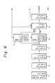
- the control circuit for the EEPROM comprises a low frequency pulse oscillation circuit 11, a voltage booster circuit 12, and a high voltage shaping switch circuit 13.
- the low frequency clock pulse oscillation circuit 11 is an oscillator generating an approximate 30KH z frequency driven by low voltage and low current.
- the adequate frequency range for the clock pulse lies between 20KH z and 100KH z .
- the present embodiment shows an oscillator operating with a 1.5V source voltage and a few uA consumption current.
- the voltage booster circuit 12 is a booster circuit with low power consumption which operates with low power source driven by the oscillation circuit 11.
- the present invention employs at least 19 stages, particularly in the present embodiment 24 stages, to operate with low power voltage of an approximate 1.5V.
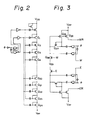
- Fig. 2 shows a circuit diagram of the voltage booster circuit in accordance with the present embodiment.
- Transistors Q1 - Q24 constitute the booster stages, each of which is constituted by zero threshold FETs.
- the zero threshold FET is an FET where the threshold voltage is controlled to be nearly zero volt (approximately 0 ⁇ 0.4V).
- Utilization of the zero threshold voltage FET in the booster stage enables to elevate voltage efficiently without voltage loss.
- an approximate 20V high voltage necessary for writing and erasing of the EEPROM can be obtained as an output voltage V pp about 20ms later after the clock is supplied under conditions of the power source voltage V DD being 1.5V, the booster stage being 24 and the clock frequency being 30KH z .
- the voltage booster circuit according to the present invention employs at least 19 stage zero threshold FETs and is driven by the low voltage power source V DD having an approximate 1.5V and the slow clock having an approximate 30KH z so that the output voltage V pp having an approximate 20V which is adequete for writing and erasing of the cell of the EEPROM can be obtained.
- a regulator circuit which is used in the conventional circuit is not necessarily required because the voltage booster circuit has the same function.
- the high voltage shaping switch circuit 13 is a circuit which forms a high voltage pulse needed for data writing and erasing of the memory cell 14 by using the approximate 20V achieved by the booster circuit 12.
- Fig. 3 shows an embodiment of the circuit.
- a high voltage WR for writing can be formed from the D. C. voltage V pp by the functions of transistors Q25, Q26 and Q27 and two capasitors.
- This high voltage pulse is of an exponential type which has a 1-5 ms rising edge due to the function of transistor and capacitor of 1-2pF when driven by the clock pulse of an approximate 30KH z .
- Fig. 5 shows a wave form chart illustrating the rising edge of the pulse.
- the exponential type pulse is particularly suitable with an approximate 1 ms rising edge.
- the memory cell 14 itself is the same type as the conventional one arrayed by FETs for data storage having source-drain electrodes, a floating gate and a normal gate.
- the positive electric charges injected in writing cycle are erased and further negative charges are accumulated.
- a read-out signal RD is set to be "1".
- the memory cell FET 601 becomes conductive between the source and the drain so that the drain current flows through the FETs 610, 601 and 606.
- an inverter 614 and an FET 613 read out date "1".
- the memroy cell FET 601 does not become conductive so that the drain current does not flow through the FETs 610, 601 and 606.
Landscapes
- Read Only Memory (AREA)
Priority Applications (2)
| Application Number | Priority Date | Filing Date | Title |
|---|---|---|---|
| EP19880114382 EP0356571B1 (de) | 1988-09-02 | 1988-09-02 | Steuerschaltung für EEPROM |
| DE8888114382T DE3868511D1 (de) | 1988-09-02 | 1988-09-02 | Steuerschaltung fuer eeprom. |
Applications Claiming Priority (1)
| Application Number | Priority Date | Filing Date | Title |
|---|---|---|---|
| EP19880114382 EP0356571B1 (de) | 1988-09-02 | 1988-09-02 | Steuerschaltung für EEPROM |
Publications (2)
| Publication Number | Publication Date |
|---|---|
| EP0356571A1 true EP0356571A1 (de) | 1990-03-07 |
| EP0356571B1 EP0356571B1 (de) | 1992-02-19 |
Family
ID=8199266
Family Applications (1)
| Application Number | Title | Priority Date | Filing Date |
|---|---|---|---|
| EP19880114382 Expired EP0356571B1 (de) | 1988-09-02 | 1988-09-02 | Steuerschaltung für EEPROM |
Country Status (2)
| Country | Link |
|---|---|
| EP (1) | EP0356571B1 (de) |
| DE (1) | DE3868511D1 (de) |
Cited By (1)
| Publication number | Priority date | Publication date | Assignee | Title |
|---|---|---|---|---|
| US4977543A (en) * | 1987-08-31 | 1990-12-11 | Oki Electric Industry Co., Ltd. | Control circuit for EEPROM |
Citations (2)
| Publication number | Priority date | Publication date | Assignee | Title |
|---|---|---|---|---|
| US4326134A (en) * | 1979-08-31 | 1982-04-20 | Xicor, Inc. | Integrated rise-time regulated voltage generator systems |
| US4488060A (en) * | 1979-01-24 | 1984-12-11 | Xicor, Inc. | High voltage ramp rate control systems |
-
1988
- 1988-09-02 DE DE8888114382T patent/DE3868511D1/de not_active Expired - Fee Related
- 1988-09-02 EP EP19880114382 patent/EP0356571B1/de not_active Expired
Patent Citations (2)
| Publication number | Priority date | Publication date | Assignee | Title |
|---|---|---|---|---|
| US4488060A (en) * | 1979-01-24 | 1984-12-11 | Xicor, Inc. | High voltage ramp rate control systems |
| US4326134A (en) * | 1979-08-31 | 1982-04-20 | Xicor, Inc. | Integrated rise-time regulated voltage generator systems |
Non-Patent Citations (2)
| Title |
|---|
| ELECTRONICS & COMMUNICATIONS IN JAPAN, vol. 67-C, no. 5, May 1984, pages 91-99, Scripta Publishing Co., Silver Spring, Maryland, US; Y. YATSUDA et al.: "A byte erasable 5V-only 64 Kbit EEPROM" * |
| IEEE JOURNAL OF SOLID-STATE CIRCUITS, vol. SC-18, no. 5, October 1983, pages 532-538, IEEE, New York, US; D.H. OTO et al.: "High-voltage regulation and process considerations for high-density 5 V-only E2PROM's" * |
Cited By (1)
| Publication number | Priority date | Publication date | Assignee | Title |
|---|---|---|---|---|
| US4977543A (en) * | 1987-08-31 | 1990-12-11 | Oki Electric Industry Co., Ltd. | Control circuit for EEPROM |
Also Published As
| Publication number | Publication date |
|---|---|
| DE3868511D1 (de) | 1992-03-26 |
| EP0356571B1 (de) | 1992-02-19 |
Similar Documents
| Publication | Publication Date | Title |
|---|---|---|
| US6188293B1 (en) | Low power oscillation circuit and non-volatile semiconductor memory having ring oscillator | |
| US6356469B1 (en) | Low voltage charge pump employing optimized clock amplitudes | |
| US5553030A (en) | Method and apparatus for controlling the output voltage provided by a charge pump circuit | |
| JP4094104B2 (ja) | 半導体集積回路装置および記憶装置 | |
| EP0717874A1 (de) | Ladungspumpendes flash-eeprom | |
| US4907202A (en) | Control circuit for EEPROM | |
| KR20000062549A (ko) | 저전압 전원에 대응한 승압 회로 | |
| EP0376065B1 (de) | Integrierte Halbleiterspeicherschaltung | |
| US20020041503A1 (en) | Low voltage charge pump employing distributed charge boosting | |
| US5105384A (en) | Low current semiconductor memory device | |
| CN110197694A (zh) | 位准移位器与半导体装置 | |
| KR0136378B1 (ko) | 반도체 기억장치 | |
| EP0807936A3 (de) | Für die Löschspannungsversorgung einer Flash-Speicherzelle geeignete nichtflüchtige Halbleiterspeichernanordnung | |
| US5101381A (en) | Control circuit for EEPROM | |
| CN102750981B (zh) | 半导体存储器的内部电源电压生成电路及生成方法 | |
| EP0288075B1 (de) | Zusatz-Boosterschaltung zum Anheben der Ausgangsspannung einer Haupt-Boosterspannung | |
| EP0356571A1 (de) | Steuerschaltung für EEPROM | |
| US6414882B1 (en) | Low voltage charge pump apparatus and method | |
| US4831589A (en) | EEPROM programming switch operable at low VCC | |
| JPH06302197A (ja) | シリアル情報処理するためのmosメモリ | |
| JP2006185530A (ja) | 不揮発性半導体メモリ装置 | |
| JP3553508B2 (ja) | 発信回路 | |
| JPH0418709B2 (de) | ||
| CN111522428B (zh) | 微控制器内嵌入闪存电源调节方法 | |
| JP2562395B2 (ja) | 電源回路 |
Legal Events
| Date | Code | Title | Description |
|---|---|---|---|
| PUAI | Public reference made under article 153(3) epc to a published international application that has entered the european phase |
Free format text: ORIGINAL CODE: 0009012 |
|
| 17P | Request for examination filed |
Effective date: 19890922 |
|
| AK | Designated contracting states |
Kind code of ref document: A1 Designated state(s): DE FR GB |
|
| 17Q | First examination report despatched |
Effective date: 19900508 |
|
| GRAA | (expected) grant |
Free format text: ORIGINAL CODE: 0009210 |
|
| AK | Designated contracting states |
Kind code of ref document: B1 Designated state(s): DE FR GB |
|
| REF | Corresponds to: |
Ref document number: 3868511 Country of ref document: DE Date of ref document: 19920326 |
|
| ET | Fr: translation filed | ||
| PLBE | No opposition filed within time limit |
Free format text: ORIGINAL CODE: 0009261 |
|
| STAA | Information on the status of an ep patent application or granted ep patent |
Free format text: STATUS: NO OPPOSITION FILED WITHIN TIME LIMIT |
|
| 26N | No opposition filed | ||
| PGFP | Annual fee paid to national office [announced via postgrant information from national office to epo] |
Ref country code: GB Payment date: 19980824 Year of fee payment: 11 |
|
| PGFP | Annual fee paid to national office [announced via postgrant information from national office to epo] |
Ref country code: FR Payment date: 19980909 Year of fee payment: 11 |
|
| PGFP | Annual fee paid to national office [announced via postgrant information from national office to epo] |
Ref country code: DE Payment date: 19980914 Year of fee payment: 11 |
|
| PG25 | Lapsed in a contracting state [announced via postgrant information from national office to epo] |
Ref country code: GB Free format text: LAPSE BECAUSE OF NON-PAYMENT OF DUE FEES Effective date: 19990902 |
|
| GBPC | Gb: european patent ceased through non-payment of renewal fee |
Effective date: 19990902 |
|
| PG25 | Lapsed in a contracting state [announced via postgrant information from national office to epo] |
Ref country code: FR Free format text: LAPSE BECAUSE OF NON-PAYMENT OF DUE FEES Effective date: 20000531 |
|
| PG25 | Lapsed in a contracting state [announced via postgrant information from national office to epo] |
Ref country code: DE Free format text: LAPSE BECAUSE OF NON-PAYMENT OF DUE FEES Effective date: 20000701 |
|
| REG | Reference to a national code |
Ref country code: FR Ref legal event code: ST |