EP0352937B1 - Datenfehler-Detektion und -Korrektur - Google Patents
Datenfehler-Detektion und -Korrektur Download PDFInfo
- Publication number
- EP0352937B1 EP0352937B1 EP89307076A EP89307076A EP0352937B1 EP 0352937 B1 EP0352937 B1 EP 0352937B1 EP 89307076 A EP89307076 A EP 89307076A EP 89307076 A EP89307076 A EP 89307076A EP 0352937 B1 EP0352937 B1 EP 0352937B1
- Authority
- EP
- European Patent Office
- Prior art keywords
- trinary
- output
- trit
- input
- data
- Prior art date
- Legal status (The legal status is an assumption and is not a legal conclusion. Google has not performed a legal analysis and makes no representation as to the accuracy of the status listed.)
- Expired - Lifetime
Links
Images


Classifications
-
- H—ELECTRICITY
- H03—ELECTRONIC CIRCUITRY
- H03M—CODING; DECODING; CODE CONVERSION IN GENERAL
- H03M13/00—Coding, decoding or code conversion, for error detection or error correction; Coding theory basic assumptions; Coding bounds; Error probability evaluation methods; Channel models; Simulation or testing of codes
-
- H—ELECTRICITY
- H03—ELECTRONIC CIRCUITRY
- H03M—CODING; DECODING; CODE CONVERSION IN GENERAL
- H03M5/00—Conversion of the form of the representation of individual digits
- H03M5/02—Conversion to or from representation by pulses
- H03M5/16—Conversion to or from representation by pulses the pulses having three levels
-
- H—ELECTRICITY
- H03—ELECTRONIC CIRCUITRY
- H03M—CODING; DECODING; CODE CONVERSION IN GENERAL
- H03M5/00—Conversion of the form of the representation of individual digits
- H03M5/02—Conversion to or from representation by pulses
- H03M5/20—Conversion to or from representation by pulses the pulses having more than three levels
-
- G—PHYSICS
- G06—COMPUTING; CALCULATING OR COUNTING
- G06F—ELECTRIC DIGITAL DATA PROCESSING
- G06F11/00—Error detection; Error correction; Monitoring
- G06F11/07—Responding to the occurrence of a fault, e.g. fault tolerance
- G06F11/08—Error detection or correction by redundancy in data representation, e.g. by using checking codes
- G06F11/10—Adding special bits or symbols to the coded information, e.g. parity check, casting out 9's or 11's
- G06F11/1008—Adding special bits or symbols to the coded information, e.g. parity check, casting out 9's or 11's in individual solid state devices
- G06F11/1072—Adding special bits or symbols to the coded information, e.g. parity check, casting out 9's or 11's in individual solid state devices in multilevel memories
Definitions
- the present invention relates to a data error detection and correction in multi-level logic and is further described with reference to an embodiment thereof which operates in the trinary mode of 0, 1, and 2.
- Prior art systems which operate in three-level logic have one of the voltages at a negative level, i.e., voltage levels of -1, 0, +1, which are respectively referred to as data quantities of 0, 1, 2.
- voltage levels of -1, 0, +1 which are respectively referred to as data quantities of 0, 1, 2.
- No prior art systems are known to operate with all voltages at single polarity voltage levels to generate data logic of 0, 1, 2 nor are there any known three-level systems which include error detection or correction.
- trinary three-level logic offers a variety of advantages over the familiar binary two-level logic with two of these advantages being a reduction in components and increased data capacity.
- trinary data can be depended upon for processing information, there must be an error detection and correction function performed on the data during movement or storage of the data.
- error detection and correction function performed on the data during movement or storage of the data.
- the use of trinary data is sparse in the prior art. There are no known techniques for trinary data error handling.
- Trinary data (described herein as the three logic levels, 0, 1, 2) has been used to transmit data between binary logic units (see U. S. 4,631,428 assigned to International Business Machines Corporation). However, this type of trinary data has not been used to perform logic functions which require error checking. As trinary data and logic become more widely used in data processing as a technique to increase capacity, so will the need to perform error checking and correction.
- U. S. 4,523,314 discloses an error indicating system for use with a binary error detection and correction system.
- the system diagram in Fig. 1 includes the basic functions needed to perform an error detection and correction. These are: reading in and storing data while generating first check bits; reading out the stored data and generating second check bits; using the syndrome bits to indicate errors and to signal error correction circuitry.
- the problems encountered in using the system disclosed in U.S. 4,523,314 or a similar binary system in the trinary mode of the invention are numerous.
- the basic problems are the storing of trinary data; the generation of a check trit; the generation of syndrome elements; the error decoder and error detection procedure; and the error correction function.
- the known techniques for performing these functions in binary are not applicable to a trinary system without making unique and basic changes to the known prior art.
- Known binary storage devices such as latches do not exist for trinary.
- Binary check bit generators cannot be used as is or altered to perform the generation of trinary check trits.
- the binary syndrome generators are AND logic groups and do not function to generate three-level syndrome elements. Error detection and correction techniques in binary are based on the principle of errors have changed data from 0 to 1 or 1 to 0.
- U. S. 4,523,314 uses adders and carry detectors since binary loss or gain will be detected by loss or gain of carry.
- Trinary error correction techniques have to determine the level of data error, i.e. 0, or 1, or 2. None of the binary logic or techniques including the use of adders and carry detectors are therefore applicable.
- U.S. 3,755,779; 3,896,416 and 4,631,725 are typical binary error correction systems which generate check bits and syndrome elements to perform error correction. Comparison of syndrome generation techniques show the use of modulo-two and summations to generate the syndrome bits. The binary one-zero summations are relatively simple from a logic standpoint, however, this approach could not be applied to trinary.
- a method for generating a trinary check trit of trinary logic level 0, or 1, or 2 for first and second input trits including: applying the first input trit to a first input of a check trit generator; setting the trinary logic level at each of a first circuit point and a second circuit point in the trit generator in dependence on the first input trit via a first group of trinary logic devices of the trit generator connected to the first input; applying the second input trit to a second input of the trit generator; selecting the trinary logic level at one of the first circuit point, the second circuit point, and the first input in response to the second input trit via a second group of trinary logic devices of the check trit generator connected to the second input; setting the trinary logic level of an output line in dependence on the selected trinary logic level; whereby the trinary logic level applied to the output line is dependent upon the combination of logic levels applies to the first and second input trits.
- the present invention equally provides a trinary check trit generator for generating a trinary check logic level 0, or 1, or 2 for first and second input trits, the generator comprising: a first input for receiving a first input trit; a first group of trinary logic devices connected to the first input for setting the trinary logic at each of a first circuit point and a second circuit point in dependence on the first input trit; a second input for receiving a second input trit; a second group of trinary logic devices connected to the second input for selecting the trinary logic level at one of the first circuit point, the second circuit point and the first input in response to the second input trit; an output line; and, means for setting the trinary logic level of the output line in dependence on the selected trinary logic level; whereby the trinary logic level applied to the output line is dependent upon the combination of logic levels applied to the first and second inputs.
- One such arrangement disclosed hereinafter uses a trit of trinary data (which is at the 0, or 1, or 2 level compared to a bit of binary data at the 0, or 1 logic level).
- a trit of trinary data which is at the 0, or 1, or 2 level compared to a bit of binary data at the 0, or 1 logic level.
- a first series of check trits are generated which are unique for each particular group of trits placed in the first register.
- a second series of check trits are generated and compared against the first series of check trits which have been placed in a second register.
- the check trits generated from the data trits removed from the first register are identical to the check trits generated from the data trits read into the first register, the data into and data out of the first register is considered to be identical and no error is associated with the register storage procedure. However, if the check trits are not identical, an error is considered present. Any storage devices such as memory could be used in place of the registers.
- error detection logic determines whether an error present and the type of error is a single trit error. If the error detection logic identifies the error as a single trit error, the error correction logic is gated. If the error is detected as a multiple trit error or no error the error correction logic is not gated and indicators show which condition exists.
- the error correction unit either increments or decrements the trit in error to perform a correction based on the indication from the single error detection logic as to the type of correction which is necessary.
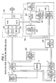
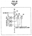
- FIG. 1 A block diagram of the complete trinary error detection and correction system is shown in Fig. 1.
- the data tryte (9 trits) is read from the trinary data source 2 into register 3 and also into check trit generator unit 100 by control 4.
- Check trit generator unit 100 develops four check trits for each tryte of nine data trits input as illustrated in Fig. 23. The four generated check trits are read into register 5 on lines CT1-1 to CT1-4.
- the nine trits are read into another check trit generator unit 200 for development of another four check trits as previously performed by check trit generator 100 at the time that the data tryte was originally read into register 3.
- the two pairs of four generated check trits from 100 via register 5 and from check trit generator unit 200 are then compared in check trit comparator unit 400.
- the comparator develops a syndrome trit for each of the four check trit comparisons and places the four syndrome trits developed on lines SY1-SY4 for input to the single error detector 600 and multiple error detector 700 in error detection unit 300.
- the data tryte read from register 3 is also directed to the data corrector 500 on lines D0-D8 as well as having been read into check trit generator unit 200.
- the data tryte will pass through the data corrector 500 either error free untouched, error free corrected, or with a multiple error-uncorrectable condition based on the syndrome trits developed in the check trit comparator unit 400.
- Each individual operation is shown in block diagram form in the figures and will be described in more detail as follows:
- MOSFET logic devices used in the trinary functional devices of the invention use the following basic parameters and functions as shown in Figure 18:
- MOSFET logic devices are used in describing the invention, any multi-level logic devices or circuitry could be used to perform the logic described in the specification.
- Fig. 3 Basic to the trinary error detection and correction of Fig. 1 is the check trit generator of Fig. 3 which develops a unique check trit for each pair of trinary trit inputs. Multiple check trit generators can be combined as shown in Fig. 4 to develop a check trit for multiple pairs of trinary trit inputs. This technique is used in the check trit generator units 100 and 200 where individual check trit generators are combined in several configurations.
- the check trit generator of Fig. 3 from a functional standpoint divides the trinary logic devices into three operating groups. The first group 174, including devices 141-148, based on the trinary input at B will set a trinary logic level on three points.
- the second group 175, including devices 149-152 based on the trinary input at A will open one of the points to permit the trinary level placed at that point by the B input to pass to an output point E.
- the third group 176, including devices 153-156 amplify the trinary level at the output point E. This amplified output is the particular trinary check trit for the trinary inputs at A and B.
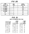
- the trinary logic devices shown in the circuit schematic of Fig. 3 follow the basic rules of operation shown in Fig. 20 for generating a check trit output for all possible combinations of trinary logic levels on the two inputs A and B.
- Fig. 22 indicates the conditions of all the devices of Fig. 3 and the logic levels at points C, D, E and the output check trit. Combining the basic rules of MOSFET operation shown in Fig, 20, and the MOSFET conditions in Figs. 21 and 22, the function of the check trit generator of Fig. 3 will be described.
- the logic input of zero (0) on line A causes 149 and 151 to be “off” since N-channel devices are “off” for a zero input and 150 and 152 will be “on” for a zero input.
- 149 "off” blocks the logic level at C from passing through to E.
- 151 "off” blocks logic level at point D from passing through 151 to 150 which is “on” to point E. Therefore, the level at point E will be controlled by 152 "on” passing the input on the B line to E. Since the level on B is zero, the level at E will be zero.
- the logic level of zero (0) on line B causes 143, 147, 145 and 146 to be "off” and 142, 141, 144 and 148 to be "on".
- 143 being off blocks the ground level (0) from passing through 142 (on) to the point C.
- 147 being off blocks the VCN level (logic 2) from passing through to point C.
- 141 being on will allow the VDD level (logic 1) to pass through to the point C.
- 149 being off from the zero level at input A blocks the passage of the VDD level (1) at point C from passing through to point E. Therefore, at point E will be zero (logic 0).
- the (0) level at E causes 156 and 153 to be “off” and 155, 154 to be “on” 156 being off blocks the passage of the VCN level (2) from passing through 155 to the output. 153 being “off” blocks the passage of the VDD level (1) from passing through to the output. However, 154 being “on” allows the ground level (0) to pass through to the output making the check trit output a (0) for an input of 0, 0.
- the trinary logic inputs at A and B control the CMOS devices to place either a ground level (0), a VCN level (2), or a VDD level (1) at point E.
- the logic level at point E controls the CMOS devices in the power amp to place the check trit output at a particular logic level.
- a (1) level at E will cause 155 and 154 to be “off” and 156 and 153 to be “on”. 155 being “off” blocks the VCN (2) output and 154 being “off” blocks the ground (0) output. 153 being “on” allows the VDD level (1) to pass to the check trit output. Therefore, for an input of 0, 1 the check trit is a (1).
- Vt1 devices of 155 and 156 will cause Vt1 devices of 155 and 156 to be "on” and the Vt2 devices of 153 and 154 to be “off".
- 154 being off blocks the ground level (0) and 153 being “off” blocks the VDD level (1).
- 155 and 156 being "on” allows the VCN level (2) to pass to the output. Therefore, for an input of 0, 2 the check trit is a (2).
- the devices 151, 149 will be “on” and devices 150 and 152 will be “off” based on the (1) input at A.
- devices 143, 147, 145 and 146 will be off and 142, 141, 144 and 148 will be “on”.
- 150 being off will block point D from affecting the output
- 152 being off will block point B from affecting point E.
- 149 being "on” will allow passage of point C to point E.
- 147 being off will block the VCN level (2) from passing to point C.
- 143 being “off” will block the ground level (0) from passing to point C. 141 being “on” will allow the VDD level (1) to pass to point C and through 149 to point E.
- the (1) at E will cause 156 and 153 to be “on” and 155 and 154 to be “off”. 155 being “off” blocks the passage of VCN while 154 being “off” blocks the passage of ground level (0) to the output. Therefore 153 being “on” controls the output by allowing passage of VDD (1) to the check trit output. Therefore, for an input of 1, 0 the check trit is (1).
- the devices 150 and 152 will be “off” and 151, 149 will be “on” based on the (1) input at A.
- Devices 141, 142, 144, and 148 will be “off” and 143, 145, 146 and 147 will be “on” based on the (1) input at B.
- 150 and 152 being “off” will block points D and B from passing to point E; therefore, the level at point C will pass through to point E.
- 142 being “off” will block the ground level through 143, and 141 being “off” will block the VDD level (1). Therefore, 147 being “on” allows the VCN level (2) to pass to point C and through 149 to point E.
- the (2) trinary logic level at E turns the Vt1 devices of 155 and 156 “on” and the Vt2 devices of 153 and 154 “off". 155 and 156 being “on” allows the VCN level (2) to pass to the check trit output. Therefore, for an input of 1, 1, the check trit is (2).
- the devices 150 and 152 will be “off” and 151, 149 will be “on” based on the (1) input at A.
- the Vt1 devices 142, 144, 143, 145 will be “on”
- Vt2 devices 141, 148, 147, 146 will be “off” based on the (2) input at B.
- the level at point C will pass through to point E.
- 142 and 143 being “on” will allow ground level (0) to pass to point C and through 149 "on” to point E.
- a (0) at point E will cause 155 and 154 to be “on” and 156 and 153 to be “off”.
- 156 blocks the VCN level
- 153 blocks the VDD level while 154 being “on” passes the ground level (0) to the check trit output. Therefore, for a 1, 2 input the check trit is (0).
- Vt1 devices 151 and 150 will be “on” and the Vt2 devices 149 and 152 will be “off” based on the (2) level input at A.
- Devices 141, 142, 144 and 148 will be “on”, and devices 143, 145, 146 and 147 will be “off”, based on the (0) level input at B.
- 151 and 150 being "on” will allow the level at point D to pass through to point E while 149 and 152 being “off” will block all other levels from passing to point E. 145 and 146 being “off” will block the VDD level and ground level, respectively, while 148 being “on” will reverse the VCN level (2) to point D and to point E through 151, 150.
- the (2) at E will turn “on” Vt1 devices 156 and 155 while turning “off” Vt2 devices 153 and 154. 153 and 154 block the VDD and ground levels, respectively, while 156 and 155 being “on” allow the VCN level (2) to pass to the output. Therefore, for a 2, 0 input the check trit is (2).
- Vt1 devices 151 and 150 will be “on”, and the Vt2 devices 149 and 152 will be “off”, based on the (2) level input at A.
- Devices 141, 142, 144 and 148 will be “off” and 143, 145, 146 and 147 will be “on”, based on the (1) input at B.
- the conditions of 150, 151, 149 and 152 will pass point D to point E.
- 144 and 148 being “off” will block VDD and VCN, respectively, from point D while 146 being “on” will pass level ground (0) to point D through 151 and 150 to point E.
- the (0) at point E will turn “on” 155 and 154 and turn “off” 156 and 153.
- 156 and 153 will block the VCN and VDD levels while 154 being “on” will pass ground level (0) to the output. Therefore, for a 2, 1 input, the check trit is (0).
- the Vt1 devices 143, 145, 151 142, 144 and 150 are "on” while the Vt2 device 147, 146, 149, 141, 148 and 152 are “off”.
- 152 blocks input B while 149 blocks point C from passing to E. 151 and 150 being “on” allow point D to pass to E. 148 and 146 being “off” block the VCN and ground levels from point D while 145 and 144 being “on” allow the VDD level (1) to pass to D and through 151, 150 to point E.
- the (1) at E turns 155, 154 “off” and 156, 153 "on”.
- the 155, 154 being “off” block VCN and ground levels while 153 being “on” allows the level (1) to pass to the output. Therefore, for a 2, 2 input, the check trit is a (1).
- the trinary check trit generator of Figure 3 therefore develops a trinary check trit 0, 1, 2 for all combinations of trinary logic levels on two inputs.
- the trinary check TRIT generator provides a check TRIT (equivalent to a parity bit in binary) based on input of trinary data (0, 1, 2) on two lines.
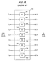
- the check trit generator tree combines a series of the 2-trit generators of Fig. 3 in a tree arrangement to generate a check trit for multiple pairs of trinary inputs.
- Four pairs of inputs To and T1, T2 and T3, T4 and T5, T6 and T7 are applied to trit generators 20, 21, 22 and 23, respectively.
- the four outputs from the trit generators are obtained as described for input A and B in Fig. 3.
- the four outputs 28, 29, 30 and 31 are combined in pairs and applied to trit generators 24 and 25.
- the two outputs from these generators on 32 and 33 are input to the final trit generator 26 and power amp 27 to obtain the check trit on output line 34.
- a single check trit is generated for an input of eight data trits.
- a combination of input lines and check trit generator configurations can be used to obtain a check trit.
- the trinary data source 2 in Fig. 1 is shown as a binary to trinary converter.
- the details of this converter are described in U.S. 4,631,428 to the same inventor and assignee. However, this is merely to illustrate a particular trinary data source.
- Trinary error detection and correction could be used with other sources of trinary data.
- the latch operates to latch in any of the trinary logic levels placed on the data-in line under control of the trinary clock. Provision is also made for scanning in test data.
- N channel and P channel MOSFETs are indicated by an N or P, respectively.
- Enhancement MOSFETs have a five-part gate.
- Vt1 and Vt2 are 1/4 of 3/4 of the absolute value of VDD.
- the +Vt is referenced to ground.
- the -Vt1 is referenced to +VDD.
- the threshold voltages are set as follows:
- the trinary clock has three functions:
- the clock's logic 1 is above 44's -Vt2, turning it off and inhibiting scan data input.
- the clock's logic 1 turns 43 on, but 42 is off; thus, the latchback from data output D0 to common connection A through 43-42 is inhibited.
- Data input is gated by a logic 1 level on the clock.
- the trinary level at node A controls 45, 46, and 48-47, providing an output at D0 equivalent to the signal at node A.
- a logic 1 at node A turns 45 on, sourcing D0 to +VDD, logic 1.
- a logic 0 at node A turns on 46, sinking D0 to ground, logic 0.
- a logic 2 at node A turns on 48 and 47, sourcing D0 to -VCN, logic 2.
- the latch condition is with the clock at logic 2.
- the clock switches from logic 1 to logic 2
- the data which was gated by clock logic 1 is latched by the clock logic 2 state.
- 41 switches off, and 43 and 42 switch on.
- 41 is turned off by the clock's +VCN level (logic 2) being below 41's +Vt2; therefore, input data is inhibited.
- 43 is turned on by the +VCN clock level being above its +Vt1
- 42 is turned on by the +VCN clock level being below its -Vt1.
- D0 is fed back through 43-42 to node A. This is the latch-up condition.
- input data is latched, because the clock 2 state was entered from clock 1 state.
- the latch condition is with the clock at logic 2.
- the clock switches from logic 0 to logic 2
- the scan data which was gated by clock logic 0 is latched by the clock logic 2 state.
- 44 switches off, and 43 and 42 switch on.
- 44 is turned off by the clock's +VCN level (logic 2) being above 44's -Vt2; therefore, scan data is inhibited.
- 43 is turned on by the +VCN clock level being above its +Vt1
- 42 is turned on by the +VCN clock level being below its -Vt1.
- D0 is fed back through 43-42 to node A. This is the latch-up condition.
- scan data is latched, because the clock 2 state was entered from clock 0 state.
- Input data/scan data is gated at the leading edge of clock logic level 1/0, respectively.
- the selected input is latched at the trailing edge of clock 1 or 0 transition to level 2. Input transitions between clocks have no effect on the latch.
- scan data is a don't-care; conversely, when scan data is being clocked by clock level 0, input data is a don't-care.
- the selected data/scan changes during a clock, the output changes accordingly, and the state of the selected input is latched when the clock switches to level 2.
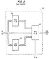
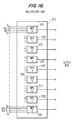
- the CTGU-2 register 3 receives a trinary tryte of data on lines D0-D8 from the trinary data source 2.
- the register comprises nine trinary latches 51-59 which store the individual trits under direction of the control unit 4. After a selected time the tryte stored in the register is read out to the data corrector 500, Fig. 2, and also to the check trit generator unit-2, 200 under direction of the control unit.
- a register is used as the storage device for purposes of describing the function of the invention, any trinary device which receives data which is to be checked for error upon a later read-out could be substituted.
- the CTGU-1 register 5 receives four check trits from CTGU-1 on lines CT1-1 to CT1-4 into trinary latches 61-64 The operation of the trinary latch is shown in Fig. 19. The four check trits are transferred from the register to the check trit comparator unit CTCU 400 under direction of the control unit.
- the control unit comprises a clocking system and combinatorial and sequential logic system for controlling the writing of trinary data into and the reading of trinary data out of the CTGU-1 and CTGU-2 registers.
- the trinary data is presented to CTGU-1 and CTGU-2 by the trinary data source 2.
- a signal from trinary data source 2 is sent to control 4 to indicate that trinary data is on the buss and ready for latching into CTGU-1 and CTGU-2 registers.
- control 4 provides the control signals and clocks to CTGU-1 and CTGU-2 registers to latch in the trinary data and trinary check trits.
- control 4 determines when new trinary data is needed from trinary data source 2 and sends a request signal to trinary data source 2.
- Control 4 waits a predetermined time for the trinary data to be presented by trinary data source 2 and generates the control signals and clocks to CTGU-1 and CTGU-2 registers to latch in the trinary data and trinary check trits.
- the trinary data is gated out of CTGU-1 and CTGU-2 registers by the control 4 at the appropriate time to be used by the device receiving by way of the data output bus, the corrected trinary data output of the trinary data error detection and correction system.
- CTGU-1 and CTGU-2 are functionally identical in generating four check trits for each data tryte of nine trits input.
- the basic functional unit used by the CTGUs is the check trit generator CTG shown in Fig. 3 and in a tree arrangement in Fig. 4.
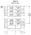
- check trit generator unit 100 provides four check trits according to the levels of the nine trinary data inputs D0-D8.
- CTG in circuits 101-134 is an abbreviation for check trit generator.
- the outputs of circuits 105-134 are labelled CT1-1 through CT1-4 for the check trits 1-4.
- the inputs to the check trit generator are connected following the table in Fig. 23, Four Trit Trinary Error Correction Codes (TECC).
- TECC Trit Trinary Error Correction Codes
- Circuits 101-105 generate check trit 1, CT1-1.
- check trit 1 has x's under data trits 0, 1, 3, 4, 6, and 8. (The x under data trit 10 is not used in this nine trit tryte -- data trit 8 is the last input used. The x's indicate which data trits are used to generate each check trit.
- D0 and D1 are connected to CTG 101.
- D3 and D4 are connected to CGT 102.
- D6 and D8 are connected to CTG 103.
- Each CTG circuit generates trinary parity (balance) on its output according to the trinary levels on its two inputs.
- D0-D8 are at trinary levels 012001122; D0, D1, D3, D4, D6, and D8 are trinary 010012, respectively.
- D0 and D1 inputs at trinary 0 and 1 into circuit 101 generates trinary parity 1.
- D3 and D4 inputs at trinary 0 and 0 into circuit 102 generates trinary parity 0.
- D6 and D8 inputs at trinary 1 and 2 into circuit 103 generates trinary parity 0.
- Circuits 101 and 102 provide trinary 1 and 0 into circuit 104 which generates a trinary 1 parity.
- Circuits 104 and 103 provide trinary 1 and 0 into circuit 105 which generates a trinary 1 parity.
- the output of circuit 105 is the resultant CT1-1 (check trit unit 1, check trit 1).
- Circuits 111-114 generate check trit 2, CT1-2.
- check trit 2 has x's under the data trits 0, 2, 3, 5, and 6. (The x's under data trits 9 and 10 are not used in this nine trit tryte -- data trit 8 is the last input used).
- D0 and D2 are connected to CTG 111.
- D3 and D5 are connected to CTG 112.
- D6 is connected to CTG 114.
- Each CTG circuit generates trinary parity on its output according to the trinary levels on its two inputs.
- Circuits 111 generates trinary parity on the D0 and D2 inputs.
- Circuit 112 generates trinary parity on the D3 and D5 inputs.
- Circuit 113 generates trinary parity on the outputs of circuits 111 and 112.
- Circuit 114 generates trinary parity on the output of circuit 113 and D6.
- D0 and D2 inputs at trinary 0 and 2 into circuit 111 generates trinary parity 2.
- D3 and D5 inputs at trinary 0 and 1 into circuit 112 generates trinary parity 1.
- Circuits 111 and 112 provide trinary 2 and 1 into circuit 113 which generates a trinary 0 parity.
- Circuit 113 and D6 provide trinary 0 and 1 into circuit 114 which generates a trinary 1 parity.
- the output of circuit 113 is the resultant CT1-2 (check trit unit 1, check trit 2)
- Circuits 121-124 generate check trit 3, CT1-3.
- check trit 2 has x's under data trits 1, 2, 3, 7, and 8. (The x's under data trits 9 and 10 are not used in this nine trit tryte -- data trit 8 is the last input used).
- D1 and D2 are connected to CTG 121.
- D3 and D7 are connected to CTG 122.
- D8 is connected to CTG 124.
- Each CTG circuit generates trinary parity on its output according to the trinary levels on its two inputs.
- Circuit 121 generates trinary parity on the D1 and D2 inputs.
- Circuit 122 generates trinary parity on the D3 and D7 inputs.
- Circuit 123 generates trinary parity on the outputs of circuits 121 and 122.
- Circuit 124 generates trinary parity on the output of circuit 123 and D8.
- D0-D8 are at trinary levels 012001122; D1, D2, D3, D7, and D8 are trinary 12022, respectively.
- D1 and D2 inputs at trinary 1 and 2 into circuit 121 generates trinary parity 0.
- D3 and D7 inputs at trinary 0 and 2 into circuit 122 generates trinary parity 2.
- Circuits 121 and 122 provide trinary 0 and 2 into circuit 123 which generates a trinary 2 parity.
- Circuit 123 and D8 provide trinary 2 and 2 into circuit 124 which generates a trinary 1 parity.
- the output of circuit 123 is the resultant CT1-3 (check trit unit 1, check trit 3).
- Circuits 131-134 generate check trit 4, CT1-4.
- check trit 3 has x's under data trits 4, 5, 6, 7, and 8. (The x's under data trits 9 and 10 are not used in this nine trit tryte -- data trit 8 is the last input used).
- D4 and D5 are connected to CTG 131.
- D6 and D7 are connected to CTG 132.
- D8 is connected to CTG 134.
- Each CTG circuit generates trinary parity on its output according to the trinary levels on its two inputs.
- Circuit 131 generates trinary parity on the D4 and D5 inputs.
- Circuit 132 generates trinary parity on the D6 and D7 inputs.
- Circuit 133 generates trinary parity on the outputs of circuits 131 and 132.
- Circuit 134 generates trinary parity on the output of circuit 133 and D8.
- D0-D8 are at trinary levels 012001122; D4, D5, D6, D7, and D8 are trinary 01122, respectively.
- D4 and D5 inputs at trinary 0 and 1 into circuit 131 generates trinary parity 1.
- D6 and D7 inputs at trinary 1 and 2 into circuit 132 generates trinary parity 0.
- Circuits 131 and 132 provide trinary 1 and 0 into circuit 133 which generates a trinary 1 parity.
- Circuit 133 and D8 provide trinary 1 and 2 into circuit 134 which generates a trinary 0 parity.
- the output of circuit 133 is the resultant CT1-4 (check trit unit 1, check trit 4).
- check trit generator unit 200 provides four check trits according to the levels of the nine trinary data inputs D0-D8.
- CTG in circuits 201-234 is an abbreviation for check trit generator.
- the outputs of circuits 205-234 are labelled CT2-1 through CT2-4 for the check trits 1-4.
- the inputs to the check trit generator are connected per the table in Fig. 23, Four Trit Trinary Error Correction Codes (TECC).
- TECC Trit Trinary Error Correction Codes
- Circuits 201-205 generate check trit 1, CT2-1.
- check trit 1 has x's under data trits 0, 1, 3, 4, 6, and 8. (The x under data trit 10 is not used in this nine trit tryte -- data trit 8 is the last input used0. The x's indicate which data trits are used to generate each check trit.
- D0 and D1 are connected to CTG 201.
- D3 and D4 are connected to CGT 202.
- D6 and D8 are connected to CTG 203.
- Each CTG circuit generates trinary parity (balance) on its output according to the trinary levels on its two inputs.
- D0-D8 are at trinary levels 012001122; D0, D1, D3, D4, D6, and D8 are trinary 010012, respectively.
- D0 and D1 inputs at trinary 0 and 1 into circuit 201 generates trinary parity 1.
- D3 and D4 inputs at trinary 0 and 0 into circuit 202 generates trinary parity 0.
- D6 and D5 inputs at trinary 1 and 2 into circuit 203 generates trinary parity 0.
- Circuits 201 and 202 provide trinary 1 and 0 into circuit 204 which generates a trinary 1 parity.
- Circuits 204 and 203 provide trinary 1 and 0 into circuit 205 which generates a trinary 1 parity.
- the output of circuit 205 is the resultant CT2-1 (check trit unit 2, check trit 1).
- Circuits 211-214 generate check trit 2, CT2-2.
- check trit 2 has x's under the data trits 0, 2, 3, 5, and 6. (The x's under data trits 9 and 10 are not used in this nine trit tryte -- data trit 8 is the last input used).
- D0 and D2 are connected to CTG 211.
- D3 and D5 are connected to CTG 212.
- D6 is connected to CTG 214.
- Each CTG circuit generates trinary parity on its output according to the trinary levels on its two inputs.
- Circuits 211 generates trinary parity on the D0 and D2 inputs.
- Circuit 212 generates trinary parity on the D3 and D5 inputs.
- Circuit 113 generates trinary parity on the outputs of circuits 211 and 212.
- Circuit 214 generates trinary parity on the output of circuit 213 and D6.
- D0 and D2 inputs at trinary 0 and 2 into circuit 211 generates trinary parity 2.
- D3 and D5 inputs at trinary 0 and 1 into circuit 112 generates trinary parity 1.
- Circuits 211 and 212 provide trinary 2 and 1 into circuit 213 which generates a trinary 0 parity.
- Circuit 213 and D6 provide trinary 0 and 1 into circuit 214 which generates a trinary 1 parity.
- the output of circuit 213 is the resultant CT2-2 (check trit unit 2, check trit 2).
- Circuits 221-224 generate check trit 3, CT2-3.
- check trit 2 has x's under data trits 1, 2, 3, 7, and 8. (The x's under data trits 9 and 10 are not used in this nine trit tryte -- data trit 8 is the last input used).
- D1 and D2 are connected to CTG 121.
- D3 and D7 are connected to CTG 222.
- D8 is connected to CTG 224.
- Each CTG circuit generates trinary parity on its output according to the trinary levels on its two inputs.
- Circuit 221 generates trinary parity on the D1 and D2 inputs.
- Circuit 222 generates trinary parity on the D3 and D7 inputs.
- Circuit 223 generates trinary parity on the outputs of circuits 221 and 222.
- Circuit 224 generates trinary parity on the output of circuit 223 and D8.
- D0-D8 are at trinary levels 012001122; D1, D2, D3, D7, and D8 are trinary 12022, respectively.
- D1 and D2 inputs at trinary 1 and 2 into circuit 221 generates trinary parity 0.
- D3 and D7 inputs at trinary 0 and 2 into circuit 222 generates trinary parity 2.
- Circuits 221 and 222 provide trinary 0 and 2 into circuit 223 which generates a trinary 2 parity.
- Circuit 223 and D8 provide trinary 2 and 2 into circuit 224 which generates a trinary 1 parity.
- the output of circuit 223 is the resultant CT2-3 (check trit unit 2, check trit 3).
- Circuits 231-234 generate check trit 4, CT1-4.
- check trit 3 has x's under data trits 4, 5, 6, 7, and 8. (The x's under data trits 9 and 10 are not used in this nine trit tryte -- data trit 8 is the last input used).
- D4 and D5 are connected to CTG 231.
- D6 and D7 are connected to CTG 232.
- D8 is connected to CTG 234.
- Each CTG circuit generates trinary parity on its output according to the trinary levels on its two inputs.
- D0-D8 are at trinary levels 012001122; D4, D5, D6, D7, and D8 are trinary 01122, respectively.
- D4 and D5 inputs at trinary 0 and 1 into circuit 231 generates trinary parity 1.
- D6 and D7 inputs at trinary 1 and 2 into circuit 232 generates trinary parity 0.
- Circuits 231 and 232 provide trinary 1 and 0 into circuit 233 which generates a trinary 1 parity.
- Circuit 233 and D8 provide trinary 1 and 2 into circuit 234 which generates a trinary 0 parity.
- the output of circuit 233 is the resultant CT2-4 (check trit unit 2, check trit 4).
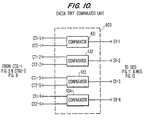
- Fig. 10 illustrates the circuit schematic for the check trit comparator unit 400 (Fig. 1) used for comparing check trits.
- Fig. 10A illustrates the logic operation of the trinary logic comparator which is the basic unit 431-434 of the check trit comparator unit 400 (Fig. 10).
- two trinary level signals A and B
- a and B are input at four points, and based on the compared values of A and B, a trinary output is obtained.
- the outputs are:
- the TCLC circuit schematic is in Fig. 10A.
- N channel and P channel MOSFETs are indicated by an N or P, respectively.
- Enhancement MOSFETs have a three-part gate.
- Vt1 and Vt2 are one fourth or three fourths of the absolute value of VDD.
- the +Vt is referenced to ground.
- the -Vt is referenced to +VDD.
- the threshold voltages are set as follows:
- the output is (0) Gnd when A is less than B.
- the output is sunk to Gnd by 404-403.
- 403 is on when A is 0, and 404 is on when B is not 0.
- A is less than B in both A0B1 and A0B2.
- the output is also sunk to Gnd by 410-409-408.
- 408 is on when B is below 3/4 VDD, and 409 is on when B is above 1/4 VDD; therefore, they are both on when B is at the centre voltage level. So, the output equals 0 when the inputs are A1B2; again, by inspection, note that A1 is less than B2.
- the output is (1) + VDD when A is greater than B.
- the output is sourced to +VDD by 402-401.
- 402 is on when A is not 0, and 401 is on when B is 0.
- A is greater than B in both A1B0 and A2B0.
- the output is also sourced to +VDD by 407-406-405.
- 405 is on when A is below 3/4 VDD, and 406 is on when A is above 1/4 VDD; therefore, they are both on when A is at the centre voltage level. So, the output equals 1 when the inputs are A2B1; again, by inspection, note that A2 is greater than B1.
- the inputs are equal (A0B0, AlBl, or A2B2), the output is 2.
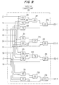
- the check trit comparator unit 400 is comprised of four individual trinary logic comparators 431-434. Each comparator receives two check trits with the first one being on the CT1 line from CTG-1 via register 5 and the second one being on the CT2 line from CTG-2. Each of the comparators 431-434 operates individually as described for Fig. 10A to produce four syndrome trits on SY-1 to SY-4, respectively. These are transferred to both the Single Error Detector 600 (SED) and also the Multiple Error Detector 700 (MED).
- SED Single Error Detector 600
- MED Multiple Error Detector 700
- the single error detector unit 600 monitors the four Syndrome trits (SY1-SY4) to detect a discrete single data trit error.
- the nine output select trits (S0-S8) are used by the data corrector 500 to select either an incremented, decremented, or as-is trit from register 3 to provide error-free data trits on the output of the trinary error correction code system. Only one of the select lines become active as a 0 or 1 when a single trit error is encountered; the other eight select lines will be trinary 2, indicating that the associated data trit has no error.
- single error detector circuit trit 0 is an expanded schematic of circuit 610 in single error detector 600.
- Circuits 611, 612, 613 in the single error detector circuit trit 0 are expanded schematics of circuits 611, 612, and 613 in the single error detector 600.
- the nine select outputs each indicate one of the following conditions on its associated trinary data trit: trinary 1 indicates that the input data trit has been incremented, trinary 0 indicates that the input data trit has been decremented, and trinary 2 indicates that no error exists on that data trit.
- an incrementation error on data trit 0 is indicated by SY1-SY4 being only 1122, at which time the four sensors in circuit 611 are active sourcing the output to VDD for a trinary 1.
- a decrementation error on data trit 0 is indicated by SY1-SY4 being only 0022, at which time the four sensors in circuit 513 are active sinking the output to ground for a trinary 0.
- a no-error condition is indicated by SY1-SY4 being 2222, at which time the four sensors in circuit 612 are active sourcing the output to VCN for a trinary 2.
- the syndrome trits are not all 2222; thus, the other eight trits' single error detectors no not receive a no-error indication on the syndrome trits. If the syndrome trits are 1211 indicating that data trit 8 was incremented, detectors 612, 622, 632, 642, 652, 662, 672 and 682 do not receive 2222, preventing the S0-S8 outputs from being sourced to VCN for trinary 2's. Addition of the pull-up resistors on the outputs performs the function of pulling the outputs to VCN any time that none of the active circuits, i.e., 611, 612, and 613 for trit 0, are selected.
- the syndrome trits will be 2222 indicating no-error with active pull-up to VCN for all nine trits. Only when an error is encountered will the pull-up resistors become effective for the select lines without the error.
- single error OR circuit 650 performs an OR function on the nine selection lines (S0-S8) to provide a single line which indicates single error.
- the circuits 614-694 monitor for a level NOT2 (a "1" or "0") on the select lines; if any one of the nine lines is at level 1 or 0, the output goes to level 1, indicating a single trit error. When all of the select lines are level 2, the output goes to level 0, indicating NOT a single error.
- the NED (800) receives the nine select lines (S0-S8) from the SED 600.
- the no-error detector performs an AND function on the nine select lines (S0-S8) to provide a single line which indicates no error.
- the circuits 801-912 monitor for a level 2 (not 1 and not 0) on the select lines. When all nine select lines are level 2 (no error), the output goes to level 1 to indicate no-error condition on the entire data tryte. If any one of the nine select lines is at level 1 or 0 (an incremented error or a decremented error, respectively) the output goes to level 0, indicating that the data tryte has an error.
- Select lines S0, S1, and S2 are ANDed together in circuits 801, 802, and 803; select lines S3, S4, and S5 are ANDed together in circuits 804, 805, and 806; and select lines S6, S7, and S8 are ANDed together in circuits 807, 808, and 809.
- the three ANDed signals are then ANDed together in circuit 810, 811, and 812 to provide an output line 813 indicating no-error.
- circuits 810, 811, and 812 When all three inputs to circuits 810, 811, and 812 are at level 1, all three circuits are gated on, thus, the output 813 is sourced to VDD (level 1) indicating no-error condition.
- circuits 810, 811, and 812 When any one of the three inputs to circuits 810, 811, and 812 are at level 0, the circuit which that signal drives is degated.
- the output 813 is at level 1 indicating no-error.
- the overall AND function is broken, and the output 813 goes to ground (level 0) indicating that one of the data trits has an error.
- the multiple error detection unit 700 monitors the four syndrome trits (SY1-SY4) to detect a multiple data trit error, more than one trit in error.
- the output of this detector consists of one output which indicates a multiple trit error has been detected when it is at level 1.
- the select lines S0-S8 will all be pulled up to level 2. By not being level 0 or 1, the select lines indicate that a single trit error does not exist -- it is not saying that a multiple trit error does not exist. More checking is needed to sense a multiple trit error.
- the no-error indicator input to circuit 704 of the multiple error detector 700 comes from the no-error detector 800.
- Circuit 704 is gated on when the no-error indicator is level 1 as noted inside circuit 704.
- Circuit 704 is in series (AND) with the paralleled circuits 705, 706, and 707 (OR).
- the no-error indicator from 800 is level 1 when all select lines (S0-S8) are level 2. This will occur when a multiple trit error exists.
- An incrementation error on data trit 0 is indicated by SY1-SY4 being only 1122, at which time the four sensors in circuit 611 are active sourcing the output to VDD for a trinary 1.
- a decrementation error on data trit 0 is indicated by SY1-SY4 being only 0022, at which time the four sensors in circuit 613 are active sinking the output to ground for a trinary 0.
- a no-error condition is indicated by SY1-SY4 being 2222, at which time the four sensors in circuit 612 are active sourcing the output to VCN for a trinary 2.
- the multiple error detector monitors the positions in Fig. 23 which do NOT have an x.
- the empty positions must be trinary 2 on the associated check trit.
- the multiple error detection consists of circuits 701-707.
- the comparators (701, 702, and 703) are trinary comparators.
- the comparator's output is at one of three trinary levels. Either a trinary 1 or 0 indicates a miscompare on the two inputs.
- a level 1 on the output of 701 indicates that SY1 is greater than SY2.
- a level 0 on the output of 701 indicates that SY1 is less than SY2.
- a trinary 2 indicates a compare of the two inputs.
- a level 2 on the output of 701 indicates that SY1 is equal to SY2.
- all four syndrome trits (SY1-SY4) are at level 2.
- the no-error indicator from the no-error detector 800 will be at level 1 (no error) because of the following: all four syndrome trits (SY1-SY4) being at levels 2222 into the single error detector 600 gates the circuits 612, 622, 632, 642, 652, 662, 672, 682, and 692 ON, generating level 2's on select lines (S0-S8); and the select lines' all being level 2 generates level 1 on the no-error indicator.
- the no-error indicator gates circuit 704 ON to sample for multiple errors in the multiple error detector 700. With all four syndrome trits (SY1-SY4) are level 2, the outputs from circuits 701, 702, and 703 at level 2 indicating compares on the input syndrome trits.
- the multi-error output is not sourced to VDD and the output is level 0 indicating that a multi-error does not exist.
- the no-error indicator from the no-error detector 800 will be at level 1 (no error) because of the following: the four syndrome trits' code does not match any of the single error detection codes, and does not match the 2222 code -- the select lines are sourced to VCN (level 2) via the resistors; and the select lines' all being level 2 generates level 1 on the no-error indicator.
- the no-error indicator gates circuit 704 ON to sample for multiple errors in the multiple-error detector 700.
- the outputs from comparators 701, 702, and 703 are not all level 2 indicating a miscompare in at least one of the three comparators.
- the SY1 and SY2 not being a match into comparator 701 generates the miscompare output level 0.
- the SY2 and SY3 not being a match into comparator 702 generates the miscompare output level 0.
- the SY3 and SY4 not being a match into comparator 703 generates the miscompare output level 0.
- the miscompare level 0 on the output of either of the three comparators 701, 702, or 703 gates ON the NOT2 sensor 705, 706, or 707, respectively.
- Comparator 701's output being at level NOT2 (1 or 0) gates NOT2 sensor 705. Comparator 702's output being at level NOT2 (1 or 0) gates NOT2 sensor 706. Comparator 703's output being at level NOT2 (1 or 0) gates NOT2 sensor 707. With at least one of the NOT2 sensors being gated, the multi-error output is sourced to VDD through circuit 704, and the output is level 1 indicating that a multi-error does exist.
- error indicator 750 generates a single trinary output which indicates the error status of the data tryte.
- Level 1 indicates single error.
- Level 2 indicates no error.
- Level 0 indicates multiple error.
- level 1 on the single error indicator from 650 gates level 1 sensor 751 ON, sourcing the output to VDD for level 1 (single error); also, NOT1 sensor 753 is degated.
- level 1 on the multiple error indicator from 700 gates level 1 sensor 752 ON, sinking the output to ground for level 0 (multiple error); also, NOT1 sensor 754 is degated.
- level 0 on the single error indicator from 650 degates level 1 sensor 751 OFF, inhibiting sourcing the output to VDD; also, NOT1 sensor 753 is gated ON.
- level 0 on the multiple error indicator from 700 degates level 1 sensor 752 OFF, inhibiting sinking the output to VDD; also, NOT1 sensor 754 is gated ON. With both NOT1 sensors 753 and 754 gated ON, the output is sourced to VCN for level 2 (no error).
- the data corrector includes the multiplexer unit 570, decrementor unit 540 and incrementor unit 520. Under control of the S0-S8 select trit signals from the single error detector, the multiplexer unit selects either the incremented data tryte, the decremented data tryte, or the unaltered data tryte for passage to the output bus.
- the trinary decrementor unit (TDU) 540 shown in Fig. 15 is made up of individual decrementors as shown in detail in Fig. 15A. Referring to Fig. 15A, the decrementor decrements an input by subtracting one from a trinary input underflowing to two when decrementing from zero.
- 551 and 552 are “1” while 553 and 554 are “off”. 553 being off blocks gnd (0) from the output while 554 being off blocks VCN from the output. 551 and 552 being "on” passes VDD (1) thus setting the output line at (1).
- the decrementor unit DEC which is made up of individual decrementor units 541-549, decrements each of the nine trits on data lines D0-D8 and passes on the decremented output to the multiplexer 570.
- the trinary incrementor unit 520 shown in Fig. 2 comprises individual incrementors as shown in detail in Fig. 14A.
- an incrementor increments an input by adding one to a trinary level input overflowing to zero when incrementing a 2.
- 531 and 532 are "on” while 533 and 534 are “off”.
- 553 being “off” blocks ground from the output line 535 while 534 being “off” blocks VCN (2) from the output line 535.
- 531 being “on” allows VDD (trinary logic 1 level) to set the output line 535 at "1".
- the trinary logic incrementor unit made up of individual incrementors 521-529 increments each of the nine trits on data lines D0-D8 and passes on the incremented output to multiplexer 570.
- the MPXU (570) of Fig. 16 comprises nine individual multiplexors 571-579 which select one of three input lines for placing that particular trinary level on the output bus. Based on the trinary value on the select line, the multiplexor 570 places the input level from either the read data trit, or the decrementor 540, or the incrementor 520 on the output bus.
- the select line at logic level 2 indicates a "no error" or equal condition, and therefore the read data line D2 is selected with no correction needed.
- the select line at logic level 1 indicates that the data has increased by logic level 1 and therefore the decrementor input line 540 on D1 which has been decreased by logic level 1 is selected for output thus performing a data correction.
- the select line at logic level 0 indicates that the data has decreased by logic level 1, and therefore, the incrementor input from 520 on D0 which has been increased by logic level 1 is selected for output thus performing a data correction.
- the trinary select lines function as follows:
- the individual multiplexors operate as follows:
- the three conditions which can exist for handling data by the trinary error detection and correction system of the invention are no-error, single error, and multiple error. An example of each of these three conditions will be executed through the system.
- Input data trits D0-D9 from trinary data source (2) 012001122 into check trit generator unit 100 into the CTG-2 register (3).
- the check trit comparator 400 compares the outputs of the check trit generator number 1 with the outputs of check trit generator number 2 to generate the syndrome trits (SY1-SY4).
- the single error detector 600 monitors the syndrome trits SY1-SY4 which are 2222.
- AND circuits 612, 622, 632, 642, 652, 662, 672, 682, and 692 are all active sourcing the select trits S0-S8 to VCN for level 2 indicating that every data trit is correct and no error correction is needed.
- the select trits are 222222222.
- the S0-S8 select trit lines being all 2's to the multiplexor unit 570 activate the multiplexors 571-579 to gate the D0-D8 data lines through to the data output bus in the uncorrected or original condition.
- the single error detector circuit trit 0 is an expanded circuit of the trit 0 on the single error detector 600.
- SY1-SY4 are 2222 on the inputs.
- AND circuit 611 has the top two level 1 sensors turned OFF, and the bottom two are ON.
- the series string is broken by either of the top two being OFF, and circuit 611 does not source the output to VDD level 1.
- AND circuit 613 has the top two level 0 sensors turned OFF, and the bottom two are ON.
- the series string is broken by either of the top two being OFF, and circuit 613 does not sink the output to Gnd level 0.
- AND circuit 612 has all four level 1 sensors turned ON.
- the series string is connected from VCN to the output, and AND circuit 612 does source the output to VCN level 2, indicating that data trit 0 has no error.
- the single error OR circuit 650 OR's the select trits S0-S8 to check for the presence of any data trits needing to be corrected. With 222222222 input, all of the NOT2 sensors are OFF, and the output is not sourced to VDD -- the output is level 0, indicating that no single trit error exists.
- the no-error detector 800 performs an AND function on the nine select trits S0-S8. All nine of the level 2 sensors, circuits 801-809 are ON with 222222222 input. The trinary signals on the outputs of 803, 806, and 809 are 111, which are ANDed in 810, 811, and 812 sourcing the output 813 to VDD level 1. Trinary logic level 1 on the no error indicator signals that no single trit error exists.
- the multiple error detector 700 checks the syndrome trits SY1-SY4 for inconsistency among the four syndrome trits.
- the no error indicator could be all 2's because of a multiple trit error, being pulled to VCN by the resistors in the single error detector when no syndrome code matches any of the codes for single errors.
- the no error indicator is 1 in this case of multiple error; the no error indicator indicates that there are no single trit errors.
- the three "not 2" sensors, 705, 706, and 707, need only one of them to be active to complete the path for sourcing the output to VDD for level 1, indicating that a multiple error exists. All three of the "not 2" sensors must be OFF to not indicate multiple trit error, as is the case in this example of no errors.
- the error indicator 750 generates the error indicator.
- the single error indicator from 650 is level 0, turning OFF the "1" sensor 751 and turning ON the “not 1” sensor 753.
- the multiple error indicator from 700 is level 0, turning OFF the "1" sensor 752 and turning ON the "not 1” sensor 754. Circuits 753 and 754 being ON completes the sourcing path to VCN, and the output is trinary logic level 2, which indicates that no error exists.
- the trit on the D0 line of the tryte has been assumed to have incremented from 0 to 1 in the transfer of the tryte through the CTG-2 register.
- the tryte was read into the register as [0]12001122 and read out at [1]12001122. Therefore the check trits generated by CTGU-1 will differ from CTGU-2.
- the check trit comparator unit 400 compares the outputs of the check trit generator number 1 with the outputs of check trit generator number 2 to generate the syndrome trits (SY1-SY4).
- the single error detector 600 monitors the syndrome trits SY1-SY4 which are 1122.
- AND circuits 611 is the only active sensor in the single error detector, sourcing the select trit 0 (S0) to VDD for level 1 indicating that data trit 0 has been incremented and needs to be decremented to correct the error.
- S1-S8 are all pulled up to VCN by the resistors for level 2 indicating that no error exists on data trits D1-D8.
- the select trits are 122222222.
- the S0 select trit line being "1" to the multiplexor unit 571 gates the decrement input DEC-0 through to the data output bus.
- the DEC-0 input is the input on line D0 from CTG-2 register (3) decremented by 1. Since the output on D0 from the CTG-2 register is 1, the decremented trit to multiplexor 571 is "0". Therefore the "0" on the output bus on D0 represents a correction to the first trit position of the tryte.
- the remaining select trit lines S1-S8 are 2's and will gate the data on lines D1-D8 through multiplexors 572-579 uncorrected.
- the single error detector circuit trit 0 is an expanded circuit of the trit 0 on the single error detector 600.
- SY1-SY4 are 1122 on the inputs.
- AND circuit 611 has all four sensors turned ON.
- the series string is connected from VDD to the output, and circuit 611 sources the output to VDD level 1, indicating that data trit 0 has been incremented.
- AND circuit 612 has the top two level 2 sensors turned OFF, and the bottom two are ON.
- the series string is broken by either of the top two being OFF, and circuit 612 does not sink the output to VCN level 2.
- AND circuit 613 has the top two level 0 sensors turned OFF, and the bottom two are ON.
- the series string is broken by either of the top two being OFF, and circuit 613 does not sink the output to Gnd level 0.
- the single error OR circuit 650 OR's the select trits S0-S8 to check for the presence of any data trits needing to be corrected. With 122222222 input, "not 2" sensor 614 is ON, and “not 2" sensors 624-694 are OFF. Sensor 614 being ON sources the output to VDD. The output is level 1, indicating that a single trit error exists.
- the no-error detector 800 performs an AND function on the nine select trits S0-S8.
- Level 2 sensor 801 is OFF, and 802-809 are all ON with 122222222 input.
- the trinary signals on the outputs of 803, 806, and 809 are 011, which are ANDed in 810, 811, and 812 -- 812 is OFF, inhibiting sourcing the output 813 to VDD level 1.
- the output is level 0, indicating a single trit error condition.
- the multiple error detector 700 checks the syndrome trits SY1-SY4 for inconsistency among the four syndrome trits.
- the no error indicator could be all 2's because of a multiple trit error, being pulled to VCN by the resistors in the single error detector when no syndrome code matches any of the codes for single errors.
- the no error indicator is 0 in this case of a single error, and multiple error path to VDD is broken.
- the output goes to level 0 no matter what the three comparators indicate.
- the level 0 on multi-error indicates that no multiple trit error exists.
- the error indicator 750 generates the error indicator.
- the single error indicator from 650 is level 1, turning ON the level 1 sensor 751 and turning OFF the NOT1 sensor 753.
- the multiple error indicator from 700 is level 0, turning OFF the level 1 sensor 752 and turning ON the NOT1 sensor 754. Circuit 751 being ON completes the sourcing path to VDD, and the output is trinary logic level 1, which indicates that a single trit error exists.
- the first two trits on the D0 and D1 line of the tryte from the data source have been assumed to have incremented from 0 to 1 and 1 to 2, respectively, in the transfer of the tryte through the CTG-2 register (3).
- the tryte was read into the register as [01]2001122 and read out of the register as [12]2001122. Therefore, the check trits generated by the CTGU-1 will differ from the CTGU-2.
- the check trit comparator 400 compares the outputs of the check trit generator number 1 with the outputs of check trit generator number 2 to generate the syndrome trits (SY1-SY4).
- the single error detector 600 monitors the syndrome trits SY1-SY4 which are 0112. No single error sensors are active in the single error detector; neither are any 2222 sensors. All of the select trits S0-S8 are pulled up to VCN by the resistors for level 2 indicating that no single trit error exists on data trits D0-D8. The select trits are 2222222222.
- the select bit lines S0-S8 being all 2's to multiplexers 571-579 gate the data lines D0-D8 through to the output bus uncorrected functioning identical to the no-error condition since multiple errors cannot be corrected.
- the multiple error indicator from the EI unit 750 can be used to activate the stop or recovery procedures.
- the single error detector circuit trit 0 is an expanded circuit of the trit 0 on the single error detector 600.
- SY1-SY4 are 0112 on the inputs.
- AND circuit 611, 612, nor 613 completes a path to any of the three trinary levels.
- circuit 611 only the second and fourth sensors are ON -- a 1 input to a 1 sensor, and 2 input into a 2 sensor.
- circuit 612 only the fourth sensor is ON -- a 2 input to a 2 sensor.
- circuit 613 only the first and fourth sensors are ON -- a 0 input into a 0 sensor and a 2 input to a 2 sensor.
- the output is pulled up to VCN by the pull resistor.
- the single error OR circuit 650 OR's the select trits S0-S8 to check for the presence of any data trits needing to be corrected. With 222222222 input, all of the NOT2 sensors are OFF, and the output is not sourced to VDD -- the output is level 0, indicating that no single trit error exists.
- the no error detector 800 performs an AND function on the nine select trits S0-S8. All nine of the level 2 sensors, circuit 801-809 are ON with 222222222 input. The trinary signals on the outputs of 803, 806, and 809 are 111, which are ANDed in 810, 811, and 812 sourcing the output 813 to VDD level 1. Trinary logic level 1 on the no error indicator signals that no single trit error exists.
- the multiple error detector 700 checks the syndrome trits SY1-SY4 for inconsistency among the four syndrome trits.
- the no error indicator could be all 2's because of a multiple trit error, as in this example, being pulled to VCN by the resistors in the single error detector when no syndrome code matches any of the codes for single errors.
- the no error indicator is 1 in this case of multiple errors; the no error indicator indicates that there are no single trit errors.
- the three "not 2" sensors, 705, 706, and 707 need only one of them to be active to complete the path for sourcing the output to VDD for level 1, indicating that a multiple error exists.
- the output is sourced to VDD via 704.
- the output is level 1, indicating that a multiple trit error exists.
- the error indicator 750 generates the error indicator.
- the single error indicator from 650 is level 0, turning OFF the "1" sensor 751 and turning ON the “not 1” sensor 753.
- the multiple error indicator from 700 is level 1, turning ON the "1" sensor 752 and turning OFF the "not 1” sensor 754. Circuit 752 being ON completes the sinking path to ground, and the output is trinary logic level 0, which indicates that a multiple error condition exists.
- the trinary "trit" of data would be replaced by a "piece" of data of level 0, or 1, or 2, or------n, and a selected number of pieces of data would comprise a "segment" of data equivalent to the trinary "tryte”.
- component sub-units could be used to replace, for example, the check trit generators, trinary latches, trinary comparators and trinary multiplexors specifically disclosed herein.
Landscapes
- Engineering & Computer Science (AREA)
- Theoretical Computer Science (AREA)
- Physics & Mathematics (AREA)
- Probability & Statistics with Applications (AREA)
- Detection And Correction Of Errors (AREA)
- Logic Circuits (AREA)
- Techniques For Improving Reliability Of Storages (AREA)
- Error Detection And Correction (AREA)
Claims (23)
- Ein Verfahren zum Generieren eines trinären Prüftrit der trinären Logikebene 0, 1 oder 2 für erste und zweite Eingabetrits, wobei das Verfahren folgendes einschließt:Anwenden des ersten Eingabetrit auf eine erste Eingabe (B) eines Prüftrit-Generators;Einstellen der trinären Logikebene jeweils an einem ersten Schaltpunkt (C) und einem zweiten Schaltpunkt (D) im Trit-Generator in Abhängigkeit vom ersten Eingabetrit über eine erste Gruppe trinärer Logikeinheiten (174) des mit der ersten Eingabe (B) verbundenen Trit-Generators;Anwenden des zweiten Eingabetrits auf eine zweite Eingabe (A) des Trit-Generators;Auswählen der trinären Logikebene entweder am ersten Schaltpunkt (C) oder am zweiten Schaltpunkt (D) und der ersten Eingabe (B) in Reaktion auf das zweite Eingabetrit über eine zweite Gruppe trinärer Logikeinheiten (175) des mit der zweiten Eingabe verbundenen Prüftrit-Generators;Einstellen der trinären Logikebene einer Ausgabezeile (E) in Abhängigkeit von der gewählten trinären Logikebene;wodurch die auf die Ausgabezeile (E) angewandte trinäre Logikebene von der Kombination der auf das erste und zweite Eingabetrit angewandten Logikebenen abhängt.
- Ein trinärer Prüftrit-Generator zum Generieren einer trinären Prüflogikebene 0, 1 oder 2 für das erste und zweite Eingabetrit, wobei der Generator folgendes umfaßt:eine erste Eingabe (B) zur Aufnahme eines ersten Eingabetrit;eine erste Gruppe trinärer Logikeinheiten (174), in Verbindung mit der ersten Eingabe (B) zum Einstellen der trinären Logik an einem ersten Schaltpunkt (C) und einem zweiten Schaltpunkt (D) in Abhängigkeit vom ersten Eingabetrit;eine zweite Eingabe (A) zur Aufnahme eines zweiten Eingabetrit;eine zweite Gruppe trinärer Logikeinheiten (175) in Verbindung mit der ersten Eingabe (A) zum Auswählen der trinären Logikebene am ersten Schaltpunkt (C) oder am zweiten Schaltpunkt (D) und der ersten Eingabe (B) in Reaktion auf das zweite Eingabetrit;eine Ausgabezeile (E); undMittel zum Einstellen der trinären Logikebene der Ausgabezeile (E) in Abhängigkeit von der gewählten trinären Logikebene;wodurch die auf die Ausgabe zeile angewandte trinäre Logikebene von der Kombination der auf die erste und zweite Eingabe angewandten Logikebenen abhängt.
- Ein Trinärlogiksystem zur Datenfehler-Detektion und - Korrektur mit:einer trinären Datenquelle (2), bei der jedes Mehrdatentrit auf Ebene 0, 1 oder 2 liegt und eine Gruppe einer gewählten Anzahl von Datentrits ein Datentryte ist;einer ersten Prüftrit-Generatoreinheit (100) in Verbindung mit der Datenquelle zum Entwickeln eines ersten Satzes aus einem oder mehreren Prüftrits für jedes Datentrit aus Daten aus der Datenquelleneingabe zur ersten Prüftrit-Generatoreinheit mit mindestens einem trinären Prüftrit-Generator (101) gemäß Anspruch 2;einem ersten trinären Speicher (5) in Verbindung mit der ersten Prüftrit-Generatoreinheit zum Speichern des ersten Prüftritsatzes;einem zweiten trinären Speicher (3) in Verbindung mit der Datenquelle zum Speichern jedes Datentryte aus der Datenquelle;einer Steuereinheit (4) in Verbindung mit der Datenquelle sowie dem ersten und zweiten trinären Speicher;einer zweiten Prüftrit-Generatoreinheit (200), die identisch wie die erste Prüftrit-Generatoreinheit funktioniert, und wobei die zweite Prüftrit-Generatoreinheit mit dem zweiten trinären Speicher verbunden ist und die zweite Prüftrit-Generatoreinheit mindestens einen trinären Prüftrit-Generator (201) gemäß Anspruch 2 umfaßt;der Steuereinheit, die die Daten aus dem zweiten Speicher in die zweite Prüftrit-Generatoreinheit tort, die einen zweiten Satz aus einem oder mehreren Prüftrits für jedes Datentryte entwickelt;einer Prüftritkomparatoreinheit (400) in Verbindung mit dem ersten trinären Speicher und der zweiten Prüftrit-Generatoreinheit zum Entwickeln einer Gruppe trinärer Syndromteile für jedes Paar des Prüftrit-Eingabesatzes aus den trinären Speichern und aus der zweiten Prüftrit-Generatoreinheit;eine Fehler-Detektionseinheit (300) in Verbindung mit der Prüftrit-Komparatoreinheit zur Aufnahme der trinären Syndromtrits für trinäre Fehler-Korrektursignale des Generators und trinäre Anzeigersignale; undeinem Daten-Korrektor (500) in Verbindung mit der Fehler-Detektionseinheit zum Erhöhen oder Herabsetzen eines aus dem Datentryte gewählten Datentrit, gesteuert durch die trinären Fehler-Korrektursignale zum Durchführen von Korrekturen an dem Datentryte.
- Ein System gemäß Anspruch 3, wobei die erste und zweite Prüftrit-Generatoreinheit (100, 200) folgendes umfaßt:einen einzelnen ersten Prüftrit-Generator (101, 201) für jedes Trit der Datentryte-Eingabe an die Prüftrit-Generatoreinheit;mehrere Prüftrit-Generatoren (104, 204) in Verbindung mit dem einzelnen ersten Prüftrit-Generator und miteinander in mehreren Baumstruktur-Konfigurationen;wobei durch jede der verschiedenen Baumstruktur-Konfigurationen ein gesondertes und getrenntes Prüftrit generiert wird.
- Ein System gemäß Anspruch 3 oder Anspruch 4, bei dem der erste und zweite trinäre Speicher (3, 5) jeweils folgendes umfaßt:mehrere trinäre Sperren (51-59), von denen jede einzelne trinäre Sperre mit einer einzelnen von mehreren Eingabe zeilen und einer gesonderten Ausgabezeile verbunden ist;Signale von der Steuereinheit zu den trinären Sperren, die die trinäre Logikebene jeder Eingabezeile in die zugehörige einzelne trinäre Sperre setzen;Signale von der Steuereinheit zu den trinären Sperren, die die trinäre Logikebene in der einzelnen trinären Sperre in die gesonderte Ausgabezeile setzen.
- Ein System gemäß Anspruch 5, wobei jede trinäre Sperre (51-59) folgendes umfaßt:eine Gruppe trinärer Logikeinheiten (41-48):eine trinäre Dateneingabezeile (Di) in Verbindung mit der Gruppe trinärer Logikeinheiten;eine trinäre Datenausgabezeile in Verbindung mit der Gruppe trinärer Logikeinheiten;eine trinäre Taktzeile (C) in Verbindung mit der Gruppe trinärer Logikeinheiten;eine Suchdatenzeile (I) zu Testzwecken in Verbindung mit der Gruppe trinärer Logikeinheiten;wobei die trinäre Taktzeile auf einer ersten trinären Logikebene die trinäre Dateneingabezeile in die trinären Logikeinheiten tort, auf einer zweiten trinären Logikebene den Sperrmodus einstellt und auf einer dritten trinären Logikebene die Suchdatenzeile in die trinären Logikeinheiten tort.
- Ein System gemäß einem der Ansprüche 3 bis 6, wobei die trinäre Komparatoreinheit (400) mehrere Trinärlogik-Komparatoren (431-434) zur Aufnahme von zwei gesonderten Eingaben für jeden Trinärlogik-Komparator zum Generieren einer Syndromdritausgabe für jeden Trinärlogik-Komparator umfaßt.
- Ein System gemäß Anspruch 7, wobei jeder Trinärlogik-Komparator (431-434) folgendes umfaßt:
eine Gruppe trinärer Logikeinheiten (401-418), die ein erstes und zweites Trinärtrit der Logikebene 0, 1 oder 2 auf mehreren Eingabezeilen aufnehmen, um eine Ausgabe zu entwickeln, die sich auf einer ersten Ebene befindet, wenn das erste Trinärtrit größer ist als das zweite Trinärtrit, oder auf einer zweiten Ebene, wenn das erste Trinärtrit gleich dem zweiten Trinärtrit ist, oder auf einer dritten Ebene, wenn das erste Trinärtrit kleiner ist als das zweite Trinärtrit. - Ein System gemäß einem der Ansprüche 3 bis 8, wobei das Fehler-Detektionsmittel (300) folgendes umfaßt:einen Einzelfehler-Detektor (600) in Verbindung mit der Prüftrit-Komparatoreinheit;einen Kein-Fehler-Detektor (400) in Verbindung mit dem Einzelfehler-Detektor;einen Mehrfehler-Detektor (700) in Verbindung mit der Trit-Komparatoreinheit; undeinen Fehleranzeiger 750) in Verbindung mit dem Mehrfehler-Detektor und dem Einzelfehler-Detektor.
- Ein System gemäß Anspruch 9, bei dem der Einzelfehler-Detektor (600) folgendes umfaßt:mehrere Gruppen trinärer UND-Schaltungen (610-690) in Verbindung mit der Prüftrit-Komparatoreinheit über eine einzelne der Gruppen für jedes Trit aus dem Tryte der trinären Datenquelle;jede der trinären UND-Schaltungen innerhalb jeder der Gruppen, die an ihren Eingängen alle trinären Syndromtrits von der trinären Komparatoreinheit aufnehmen;jede der Gruppen der trinären UND-Schaltungen, die ein Ausgabesignal zur Anzeige des Fehlerzustands eines bestimmten Trit aus dem Tryte der trinären Datenquelle entwickelt; undjedes der Ausgabesignale zur Anzeige des Fehlerzustand eines bestimmten Trit durch eine erste Ebene, die angibt, daß das Trit herabgesetzt wurde, eine zweite Ebene, die anzeigt, daß das Trit erhöht wurde, und eine dritte Ebene, die anzeigt, daß kein Fehler in dem Trit vorliegt.
- Ein System gemäß Anspruch 9 oder Anspruch 10, wobei der Kein-Fehler-Detektor folgendes umfaßt:mehrere erste trinäre Logikeinheiten (801-809), die zu mehreren ersten seriellen Gruppen geschaltet sind;jede der ersten trinären Logikeinheiten, die bei einer Eingabe "2" eine Ausgabe "1" liefern;jede der ersten trinären Logikeinheiten, die eine Eingabe eines gesonderten Ausgabesignals des Einzelfehler-Detektors aufnehmen;mehrere zweite trinäre Logikeinheiten (810-812), die in einer zweiten seriellen Gruppe zu einer gemeinsamen Ausgabe zeile geschaltet sind;jede der zweiten trinären Logikeinheiten, die bei einer logischen Eingabe "1" eine logische Ausgabe "1" liefern;eine Verbindung zwischen der Ausgabe jeder der ersten seriellen Gruppen und der Eingabe jeder der zweiten trinären Logikeinheiten, um die gemeinsame Ausgabezeile der zweiten seriellen Gruppe auf "1" zu setzen als ausschließliche Anzeige eines Kein-Fehler-Zustands, wenn die Eingaben an jede der ersten trinären Logikeinheiten "2" sind.
- Ein System gemäß Anspruch 11, wobei in dem Kein-Fehler-Detektordie ersten seriellen Gruppen zwischen einer Logikquelle "1" und einer Ausgabezeile geschaltet sind, so daß jede trinäre Logikeinheit in der Gruppe, die nicht durch eine "2" zum Eingang getort ist, die Logikquelle "1" unterbricht und die Ausgabezeile auf "0" setzt,die zweite serielle Gruppe zwischen eine Logikquelle "1" und eine Ausgabezeile geschaltet ist,jede der ersten trinären Logikeinheiten eine UND-Schaltung ist, die für den Zustand "nicht 1" und "nicht 0" eine Ausgabe "1" hat, und jede der zweiten trinären Logikeinheiten eine UND-Schaltung ist, die für den Zustand "nicht 0" und "nicht 2" eine Ausgabe "1" hat, undjede der ersten seriellen Gruppen drei trinäre Logikeinheiten hat und die zweite serielle Gruppe aus drei trinären Logikeinheiten besteht.
- Ein System gemäß einem der Ansprüche 9 bis 12, bei dem der Mehrfehler-Detektor folgendes umfaßt:drei trinäre Komparatoren in Verbindung mit der Prüftrit-Komparatoreinheit, die das erste und zweite Syndromtrit, das zweite und dritte Syndromtrit sowie das dritte und vierte Syndromtrit vergleichen;eine einzelne trinäre Logikeinheit eines ersten Typs, die bei einem Vergleichsergebnis Ungleich in Verbindung mit jeder der Komparatorausgaben als "1" geschaltet ist;jede der einzelnen trinären Logikeinheiten des ersten Typs, die parallel geschaltet sind, indem sie auf einer Seite mit einer Logikeinheit eines zweiten Typs und auf der anderen Seite mit dem Ausgang des Mehrfehler-Detektors verbunden sind;wodurch jedes Syndromtrit-Vergleichsergebnis Ungleich einen Mehrfehlerzustand anzeigt, indem der Ausgang des Mehrfehler-Detektors auf Logik "1" gesetzt wird, unddie trinären Logikeinheiten des ersten Typs Sensoren "nicht 2" und die Logikeinheiten des zweiten Typs Sensoren "nicht 1" sind.
- Ein System gemäß einem der Ansprüche 9 bis 13, bei dem der Fehleranzeiger (750) folgendes umfaßt:eine Gruppe trinärer Logikeinheiten (751-752) mit einem gemeinsamen Ausgang, der für einen Einzelfehlerzustand der Logikebene "1", für einen Kein-Fehler-Zustand der Logikebene "2" und für einen Mehrfehlerzustand der Logikebene "0" entspricht, undeine erste Sensoreinheit "1", bei der ein Gate mit der Mehrfehler-Anzeigerzeile, ein Ausgang mit dem gemeinsamen Ausgang und auch dem Ausgang einer zweiten Sensoreinheit "1" sowie ein Eingang mit Masse verbunden ist;bei dem zweiten Sensor "1" ist ein Gate mit der Einzelfehler-Anzeigerzeile, ein Ausgang mit dem gemeinsamen Ausgang und ein Eingang mit der logischen Spannungsebene "1" verbunden;bei einer ersten Sensoreinheit "nicht 1" ist ein Gate mit der Mehrfehler-Anzeigerzeile, ein Eingang mit einem Ausgang einer zweiten Sensoreinheit "nicht 1" und ein Ausgang mit dem gemeinsamen Ausgang verbunden;bei der zweiten Sensoreinheit "nicht 1" ist ein Gate mit der Einzelfehler-Anzeigerzeile, ein Eingang mit der logischen Spannungsebene "2" und ein Ausgang mit dem Eingang der ersten Sensoreinheit "nicht 1" verbunden.
- Ein System gemäß einem der Ansprüche 9 bis 14, bei dem der Daten-Korrektor folgendes umfaßt:eine Multiplexereinheit (570), die mit dem Einzelfehler-Detektor, einer Inkrementoreinheit und einer Dekrementoreinheit sowie dem zweiten trinären Speicher verbunden ist;eine Dekrementoreinheit (540), die mit der Multiplexereinheit und dem zweiten trinären Speicher verbunden ist;eine Inkrementoreinheit (520), die mit der Multiplexereinheit und dem zweiten trinären Speicher verbunden ist;die Dekrementoreinheit nimmt das Datentryte aus dem zweiten trinären Speicher auf und setzt jedes Trit des Datentryte um eine Trinärebene herab;die Inkrementoreinheit nimmt das Datentryte aus dem zweiten trinären Speicher auf und erhöht jedes Trit des Datentryte um eine Trinärebene;die Multiplexereinheit nimmt auf: jedes heraufgesetzte Trit von der Inkrementoreinheit, jedes herabgesetzte Trit von der Dekrementoreinheit, jedes Datentryte aus dem zweiten trinären Speicher und jedes der Ausgabesignale von dem Einzelfehler-Detektor;wobei die Multiplexereinheit, gesteuert durch die Ausgangssignale des Einzelfehler-Detektors, entweder das erhöhte oder das herabgesetzte Trit oder das Datentrit für jede Tritposition des Tryte auswählt, um die gewählten Trits zu einem Ausgabebus zu toren.
- Ein System gemäß Anspruch 15, bei dem die Dekrementoreinheit (540) folgendes umfaßt:mehrere Dekrementoren (541-549), von denen jeder ein bestimmtes Datentrit aus dem in dem zweiten trinären Speicher gespeicherten Datentryte aufnimmt und dieses bestimmte Datentrit um eine Trinärebene herabsetzt;jeder der Dekrementorausgänge ist mit der Multiplexereinheit verbunden, wodurch das herabgesetzte Tryte zur Multiplexereinheit übertragen wird.
- Ein System gemäß Anspruch 16, bei dem jeder der Dekrementoren (541-549) folgendes umfaßt:eine erste, zweite, dritte und vierte trinäre Logikschalteinheit (551-554) und einen Dekrementorausgang;die erste Trinärlogik-Schalteinheit, bei der das Gate mit einer Dateneingabe, der Eingang mit einer trinären Spannungsebene "1" und der Ausgang mit dem Eingang der zweiten Trinärlogik-Schalteinheit verbunden ist;die zweite Trinärlogik-Schalteinheit, bei der das Gate mit der Dateneingabe, der Eingang mit dem Ausgang der ersten Trinärlogik-Schalteinheit und der Ausgang mit dem Dekrementorausgang verbunden ist;die dritte Trinärlogik-Schalteinheit, bei der das Gate mit der Dateneingabe, der Eingang mit einer Trinärebene "0" und der Ausgang mit dem Dekrementorausgang verbunden ist;die erste und vierte Trinärlogik-Schalteinheit sind "ein" geschaltet, und die zweite und dritte Trinärlogik-Schalteinheit werden durch eine Dateneingabe der Ebene "0" "aus" geschaltet;die zweite und dritte Trinärlogik-Schalteinheit sind "ein" geschaltet, und die erste und vierte Trinärlogik-Schalteinheit werden durch eine Dateneingabe der Ebene "1" "aus" geschaltet;die erste und zweite Trinärlogik-Schalteinheit sind "ein" geschaltet, und die dritte und vierte Trinärlogik-Schalteinheit werden durch eine Dateneingabe der Ebene "2" "aus" geschaltet;bei der vierten Einheit ist das Gate mit der Dateneingabe, der Eingang mit einer trinären Spannungsebene "2" und der Ausgang mit dem Dekrementorausgang verbunden;wodurch eine trinäre Logikebene bei der Dateneingabe um eine Trinärebene "1" am Dekrementorausgang herabgesetzt wird.
- Ein System gemäß Anspruch 17, bei dem die Trinärlogik-Schalteinheiten MOSFET-Mehrschwellengeräte des Typs N-Kanal und P-Kanal mit Umschaltspannungen von +Vt1, -Vt1 und -Vt2 sind, die innerhalb folgender Parameter arbeiten:die trinäre Logikebene "0" ist Masse;die trinäre Logikebene "1" ist VDD;die trinäre Logikebene "2" ist VCN (_VDD);+Vt1 und +Vt2 sind die Schaltschwellen der Vergleichsspannung des N-Kanal-MOSFET für Masse; -Vt1 und -Vt2 sind die Schaltschwellen der Vergleichs spannung des P-Kanal-MOSFET für +VDD;ein P-Kanal-MOSFET mit -Vt1 schaltet bei 25% des Weges von +VDD herunter zu Masse;ein P-Kanal-MOSFET mit -Vt2 schaltet bei 75% des Weges von +VDD herunter zu Masse;ein N-Kanal-MOSFET mit _Vt2 schaltet bei 75% des Weges von Masse hoch zu +VDD; undein N-Kanal-MOSFET mit +Vt1 schaltet bei 25% des Weges von Masse hoch zu +VDD:wobei die erste Einheit eine P-Kanalgerät MOSFET -Vt1 ist, die zweite Einheit ein N-Kanalgerät MOSFET +Vt1, die dritte Einheit ein N-Kanalgerät MOSFET +Vt2 und die vierte Einheit ein P-Kanalgerät CMOS -Vt2.
- Ein System gemäß Anspruch 15, bei dem die Inkrementoreinheit (520) folgendes umfaßt:mehrere Inkrementoren (521-529), von denen jeder ein bestimmtes Datentrit aus dem in dem zweiten trinären Speicher gespeicherten Datentryte aufnimmt und dieses bestimmte Datentrit um eine Trinärebene erhöht;jeder der Inkrementorausgänge ist mit der Multiplexereinheit verbunden, wodurch das erhöhte Tryte zu der Multiplexereinheit übertragen wird.
- Ein System gemäß Anspruch 19, bei dem jeder der Inkrementoren (521-529) folgendes umfaßt:eine erste, zweite, dritte und vierte Trinärlogik-Schalteinheit (531-534) und einen Inkrementorausgang;bei der ersten Trinärlogik-Schalteinheit ist das Gate mit einer Dateneingabe, der Eingang mit einer trinären Spannungsebene "1" und der Ausgang mit dem Inkrementorausgang verbunden;bei der zweiten Trinärlogik-Schalteinheit ist das Gate mit der Dateneingabe, der Eingang mit dem Ausgang der dritten Trinärlogik-Schalteinheit und der Ausgang mit dem Inkrementorausgang verbunden;bei der dritten Trinärlogik-Schalteinheit ist das Gate mit der Dateneingabe, der Eingang mit einer trinären Spannungsebene "0" und der Ausgang mit dem Eingang der zweiten Trinärlogik-Schalteinheit verbunden;bei der vierten Trinärlogik-Schalteinheit ist das Gate mit der Dateneingabe, der Eingang mit einer trinären Spannungsebene "2" und der Ausgang mit dem Inkrementorausgang verbunden;die erste und zweite Trinärlogik-Schalteinheit sind "ein" geschaltet, und die dritte und vierte Trinärlogik-Schalteinheit werden durch eine Dateneingabe der Ebene Null "aus" geschaltet;die dritte und vierte Trinärlogik-Schalteinheit sind "ein" geschaltet, und die erste und zweite Trinärlogik-Schalteinheit werden durch eine Dateneingabe der Ebene "1" "aus" geschaltet;die zweite und dritte Trinärlogik-Schalteinheit sind "ein" geschaltet, und die erste und vierte Trinärlogik-Schalteinheit werden durch eine Dateneingabe der Ebene "2" "aus" geschaltet;wodurch eine trinäre Logikebene bei der Dateneingabe um eine Trinärebene "1" am Inkrementorausgang erhöht wird.
- Ein System gemäß Anspruch 15, bei dem die Multiplexereinheit (570) folgendes umfaßt:mehrere Multiplexer (571-579), von denen jeder mit dem Ausgang eines bestimmten Inkrementors, mit dem Ausgang eines bestimmten Dekrementors, mit einer bestimmten Datentritausgabe von dem zweiten Speicher und einem bestimmten Ausgangssignal des Einzelfehler-Detektors verbunden ist;der Ausgang jeder der Multiplexer ist mit dem Ausgangsbus verbunden;jeder der Multiplexer wählt den Eingang des angeschlossenen Dekrementors zum Anschluß an den Ausgangsbus, wenn ein Ausgangsignal "1" vom Einzelfehler-Detektor aufgenommen wird;jeder der Multiplexer wählt den Eingang des angeschlossenen Inkrementors zum Anschluß an den Ausgangsbus, wenn ein Ausgangsignal "0" vom Einzelfehler-Detektor aufgenommen wird;jeder der Multiplexer wählt das angeschlossene Datentrit zum Anschluß an den Ausgangsbus, wenn ein Ausgangsignal "2" vom Einzelfehler-Detektor aufgenommen wird;wodurch ein gewähltes Datentrit mit einem Einzelfehler durch Erhöhen oder Herabsetzen korrigiert und in den Ausgangsbus gestellt werden kann, ohne daß andere Trits, die keine Fehler aufweisen, erhöht oder herabgesetzt und in den Ausgangsbus gestellt werden.
- Ein System gemäß Anspruch 21, bei dem jeder der Multiplexer (571-579) folgendes umfaßt:eine Gruppe trinärer Logikeinheiten (581-588) mit gesonderter erster, zweiter und dritter Dateneingabe, einem Wählsignaleingang und einer Ausgabezeile;wobei die erste Dateneingabe mit dem Dekrementor verbunden ist und durch den Wählsignaleingang auf einer Trinärebene "1" in den Multiplexer getort wird;wobei die zweite Dateneingabe mit dem Datentrit verbunden ist und durch den Wählsignaleingang auf einer Trinärebene "1" in den Multiplexer getort wird;wobei die dritte Dateneingabe mit dem Inkrementor verbunden ist und durch den Wählsignaleingang auf einer Trinärebene "0" in den Multiplexer getort wird;die Multiplexer verbinden die in den Multiplexer getorten Daten mit der Ausgabezeile;wodurch die Logikeinheiten die Ausgabe zeile auf die Trinärebene der ersten, zweiten oder dritten Eingabe stellen, die in den Multiplexer getort worden ist.
- Ein System gemäß Anspruch 22, bei dem die Gruppe trinärer Logikeinheiten (581-588) folgendes umfaßt:eine erste, zweite, dritte, vierte, fünfte, sechste, siebente und achte Einheit;die erste Einheit, die ein N-Kanalgerät MOSFET +Vt2 ist, bei dem ein Gate mit dem Wählsignaleingang, ein Eingang mit der ersten Dateneingabe und der Ausgang mit einem gemeinsamen Anschluß verbunden ist;die zweite Einheit, die ein P-Kanalgerät MOSFET -Vt1 ist, bei dem ein Gate mit dem Wählsignaleingang, ein Eingang mit dem dritten Einheitenausgang und ein Ausgang mit einem gemeinsamen Anschluß verbunden ist;die dritte Einheit, die ein N-Kanalgerät MOSFET +Vt1 ist, bei dem ein Gate mit dem Wählsignaleingang, ein Eingang mit der zweiten Dateneingabe und der Ausgang mit einem Eingang der zweiten Einheit verbunden ist;die vierte Einheit, die ein P-Kanalgerät MOSFET -Vt2 ist, bei dem ein Gate mit dem Wählsignaleingang, ein Eingang mit der dritten Dateneingabe und ein Ausgang mit dem gemeinsamen Anschluß verbunden ist;die fünfte Einheit, die ein N-Kanalgerät MOSFET +Vt2 ist, bei dem ein Gate mit dem gemeinsamen Anschluß, ein Eingang mit einem Trinärpotential "1" und ein Ausgang mit der Ausgabezeile verbunden ist;die sechste Einheit, die ein P-Kanalgerät MOSFET -Vt2 ist, bei dem ein Gate mit dem gemeinsamen Anschluß, ein Eingang mit einem Trinärpotential "0" und ein Ausgang mit der Ausgabezeile verbunden ist;die siebente Einheit, die ein P-Kanalgerät MOSFET -Vt1 ist, bei dem ein Gate mit dem gemeinsamen Anschluß, ein Eingang mit einem Trinärpotential "2" und ein Ausgang mit dem Eingang der achten Einheit verbunden ist;die achte Einheit, die ein N-Kanalgerät MOSFET -Vt1 ist, bei dem ein Gate mit dem gemeinsamen Anschluß, ein Eingang mit dem Ausgang der siebenten Einheit und ein Ausgang mit der Ausgabezeile verbunden ist.
Applications Claiming Priority (2)
| Application Number | Priority Date | Filing Date | Title |
|---|---|---|---|
| US225976 | 1988-07-29 | ||
| US07/225,976 US4961192A (en) | 1988-07-29 | 1988-07-29 | Data error detection and correction |
Publications (3)
| Publication Number | Publication Date |
|---|---|
| EP0352937A2 EP0352937A2 (de) | 1990-01-31 |
| EP0352937A3 EP0352937A3 (de) | 1991-12-04 |
| EP0352937B1 true EP0352937B1 (de) | 1996-05-08 |
Family
ID=22847044
Family Applications (1)
| Application Number | Title | Priority Date | Filing Date |
|---|---|---|---|
| EP89307076A Expired - Lifetime EP0352937B1 (de) | 1988-07-29 | 1989-07-12 | Datenfehler-Detektion und -Korrektur |
Country Status (4)
| Country | Link |
|---|---|
| US (1) | US4961192A (de) |
| EP (1) | EP0352937B1 (de) |
| JP (1) | JPH0650472B2 (de) |
| DE (1) | DE68926412D1 (de) |
Families Citing this family (13)
| Publication number | Priority date | Publication date | Assignee | Title |
|---|---|---|---|---|
| US5122688A (en) * | 1988-07-29 | 1992-06-16 | International Business Machines Corporation | Trinary check trit generator, latch, comparator and multiplexer |
| US5212800A (en) * | 1989-06-20 | 1993-05-18 | Mensch Jr William D | Method and apparatus for sensing trinary logic states in a microcomputer using bus holding circuits |
| CA2004436C (en) * | 1989-12-01 | 1999-06-29 | Alain Comeau | Test chip for use in semiconductor fault analysis |
| US5423030A (en) * | 1993-09-13 | 1995-06-06 | Unisys Corporation | Bus station abort detection |
| NL1000669C2 (nl) | 1995-06-26 | 1996-12-31 | Nederland Ptt | Werkwijze en inrichtingen voor het overdragen van data met controle op transmissiefouten. |
| DE19844666C1 (de) * | 1998-09-29 | 2000-03-30 | Siemens Ag | Decoderelement zur Erzeugung eines Ausgangssignals mit drei unterschiedlichen Potentialen und Betriebsverfahren für das Decoderelement |
| JP2000113606A (ja) * | 1998-10-05 | 2000-04-21 | Internatl Business Mach Corp <Ibm> | データ記憶媒体からのリード・データ・エラーの訂正方法および装置 |
| JP4505701B2 (ja) | 2000-10-31 | 2010-07-21 | ソニー株式会社 | 情報処理装置および情報処理方法、プログラム記録媒体 |
| JP2003209493A (ja) | 2002-01-11 | 2003-07-25 | Nec Corp | 符号分割多元接続通信方式及び方法 |
| GB0214516D0 (en) * | 2002-06-21 | 2002-08-07 | Melexis Nv | Single pin multilevel intergrated circuit test interface |
| EP1634699A1 (de) * | 2004-09-10 | 2006-03-15 | Syrom 90 S.P.A. | Metallisierter Mehrschichtfilm und Verfahren zur Herstellung |
| US7506226B2 (en) * | 2006-05-23 | 2009-03-17 | Micron Technology, Inc. | System and method for more efficiently using error correction codes to facilitate memory device testing |
| KR100833600B1 (ko) * | 2006-08-25 | 2008-05-30 | 삼성전자주식회사 | 에러 정정 회로, 그 방법 및 상기 회로를 구비하는 반도체메모리 장치 |
Family Cites Families (8)
| Publication number | Priority date | Publication date | Assignee | Title |
|---|---|---|---|---|
| US3755779A (en) * | 1971-12-14 | 1973-08-28 | Ibm | Error correction system for single-error correction, related-double-error correction and unrelated-double-error detection |
| GB1389551A (en) * | 1972-05-15 | 1975-04-03 | Secr Defence | Multiplex digital telecommunications apparatus having error- correcting facilities |
| US4397020A (en) * | 1980-09-11 | 1983-08-02 | Bell Telephone Laboratories, Incorporated | Error monitoring in digital transmission systems |
| US4414666A (en) * | 1981-04-30 | 1983-11-08 | National Semiconductor Corporation | Error checking and correcting apparatus |
| US4414667A (en) * | 1981-11-27 | 1983-11-08 | Gte Products Corporation | Forward error correcting apparatus |
| US4523314A (en) * | 1983-02-07 | 1985-06-11 | Sperry Corporation | Read error occurrence detector for error checking and correcting system |
| JPS60142430A (ja) * | 1983-12-28 | 1985-07-27 | Fujitsu Ltd | 誤り訂正・検出装置 |
| US4631428A (en) * | 1984-10-26 | 1986-12-23 | International Business Machines Corporation | Communication interface connecting binary logic unit through a trinary logic transmission channel |
-
1988
- 1988-07-29 US US07/225,976 patent/US4961192A/en not_active Expired - Fee Related
-
1989
- 1989-07-12 EP EP89307076A patent/EP0352937B1/de not_active Expired - Lifetime
- 1989-07-12 DE DE68926412T patent/DE68926412D1/de not_active Expired - Lifetime
- 1989-07-19 JP JP1184888A patent/JPH0650472B2/ja not_active Expired - Lifetime
Also Published As
| Publication number | Publication date |
|---|---|
| DE68926412D1 (de) | 1996-06-13 |
| US4961192A (en) | 1990-10-02 |
| EP0352937A3 (de) | 1991-12-04 |
| EP0352937A2 (de) | 1990-01-31 |
| JPH03109646A (ja) | 1991-05-09 |
| JPH0650472B2 (ja) | 1994-06-29 |
Similar Documents
| Publication | Publication Date | Title |
|---|---|---|
| EP0352937B1 (de) | Datenfehler-Detektion und -Korrektur | |
| US5287386A (en) | Differential driver/receiver circuit | |
| US5502655A (en) | Difference comparison between two asynchronous pointers and a programmable value | |
| EP0390454A2 (de) | Vergleicherschaltung | |
| US7849390B2 (en) | Data communication module providing fault tolerance and increased stability | |
| EP0344426B1 (de) | Selbstprüfende Majoritätsvotumlogik für fehlertolerante Rechnungsanwendungen | |
| EP0304948B1 (de) | Datenprozessor mit einer Prüfstruktur für Multipositionsverschieber | |
| US5122688A (en) | Trinary check trit generator, latch, comparator and multiplexer | |
| EP0225763B1 (de) | CRC-Rechenmaschine und Methode zur CRC-Berechnung | |
| EP0481751B1 (de) | Pipelineschaltung und Verfahren zum Vergleich der relativen Differenz zwischen zwei asynchronen Zeigern und einem programmierbaren Wert | |
| US5881078A (en) | Logic circuit having error detection function and processor including the logic circuit | |
| US5321640A (en) | Priority encoder and method of operation | |
| US8185572B2 (en) | Data correction circuit | |
| EP0130429A2 (de) | Gerät zur Fehlererkennung | |
| US8005880B2 (en) | Half width counting leading zero circuit | |
| EP0333214A2 (de) | Vergleichereinheit zum Unterscheiden von Daten | |
| EP0190427B1 (de) | System zur Aufdeckung zufälliger logischer Fehler für differentielle logische Netzwerke | |
| US5835511A (en) | Method and mechanism for checking integrity of byte enable signals | |
| JP3090330B2 (ja) | 出力信号発生装置及びその方法並びにfifoメモリ | |
| US5267250A (en) | Circuit arrangement for detection of an erroneous selection signal supplied to selection means | |
| US6057720A (en) | High speed sticky signal generator | |
| US5307061A (en) | Absolute value circuit | |
| US5671228A (en) | System for detecting non-coincidence of codes | |
| US7024618B2 (en) | Transmission error checking in result forwarding | |
| US20020188640A1 (en) | Dual mode arithmetic saturation processing |
Legal Events
| Date | Code | Title | Description |
|---|---|---|---|
| PUAI | Public reference made under article 153(3) epc to a published international application that has entered the european phase |
Free format text: ORIGINAL CODE: 0009012 |
|
| AK | Designated contracting states |
Kind code of ref document: A2 Designated state(s): DE FR GB |
|
| 17P | Request for examination filed |
Effective date: 19900512 |
|
| PUAL | Search report despatched |
Free format text: ORIGINAL CODE: 0009013 |
|
| AK | Designated contracting states |
Kind code of ref document: A3 Designated state(s): DE FR GB |
|
| 17Q | First examination report despatched |
Effective date: 19940531 |
|
| GRAA | (expected) grant |
Free format text: ORIGINAL CODE: 0009210 |
|
| AK | Designated contracting states |
Kind code of ref document: B1 Designated state(s): DE FR GB |
|
| PG25 | Lapsed in a contracting state [announced via postgrant information from national office to epo] |
Ref country code: FR Effective date: 19960508 |
|
| REF | Corresponds to: |
Ref document number: 68926412 Country of ref document: DE Date of ref document: 19960613 |
|
| PG25 | Lapsed in a contracting state [announced via postgrant information from national office to epo] |
Ref country code: DE Effective date: 19960809 |
|
| EN | Fr: translation not filed | ||
| PLBE | No opposition filed within time limit |
Free format text: ORIGINAL CODE: 0009261 |
|
| STAA | Information on the status of an ep patent application or granted ep patent |
Free format text: STATUS: NO OPPOSITION FILED WITHIN TIME LIMIT |
|
| 26N | No opposition filed | ||
| PGFP | Annual fee paid to national office [announced via postgrant information from national office to epo] |
Ref country code: GB Payment date: 19970625 Year of fee payment: 9 |
|
| PG25 | Lapsed in a contracting state [announced via postgrant information from national office to epo] |
Ref country code: GB Free format text: LAPSE BECAUSE OF NON-PAYMENT OF DUE FEES Effective date: 19980712 |
|
| GBPC | Gb: european patent ceased through non-payment of renewal fee |
Effective date: 19980712 |