EP0352137B1 - Pulsbreitenmodulator und Treiberschaltung mit diesem Modulator - Google Patents
Pulsbreitenmodulator und Treiberschaltung mit diesem Modulator Download PDFInfo
- Publication number
- EP0352137B1 EP0352137B1 EP89307461A EP89307461A EP0352137B1 EP 0352137 B1 EP0352137 B1 EP 0352137B1 EP 89307461 A EP89307461 A EP 89307461A EP 89307461 A EP89307461 A EP 89307461A EP 0352137 B1 EP0352137 B1 EP 0352137B1
- Authority
- EP
- European Patent Office
- Prior art keywords
- signal
- pulse
- triangular wave
- width modulation
- comparator
- Prior art date
- Legal status (The legal status is an assumption and is not a legal conclusion. Google has not performed a legal analysis and makes no representation as to the accuracy of the status listed.)
- Expired - Lifetime
Links
Images


Classifications
-
- H—ELECTRICITY
- H03—ELECTRONIC CIRCUITRY
- H03K—PULSE TECHNIQUE
- H03K4/00—Generating pulses having essentially a finite slope or stepped portions
- H03K4/06—Generating pulses having essentially a finite slope or stepped portions having triangular shape
- H03K4/066—Generating pulses having essentially a finite slope or stepped portions having triangular shape using a Miller-integrator
-
- H—ELECTRICITY
- H03—ELECTRONIC CIRCUITRY
- H03K—PULSE TECHNIQUE
- H03K17/00—Electronic switching or gating, i.e. not by contact-making and –breaking
- H03K17/51—Electronic switching or gating, i.e. not by contact-making and –breaking characterised by the components used
- H03K17/56—Electronic switching or gating, i.e. not by contact-making and –breaking characterised by the components used by the use, as active elements, of semiconductor devices
- H03K17/60—Electronic switching or gating, i.e. not by contact-making and –breaking characterised by the components used by the use, as active elements, of semiconductor devices the devices being bipolar transistors
- H03K17/66—Switching arrangements for passing the current in either direction at will; Switching arrangements for reversing the current at will
- H03K17/661—Switching arrangements for passing the current in either direction at will; Switching arrangements for reversing the current at will connected to both load terminals
- H03K17/662—Switching arrangements for passing the current in either direction at will; Switching arrangements for reversing the current at will connected to both load terminals each output circuit comprising more than one controlled bipolar transistor
- H03K17/663—Switching arrangements for passing the current in either direction at will; Switching arrangements for reversing the current at will connected to both load terminals each output circuit comprising more than one controlled bipolar transistor using complementary bipolar transistors
-
- H—ELECTRICITY
- H03—ELECTRONIC CIRCUITRY
- H03K—PULSE TECHNIQUE
- H03K7/00—Modulating pulses with a continuously-variable modulating signal
- H03K7/08—Duration or width modulation ; Duty cycle modulation
Definitions
- This invention relates generally to pulse-width modulators for converting an analog signal into a pulse-width modulated signal and to driving units for actuators to be used in optical-type recording and/or reproducing apparatus, and particularly relates to a driving unit which forces an output transistor to turn on and off at a high frequency and controls its on-state period with the aid of the pulse-width modulator.
- the tracking control and the focusing control are made on the very small spot of focused light, and thus an actuator is needed to move optical components such as an object lens and so on which constitute the optical head, thereby moving the light spot.
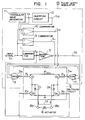
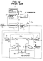
- Fig. 12 shows the arrangement of a conventional pulse-width modulator and driving unit which employs it to drive the actuator
- Fig. 13 is a waveform diagram of waveforms at each portion of the arrangement of Fig. 12.
- an input signal S1 is supplied to a comparator 1 and to an absolute value circuit 2.
- the comparator 1 discriminates the polarity of the input signal S1 to produce a digital signal S2 which is, as shown in Fig. 13, level "H” when the signal S1 is positive (+) relative to the reference level “0” and is level “L” when it is negative (-).
- This signal S2 is supplied to an invertor 3 to produce therefrom a signal S3 which is the inversion of the signal S2.
- the absolute value circuit 2 is used to produce the absolute value of the input signal S1. As shown in Fig. 13 at S4, the absolute value circuit produces the signal S1 when the signal S1 is positive, and it produces the inversion of the signal S1 relative to the "0" level, or the absolute value signal S4.
- This signal S4 is supplied to the non-inverting input terminal of a comparator 4.
- To the inverting input terminal thereof is supplied a triangular wave signal S5 of a high frequency (several tens of kHz to several hundreds of kHz) which rises from the "0" level, and which is produced from a triangular wave generation circuit 5.
- the signals S2, S3, S7 and S8 are supplied to a switching circuit 8.
- the emitters of PNP transistors Q1 and Q2 are connected to a power supply Vcc, while the emitters of NPN transistors Q3 and Q4 are grounded.
- the collectors of the transistors Q1 and Q3 are connected to a terminal 18a of an actuator 18,and the collectors of the transistors Q2 and Q4 to a terminal 18b thereof.
- a flywheel diode D1 has its anode grounded and its cathode connected to the terminal 18a.
- a flywheel diode D2 has its anode grounded and its cathode connected to the terminal 18b.
- the signal S7 is supplied to the base of the transistor Q1 through a resistor R1, the signal S8 is supplied to the base of the transistor Q2 through a resistor R2, the signal S2 is supplied to the base of the transistor Q4 through a resistor R3, and the signal S2 is supplied to the base of the transistor Q4 through a resistor R4.
- these transistors make the ideal operation in which the on-resistance is 0 ⁇ and the off-resistance is ⁇ .
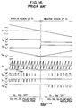
- Fig. 16 is a waveform diagram of waveforms at each portions of the arrangement of Fig. 12 in the case where the signal S5 has an off-set voltage Vof1 in the positive direction.
- the signal S4 when the signal S4 is lower than the voltage Vof1, the signal S6 is always "L” and the two pulse-width modulated signals S7 and S8 are "H".
- the insensitive zone in which no pulse occurs is caused, so that the transistors Q1 and Q2 are in the off-state, thus no current Ia being flowed. Therefore, the current Ia with respect to the signal S1 has the insensitive zone, Vdz as shown in Fig. 17.
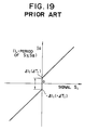
- Fig. 18 is a waveform diagram of waveforms at each portions of the arrangement of Fig. 12 in the case where the signal S5 has an off-set voltage Vof2 in the negative direction. Referring to this figure, even when the signal S4 reaches "0" level, the signal S4 is larger than the minimum level of the signal S5. At this time, the signal S6 becomes "H” only for the period, ⁇ T corresponding to the off-set voltage Vof2.
- the pulse-width modulated signal S7 or S8 may have such pulse width ("L" period ) as to discontinuously skip not via "0" as ⁇ T ⁇ - ⁇ T or - ⁇ T ⁇ ⁇ T (it is assumed that the pulse width of "L" level of signal S7 is represented by +, and that the pulse width of "L” level of signal S8 is denoted by -) (hereinafter, this skip characteristic is called the discontinuous characteristic ).
- the "L" period of the signal S7 or S8 relative to the signal S1 is longer than in the case of Fig. 13.
- the drive current Ia vs signal S1 characteristic is as shown in Fig. 19, that is, the current Ia is discontinuously changed at around "0" of signal S1 as + ⁇ I1 ⁇ - ⁇ I1.
- the comparator 4 has a response time in which the triangular wave signal S5 and the absolute value signal S4 are compared with each other, this response time being another factor which causes the discontinuous characteristic and the insensitive zone. If the relation between the rise time, tr and fall time tf of this comparator is tr > tf, the "L" period of the signal S6 becomes short, thus causing the insensitive zone in the pulse-width modulated signals S7 and S8 as in Fig. 16 and also the insensitive zone in the characteristic of the drive current with respect to the input signal S1. On the contrary, if tf > tr, the "L" period of the signal S6 becomes long, so that the discontinuous characteristic is caused in the relation of the input signal to the pulse-width modulated signals S7 and S8 or to the drive current.
- the conventional pulse-width modulator has the drawback that the insensitive zone and the discontinuous characteristic are easy to be caused by the off-set of the triangular wave signal and the response time of the comparator, making the pulse-width modulated signal erroneous.
- the driving unit using this modulator is similarly easy to produce the insensitive zone and the discontinuous characteristic, so that it is impossible to obtain a correct drive current proportional to the input signal.
- the triangular wave signal rising from the "0" level, or the off-set is easy to occur as shown in Figs. 16 and 18. Also, since the frequency of the triangular wave signal is normally as high as several tens of kHz to several hundreds of kHz, it is difficult to realize a comparator which can operate at so high a frequency that the period can be neglected.
- the insensitive zone and the discontinuous characteristic becomes great, making it further difficult to operate the pulse-width modulator and the driving unit using it with high precision.
- EP-A-0 100 103 discloses a pulse width modulation circuit capable of cancelling the mean error of pulse width modulation with respect to time, due to the offset voltage of a triangular wave signal and to the offset voltage of a comparator. Circuits are added to an existing pulse width modulation circuit used in an integration circuit forming the product of two analog signals. The offset of a triangular weave signal is cancelled by inverting either the triangular wave signal with respect to the input signal or the input signal with respect to the triangular wave signal, in every predetermined period. The offset of a comparator is eliminated by inverting the output of the comparator and replacing the input terminals of the comparator if the input signal is not inverted, or by connecting the input terminal of the comparator as such, if the input signal is inverted.
- the invention enables the insensitive zone and the discontinuous characteristic to be avoided in the relationships between the input signal and either the pulse-width of the pulse-width modulated signal or the drive current Ia. Hence a correct pulse-width modulated signal can be produced. That is, the pulse-width modulator can operate precisely, and the driving unit using it can operate with high accuracy and small power consumption.
- this invention is applied to the actuator driving circuit or the like of optical recording and/or reproducing apparatus, the power consumption in the apparatus is small, and the insensitive zone can be prevented from occurring to deteriorate the control precision or the discontinuity characteristic can be prevented from occurring to make the control system unstable.
- Fig. 1 shows an arrangement of one embodiment of a pulse-width modulator and driving unit using the same according to this invention
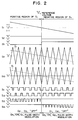
- Fig. 2 is a waveform diagram of waves at each portions of the arrangement of Fig. 1.
- like elements corresponding to those in the conventional example are indentified by the same reference numerals.
- a pulse-width modulator 19 which includes the comparator 1, the invertor 3, a comparator 9, a comparator 10, a triangular wave generation circuit 11, an inverting circuit 12, a NAND gate 13, and a NOR gate 14.
- This pulse-width modulator 19 and the switching circuit 8 constitute a driving unit.
- the input signal S1 is supplied to the comparator 1, the non-inverting input end of the comparator 9 and the inverting input end of the comparator 10.
- the comparator 1 and the invertor 3 respectively produce the signals S2 and S3 for discriminating the polarity of the input signal S1 as in the conventional example of Fig. 12.
- the comparator 9 is also supplied at its inverting input end with the first triangular wave signal S9 which, as shown in Fig. 2 is substantially symmetrical with respect to the "0" level, from the triangular wave generation circuit 11.
- This signal S9 is also supplied to the inverting circuit 12 to produce therefrom a second triangular wave signal S10 (hereinafter, called the inverted triangular wave signal) resulting from inverting the signal S9 relative to the "0" level, as shown in Fig. 2.
- This signal S10 is supplied to the non-inverting input end of the comparator 10.
- the comparator 9 produces a digital signal S11 of level "H”.
- the comparator 10 produces a digital signal S12 of level "H".
- the signal S11 has equal durations of "H” and “L” when the signal S1 is “0” level, increases the duration of “H” when the signal S1 is positive and increases, and decreases the duration of "H” when the signal S1 is negative and decreases.
- the signal S12 has equal duration of "H” and “L” when the signal S1 is “0”, decreases the duration of “H” when the signal S1 is positive and increases, and increases the duration of "H” when the signal S1 is negative and decreases.
- the signals S11 and S12 are two pulse-width modulated signals with different phases of which the pulse widths change in the opposite directions with the change of the input signal S1, and become equal when the input signal S1 is "0" level.
- the pulse-width modulator according to this invention produces such two pulse-width modulated signals of different phases as the signals S11 and S12 relative to the input signal,and further produces a differential pulse-width modulated signal which is the difference between the pulse widths of the two signals of different phases.
- This differential pulse-width modulated signal is used as the actual modulated signal.
- the signals S11 and S12 are, respectively, supplied to the NAND gate 13 with an inverting input end and the NOR gate 14 with an inverting input end.
- the NAND gate 13 produces a signal S13 which, as shown in Fig. 2, has “L” level when the signals S11 and S12 are,respectively, “H” and “L”, or in the period corresponding to the difference between the pulse widths of "H” of the signals S11 and S12.
- the NOR gate 14 produces a signal S14 which, as shown in Fig. 2, has “L” level when the signals S11 and S12 are, respectively, “L” and “H”, or in the period corresponding to the difference between the pulse widths of "L” of the signals S11 and S12.
- the signals S13 and S14 have the pulse widths of "L" modulated.
- the signal S13 has the pulse width proportional to the signal S1 when the input signal S1 is positive, but no pulse when the signal S1 is negative, that is, the signal S13 is a pulse-width modulated signal only for the positive region of the input signal.
- the signal S14 has the pulse width proportional to the negative level of the signal S1 when the signal S1 is negative, but no pulse when the signal S1 is positive, that is, the signal S14 is a pulse-width modulated signal only for the negative region of the input signal.
- the signal S13 has the pulse width of "L” level when the input signal S1 is larger than the triangular wave signal S9 and larger than the inverted triangular wave signal S10.
- the signal S14 has the pulse width of "L” level when the input signal S1 is smaller than the triangular wave signal S9 and smaller than the inverted triangular wave signal S10.
- the signals S13 and S14 and the signals S2 and S3 are supplied to the same switching circuit 8 as shown in Fig. 12.
- the signal S3 is supplied to the base of the transistor Q3 through the resistor R3, the signal S2 to the base of the transistor Q4 through the resistor R4, the signal S13 to the base of the transistor Q1 through the resistor R1, and the signal S14 to the base of the transistor Q2 through the resistor R2.
- the signal S1 is positive
- the transistors Q2 and Q3 are both in the off-state and the transistor Q4 is in the on-state, thus, the switching circuit 8 corresponding to the equivalent circuit of Fig. 14a in which the signal S7 is replaced by signal S12.
- the current Ia flowing in the actuator 18 is proportional to the input signal S1 as in Fig. 15.
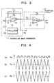
- the triangular wave signal S9 and the inverted triangular wave signal S10 can be produced from the circuit shown in Fig. 3.
- Figs. 4a, 4b and 4c show waveforms at each portions of the arrangement of Fig. 3.
- an oscillator 15 produces a rectangular wave signal S15 of equal durations of "H" and "L", or 50-% duty factor.
- This signal is supplied through a capacitor C1, so that the DC voltage is removed from the signal S15.
- the signal from the capacitor is supplied to a well-known Miller integration circuit which is formed of an operational amplifier 16, resistors R5 and R6 and a capacitor C2.
- the Miller integration circuit produces the triangular wave signal S9 which rises in the "L” period of the signal S15 and falls in the "H” period thereof.
- the signal S9 is supplied to the inversion circuit 12 which is formed of an operational amplifier 17 and resistors R7 and R8.
- the inverting circuit produces the inverted triangular signal S10.
- the off-set in the operational amplifier is normally very low and easy to be suppressed to, for example, 1 mv or below. Therefore, the inverting circuit 12 is able to invert the signal S9 precisely with a small off-set relative to the "0" level (which is the potential of ground in Fig. 3).
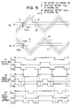
- FIG. 5 shows the waveform for the positive voltage of the signal S1.
- the solid line indicates the waveform of the signal S9 with no off-set
- the one-dot chain line indicates the waveform of the signal S9 with an off-set voltage of only Vof1 in the positive direction
- the broken line indicates the waveform of the signal S9 with an off-set voltage of only Vof2 in the negative direction.
- Fig. 5 shows the waveform for the positive voltage of the signal S1.
- I indicates the waveform of the signal S9 with no off-set
- the one-dot chain line indicates the waveform of the signal S9 with an off-set voltage of only Vof1 in the positive direction
- the broken line indicates the waveform of the signal S9 with an off-set voltage of only Vof2 in the negative direction.
- the solid line indicates the waveform of the signal S10 in the case where the signal S9 has no off-set
- the one-dot chain line indicates the waveform of the signal S10 in the case where the signal S9 has only Vof1 in the positive direction
- the broken line indicates the waveform of the signal S10 in the case direction,and where the signal S9 has an off-set of only Vof2 in the negative direction.
- the lines I, II, III indicate the same as those in Fig. 5.
- the off-set voltage is also inverted by the inverting circuit 12 so that the signal S10 has an off-set voltage of Vof1 in the opposite direction to the signal S9,or in the negative direction.
- the signal S9 is as indicated by the broken line III, the signal S10 has an off-set voltage of Vof2 in the opposite direction to the signal S9, or in the positive direction. Therefore, the signals S11, S12 and S13 have such waveforms as shown by I, II, III, on the lower side of Fig. 5.
- the modulated signal S13 for each case is not changed in the pulse width of "L” level but is only shifted in the time base of the "L” period indicated by the arrows.
- the signal S14, though not shown is always of "H” level.
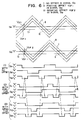
- Fig. 6 shows the waveforms relative to the signal S1 of negative voltage.
- the modulated signal S13 for each case I, II, III is not changed in the pulse width but is only shifted in the time base as indicated by the arrows.
- the signal S14, though not shown is always of "H" level.
- Fig. 7 shows the waveforms relative to the signal S1 of "0" level.
- the modulated signals S13 and S14 are always of "H” level.
- the pulse widths of the modulated signals S13 and S14 and the drive current Ia are not changed by the off-set of the triangular wave signal S9, but are proportional to the input signal, and there are not produced such insensitive zone and the discontinuous characteristic as in the prior art.
- the comparators 9 and 10 in Fig. 1 can be constructed in the same circuit, and the response times such as tr and tf can be achieved to be close. Particularly, when these circuits are formed in the same integrated circuit chip, most characteristics including the response time, of the circuits are extremely similar.
- the comparators 9 and 10 are formed close to each other and in the same shape to be preferably of the same circuit construction on one integrated circuit chip so that the response times (tr, tf) are extremely close to each other, then the pulse widths of the pulse-width modulated signals and the drive current Ia are not affected by the response times (tr, tf), but are proportional to the input signal.
- Fig. 9 shows the arrangement of another embodiment of a pulse-width modulator and driving unit using the same according to this invention.
- Fig. 10 is a waveform diagram of waves at each portions of the arrangement of Fig. 9.
- like elements as those in the conventional example or in Figs. 1 and 2 are identified by the same reference numerals and characters.
- the comparator 1, the invertor 3, the triangular wave generation circuit 11, the comparator 9, the comparator 10, an inverting circuit 20, the NAND gate 13, and the NOR gate 14 constitute a pulse-width modulator 19′.
- This pulse-width modulator 19′ and the switching circuit 8 constitute a driving unit.
- the input signal S1 is supplied to the comparator 1, the non-inverting input end of the comparator 9, and the inverting circuit 20.
- the triangular wave signal S9 from the triangular wave generation circuit 11 is supplied to the inverting input end of the comparator 9 and the inverting input end of the comparator 10.
- the comparator 1 and the invertor 3 produce the signals S2 and S3 for discriminating the polarity of the input signal S1 in the same way as in Fig. 2.
- the inverting circuit 20 inverts the input signal S1 relative to "0" level to produce an input inverted signal S16. This signal S16 is supplied to the non-inverting input end of the comparator 10.
- the comparator 9 compares the levels of the signal S9 and the input signal S1 to produce the signal S11 which becomes “H” when the input signal S1 is larger than the triangular wave signal S9, as in Fig. 2.
- the comparator 10 compares the levels of the triangular wave signal S9 and the input inverted signal S16 to produce a signal S12′ which becomes "H” when the signal S16 is larger than the signal S9.
- Fig. 9 The arrangement of Fig. 9 is different from that of Fig. 1 in that the signals to be compared are different in the respective comparators 10.
- the input signal S1 is supplied to the inverting input end of the comparator 10 and the signal S10 resulting from inverting the triangular wave signal S9 is supplied to the non-inverting input thereof, so that the output signal S12 is produced therefrom as a result of level comparison.
- the input inverted signal S16 resulting from inverting the input signal S1 is supplied to the non-inverting end of the comparator 10 and the triangular wave signal S9 is supplied to the inverting input end thereof, so that the output signal S12′ is produced therefrom.
- the signals S11 and S12′ produced from the comparators 10 are equivalent.
- the signals S11 and S12′ are, respectively supplied to the inverting input ends of the NAND gate 13 and NOR gate 14 in the same way as in Fig. 1.
- the output signals S13′, S14′ are equivalent to the signals S13, S14 shown in Fig. 2.
- the signal S13′ has a pulse "L” level in the period in which the input signal S1 is larger than the triangular wave signal S9 and the input inverted signal S16 is smaller than the signal S9.
- the signal S14′ has a pulse width of "L” level in the period in which the input signal S1 is smaller than the triangular wave signal S9 and the input inverted signal S16 is larger than the triangular wave signal S9.
- the signals S13′, S14′, S2 and S3 are supplied to the same switching circuit 8 as shown in Fig. 1.
- the signal S2 is supplied through the resistor R4 to the base of the transistor Q4
- the signal S3 is supplied through the resistor R3 to the base of the transistor Q3
- the signal S13′ is supplied through the resistor R1 to the base of the transistor Q1
- the signal S14′ is supplied through the resistor R2 to the base of the transistor Q2.
- Fig. 9 can provide a pulse-width modulator and driving unit using the same which are able to properly operate without the effect of the off-set of the triangular wave signal S9 and the response times of the comparator 9 and the comparator 10 similarly to the arrangement of Fig. 1.
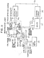
- Fig. 11 is a block diagram of the focus control system of an optical recording and reproducing apparatus in which the control unit of this invention is used.
- a disc like recording medium 21 is placed on a turntable 22 and fixed not to slip against each other by a disc clamp 23.
- the turntable 22 is directly driven by the rotating shaft, 24 of a disc motor 25 so that the disc-like recording medium 21 is rotated at a predetermined rate.
- laser light 27 emitted from a semiconductor laser 26 is shaped into parallel light by a collimator lens 28, passed through a deflection beam splitter 29, and focused by an object lens 30 into a light spot on the disc-like recording medium 21.
- the disc-like recording medium 21 has surface fluctuation, by which the relative position of the object lens 30 to the disc-like recording medium is changed while the medium is rotating under the condition that the object lens is fixed in position. This follows that the light spot on the disc-like recording medium 21 is defocused, thus failing to make recording or reproducing.
- the object lens 30 is required to be changed in position to follow the positional change of the disc-like recording medium 21 due to the surface fluctuation or the like, and thereby to control the light spot to always be focused on the disc-like recording medium by means of a focusing controller.
- This focus detection optical system 31 may use, for example, a known knife edge method which comprises a detection lens 32, a shielding plate 33 having a knife edge placed near the detection lens 33, and a double-portion light detector 34 for detecting the light passed this shielding plate.
- This double-portion light detector 34 is formed of two light detectors 34a and 34b. When the light spot is in focus, the amount of light incident to each of the two detectors 34a and 34b is equal.
- the amount of light spot on the detector 34a increases, while the amount of the light spot on the detector 34b decreases.
- the amount of the light spot on the detector 34a decreases, while that on the detector 34b increases.
- the detectors 34a, 34b produce photocurrents Ip1, Ip2 of which the intensity is proportional to the amount of the light irradiation, and supply them to a detection circuit 35.
- This detection circuit produces a focus error signal S17 corresponding to the difference therebetween.
- This focus error signal 17 is supplied to a control circuit 36, which amplifies or phase-compensates the input signal if necessary, to produce the signal S1.
- This signal S1 is supplied to a driver 37.
- the driver 37 is constructed as in Fig. 1 or 9, and its output terminals 18a and 18b are connected to the actuator 18.
- the actuator 18 permits the object lens 30 to move in the direction perpendicular to the surface of the disc-like recording medium 21 in which case the displacement is proportional to the drive current Ia.
- the actuator is controlled in its amount of displacement in accordance with the intensity of the signal so that the focus error signal S17 is always zero.
- the distance between the object lens 30 and the disc-like recording medium 21 is constant, and thus the light spot is focused on the surface of the disc-like recording medium.
- the optical-type recording and/or reproducing apparatus requires not only this focus control system but also the tracking control system for permitting the light spot to trace the information track with high precision, or a traverse control system for permitting the whole optical head to move.
- each control system needs the actuator and the driver.
- the driving unit according to this invention can be applied not only to the driving of the actuator of the optical-type recording and/or reproducing apparatus but also to, for, example, an acoustic-purpose power amplifier for driving a loud speaker. In other words, the driving unit can be applied to the system which requires small size, power saving and has high precision.
Landscapes
- Inverter Devices (AREA)
- Optical Recording Or Reproduction (AREA)
- Feedback Control In General (AREA)
- Control Of Position Or Direction (AREA)
Claims (2)
- Pulsbreitenmodulationssystem mit:
einer Dreieckswellenerzeugungseinrichtung (11) zur Erzeugung eines ersten Dreieckswellensignals (S9);
einer Invertereinrichtung (12) zur Erzeugung eines zweiten Dreieckswellensignals (S10), das zu dem ersten Dreieckswellensignal (S9) bezogen auf eine daran angelegte Bezugsspannung in einer umgekehrten Beziehung steht;
einer ersten Vergleichereinrichtung (9) zum Vergleichen eines Eingangssignals (S1) mit dem ersten Dreieckswellensignal (S9), um ein erstes Pulsbreitenmodulationssignal (S11) zu bilden;
einer zweiten Vergleichereinrichtung (10) zum Vergleichen des Eingangssignals (S1) mit dem zweiten Dreieckswellen-Signal (S10), um ein zweites Pulsbreitenmodulationssignal (S12) zu bilden;
einer ersten Verknüpfungsgliedeinrichtung (13) zum Empfangen des ersten und des zweiten Pulsbreitenmodulationssignals von der ersten und der zweiten Vergleichereinrichtung;
einer zweiten Verknüpfungsgliedeinrichtung (14) zum Empfangen des ersten und des zweiten Pulsbreitenmodulationssignals von der ersten und der zweiten Vergleichereinrichtung;
dadurch gekennzeichnet, daß:
die erste Verknüpfungsgliedeinrichtung (13) ein erstes Differenzpulsbreitenmodulationssignal (S13) aus einer Differenz zwischen pulsbreiten des ersten und des zweiten Pulsbreitenmodulationssignals (S11, S12), wenn das Eingangssignal positiv in bezug auf die Bezugsspannung ist, erzeugt, und die zweite Verknüpfungsgliedeinrichtung (14) ein zweites Differenzpulsbreitenmodulationssignal (S14) aus einer Differenz zwischen Pulsbreiten des ersten und des zweiten Pulsbreitenmodulationssignals (S11, S12), wenn das Eingangssignal negativ in bezug auf das Bezugssignal ist, erzeugt; und
das erste und das zweite Pulsbreitenmodulationssignal (S13, S14) vorgesehen sind, um den Ein-Zustand eines ersten und eines zweiten Transistors (Q1, Q2) eines Schalterkreises zu steuern. - Pulsbreitenmodulationssystem nach Anspruch 1, dadurch gekennzeichnet, daß die erste Vergleichereinrichtung (9) zur Erzeugung des ersten Pulsbreitenmodulationssignals (S11) und die zweite Vergleichereinrichtung (10) zur Erzeugung des zweiten pulsbreitenmodulationssignals (S12) in derselben Schaltkreisanordnung in einem integrierten Schaltkreischip ausgebildet sind.
Applications Claiming Priority (2)
| Application Number | Priority Date | Filing Date | Title |
|---|---|---|---|
| JP184386/88 | 1988-07-22 | ||
| JP18438688 | 1988-07-22 |
Publications (3)
| Publication Number | Publication Date |
|---|---|
| EP0352137A2 EP0352137A2 (de) | 1990-01-24 |
| EP0352137A3 EP0352137A3 (en) | 1990-08-22 |
| EP0352137B1 true EP0352137B1 (de) | 1994-11-30 |
Family
ID=16152277
Family Applications (1)
| Application Number | Title | Priority Date | Filing Date |
|---|---|---|---|
| EP89307461A Expired - Lifetime EP0352137B1 (de) | 1988-07-22 | 1989-07-21 | Pulsbreitenmodulator und Treiberschaltung mit diesem Modulator |
Country Status (4)
| Country | Link |
|---|---|
| US (1) | US5030847A (de) |
| EP (1) | EP0352137B1 (de) |
| JP (1) | JPH02125302A (de) |
| DE (1) | DE68919568T2 (de) |
Families Citing this family (8)
| Publication number | Priority date | Publication date | Assignee | Title |
|---|---|---|---|---|
| US5200648A (en) * | 1991-08-13 | 1993-04-06 | National Semiconductor Corporation | Emulator circuit and method for generating CMOS level clock input |
| KR100672096B1 (ko) * | 1998-12-30 | 2007-01-19 | 코닌클리즈케 필립스 일렉트로닉스 엔.브이. | 다상 d.c. 모터의 구동 장치, 다상 d.c. 모터를 포함하는 구동 시스템 및 디스크 드라이브 |
| JP3591519B2 (ja) * | 2002-02-22 | 2004-11-24 | オンキヨー株式会社 | パルス幅変調回路 |
| RU2216850C1 (ru) * | 2002-02-26 | 2003-11-20 | Государственное образовательное учреждение высшего профессионального образования Самарский государственный технический университет | Цифровой модулятор для преобразователя частоты асинхронного электродвигателя |
| RU2231205C1 (ru) * | 2002-10-10 | 2004-06-20 | Открытое акционерное общество "Федеральная сетевая компания Единой энергетической системы" | Способ управления преобразователем напряжения |
| RU2517423C1 (ru) * | 2012-11-07 | 2014-05-27 | Федеральное государственное бюджетное образовательное учреждение высшего профессионального образования Самарский государственный технический университет | Цифровой модулятор для управления синхронным электродвигателем |
| RU2711049C1 (ru) * | 2019-01-10 | 2020-01-14 | федеральное государственное бюджетное образовательное учреждение высшего образования "Самарский государственный технический университет" | Цифровой модулятор для управления синхронным двигателем |
| US11085532B2 (en) * | 2019-03-12 | 2021-08-10 | GM Global Technology Operations LLC | Method for controlling a hydraulic system |
Family Cites Families (8)
| Publication number | Priority date | Publication date | Assignee | Title |
|---|---|---|---|---|
| US3260912A (en) * | 1963-06-19 | 1966-07-12 | Gen Motors Corp | Power amplifier employing pulse duration modulation |
| US3551851A (en) * | 1968-05-27 | 1970-12-29 | Westinghouse Electric Corp | Class a-b pulse width modulating amplifiers |
| US3743911A (en) * | 1971-06-18 | 1973-07-03 | Gen Electric | Servomotor pulse width control circuit capable of compensating for variations in supply voltage |
| JPS513161A (de) * | 1974-06-25 | 1976-01-12 | Nippon Denso Co | |
| DE2452120A1 (de) * | 1974-11-02 | 1976-05-13 | Michael Ing Grad Moege | Anordnung zur verstaerkung und uebertragung analoger signale mit digitalen logikelementen und schaltverstaerkern, bei denen die signaluebertragung und verwertung in 2 parallelen zweigen erfolgt |
| JPS5922441A (ja) * | 1982-07-28 | 1984-02-04 | Hitachi Ltd | デジタル出力型積分回路 |
| JPS60190010A (ja) * | 1984-03-12 | 1985-09-27 | Sony Corp | パルス幅変調信号による制御回路 |
| JPS61116107A (ja) * | 1984-11-09 | 1986-06-03 | Hitachi Ltd | アクチユエ−タの制御装置 |
-
1989
- 1989-06-12 JP JP1148983A patent/JPH02125302A/ja active Pending
- 1989-07-19 US US07/381,940 patent/US5030847A/en not_active Expired - Lifetime
- 1989-07-21 DE DE68919568T patent/DE68919568T2/de not_active Expired - Fee Related
- 1989-07-21 EP EP89307461A patent/EP0352137B1/de not_active Expired - Lifetime
Also Published As
| Publication number | Publication date |
|---|---|
| DE68919568T2 (de) | 1995-04-13 |
| EP0352137A2 (de) | 1990-01-24 |
| EP0352137A3 (en) | 1990-08-22 |
| JPH02125302A (ja) | 1990-05-14 |
| US5030847A (en) | 1991-07-09 |
| DE68919568D1 (de) | 1995-01-12 |
Similar Documents
| Publication | Publication Date | Title |
|---|---|---|
| EP0183849B1 (de) | Steuerschaltungen die mit impulsbreiten, modulierten signalen arbeiten | |
| US5444682A (en) | Tracking control apparatus | |
| US5231280A (en) | Focusing error detection apparatus using a first and second knife edge at different positions | |
| US4748610A (en) | Servo system in data reading apparatus | |
| CA1213046A (en) | Servo apparatus and flaw detecting apparatus therefor for optical disc player | |
| US4787078A (en) | Optical data recording and reproducing system with control of high frequency superposed signal applied to semiconductor laser | |
| EP0362938B1 (de) | Anordnung zum Abtasten eines Aufzeichnungsträgers sowie Regelschaltung zum Anwenden in einer derartigen Anordnung | |
| EP0352137B1 (de) | Pulsbreitenmodulator und Treiberschaltung mit diesem Modulator | |
| EP0289309B1 (de) | Gerät zur Wiedergabe einer optischen Platte | |
| US4718068A (en) | Stabilized laser device of optical information recording/reproduction apparatus | |
| US4512003A (en) | Control circuitry for preliminary focusing of light on a record medium surface in an optical reproducing apparatus | |
| JPH02166636A (ja) | レーザ駆動回路 | |
| US5574707A (en) | Pulse width control apparatus for optical disk | |
| US6459315B2 (en) | Wave reforming circuit | |
| US4631712A (en) | Optical disk apparatus with beam energy correction for deviations in inclination | |
| US5161243A (en) | Tracking system for an optical recording/reproducing apparatus having a plurality of light spots | |
| EP0654785B1 (de) | Fehlerkorrekturgerät mit Mitteln zum Halten eines Fehlerkorrektursignals | |
| EP0373607B1 (de) | Fokusfehlerermittlungsschaltung | |
| US5107135A (en) | Sinusoidal-to-squarewave converter with variable thereshold level | |
| EP0555865B1 (de) | Servospurfolgekreis für Gerät für optische Scheiben | |
| US5570009A (en) | Constant-Current circuitry, IC device driver using same, and unit using the device | |
| JP3633635B2 (ja) | 記録担体走査デバイス | |
| US4811194A (en) | Optical information processing apparatus | |
| KR940005101B1 (ko) | 광학 판독 레코드 캐리어상의 광빔 주사용 장치 | |
| JPS592235A (ja) | 光学式情報読取装置におけるサ−ボ装置 |
Legal Events
| Date | Code | Title | Description |
|---|---|---|---|
| PUAI | Public reference made under article 153(3) epc to a published international application that has entered the european phase |
Free format text: ORIGINAL CODE: 0009012 |
|
| AK | Designated contracting states |
Kind code of ref document: A2 Designated state(s): DE FR GB NL |
|
| PUAL | Search report despatched |
Free format text: ORIGINAL CODE: 0009013 |
|
| AK | Designated contracting states |
Kind code of ref document: A3 Designated state(s): DE FR GB NL |
|
| 17P | Request for examination filed |
Effective date: 19901011 |
|
| 17Q | First examination report despatched |
Effective date: 19920917 |
|
| GRAA | (expected) grant |
Free format text: ORIGINAL CODE: 0009210 |
|
| AK | Designated contracting states |
Kind code of ref document: B1 Designated state(s): DE FR GB NL |
|
| REF | Corresponds to: |
Ref document number: 68919568 Country of ref document: DE Date of ref document: 19950112 |
|
| ET | Fr: translation filed | ||
| PLBE | No opposition filed within time limit |
Free format text: ORIGINAL CODE: 0009261 |
|
| STAA | Information on the status of an ep patent application or granted ep patent |
Free format text: STATUS: NO OPPOSITION FILED WITHIN TIME LIMIT |
|
| 26N | No opposition filed | ||
| PGFP | Annual fee paid to national office [announced via postgrant information from national office to epo] |
Ref country code: FR Payment date: 20000711 Year of fee payment: 12 |
|
| PGFP | Annual fee paid to national office [announced via postgrant information from national office to epo] |
Ref country code: DE Payment date: 20000717 Year of fee payment: 12 |
|
| PGFP | Annual fee paid to national office [announced via postgrant information from national office to epo] |
Ref country code: GB Payment date: 20000719 Year of fee payment: 12 |
|
| PGFP | Annual fee paid to national office [announced via postgrant information from national office to epo] |
Ref country code: NL Payment date: 20000728 Year of fee payment: 12 |
|
| PG25 | Lapsed in a contracting state [announced via postgrant information from national office to epo] |
Ref country code: GB Free format text: LAPSE BECAUSE OF NON-PAYMENT OF DUE FEES Effective date: 20010721 |
|
| PG25 | Lapsed in a contracting state [announced via postgrant information from national office to epo] |
Ref country code: NL Free format text: LAPSE BECAUSE OF NON-PAYMENT OF DUE FEES Effective date: 20020201 |
|
| GBPC | Gb: european patent ceased through non-payment of renewal fee |
Effective date: 20010721 |
|
| PG25 | Lapsed in a contracting state [announced via postgrant information from national office to epo] |
Ref country code: FR Free format text: LAPSE BECAUSE OF NON-PAYMENT OF DUE FEES Effective date: 20020329 |
|
| NLV4 | Nl: lapsed or anulled due to non-payment of the annual fee |
Effective date: 20020201 |
|
| PG25 | Lapsed in a contracting state [announced via postgrant information from national office to epo] |
Ref country code: DE Free format text: LAPSE BECAUSE OF NON-PAYMENT OF DUE FEES Effective date: 20020501 |
|
| REG | Reference to a national code |
Ref country code: FR Ref legal event code: ST |