EP0349910A2 - Procédé pour la fabrication de couches minces supraconductrices à haute température contenant de l'oxyde - Google Patents
Procédé pour la fabrication de couches minces supraconductrices à haute température contenant de l'oxyde Download PDFInfo
- Publication number
- EP0349910A2 EP0349910A2 EP89111892A EP89111892A EP0349910A2 EP 0349910 A2 EP0349910 A2 EP 0349910A2 EP 89111892 A EP89111892 A EP 89111892A EP 89111892 A EP89111892 A EP 89111892A EP 0349910 A2 EP0349910 A2 EP 0349910A2
- Authority
- EP
- European Patent Office
- Prior art keywords
- layers
- temperature
- substrate surface
- substrate
- mbar
- Prior art date
- Legal status (The legal status is an assumption and is not a legal conclusion. Google has not performed a legal analysis and makes no representation as to the accuracy of the status listed.)
- Withdrawn
Links
Images

Classifications
-
- C—CHEMISTRY; METALLURGY
- C23—COATING METALLIC MATERIAL; COATING MATERIAL WITH METALLIC MATERIAL; CHEMICAL SURFACE TREATMENT; DIFFUSION TREATMENT OF METALLIC MATERIAL; COATING BY VACUUM EVAPORATION, BY SPUTTERING, BY ION IMPLANTATION OR BY CHEMICAL VAPOUR DEPOSITION, IN GENERAL; INHIBITING CORROSION OF METALLIC MATERIAL OR INCRUSTATION IN GENERAL
- C23C—COATING METALLIC MATERIAL; COATING MATERIAL WITH METALLIC MATERIAL; SURFACE TREATMENT OF METALLIC MATERIAL BY DIFFUSION INTO THE SURFACE, BY CHEMICAL CONVERSION OR SUBSTITUTION; COATING BY VACUUM EVAPORATION, BY SPUTTERING, BY ION IMPLANTATION OR BY CHEMICAL VAPOUR DEPOSITION, IN GENERAL
- C23C14/00—Coating by vacuum evaporation, by sputtering or by ion implantation of the coating forming material
- C23C14/22—Coating by vacuum evaporation, by sputtering or by ion implantation of the coating forming material characterised by the process of coating
- C23C14/24—Vacuum evaporation
- C23C14/28—Vacuum evaporation by wave energy or particle radiation
-
- C—CHEMISTRY; METALLURGY
- C23—COATING METALLIC MATERIAL; COATING MATERIAL WITH METALLIC MATERIAL; CHEMICAL SURFACE TREATMENT; DIFFUSION TREATMENT OF METALLIC MATERIAL; COATING BY VACUUM EVAPORATION, BY SPUTTERING, BY ION IMPLANTATION OR BY CHEMICAL VAPOUR DEPOSITION, IN GENERAL; INHIBITING CORROSION OF METALLIC MATERIAL OR INCRUSTATION IN GENERAL
- C23C—COATING METALLIC MATERIAL; COATING MATERIAL WITH METALLIC MATERIAL; SURFACE TREATMENT OF METALLIC MATERIAL BY DIFFUSION INTO THE SURFACE, BY CHEMICAL CONVERSION OR SUBSTITUTION; COATING BY VACUUM EVAPORATION, BY SPUTTERING, BY ION IMPLANTATION OR BY CHEMICAL VAPOUR DEPOSITION, IN GENERAL
- C23C14/00—Coating by vacuum evaporation, by sputtering or by ion implantation of the coating forming material
- C23C14/06—Coating by vacuum evaporation, by sputtering or by ion implantation of the coating forming material characterised by the coating material
- C23C14/08—Oxides
- C23C14/087—Oxides of copper or solid solutions thereof
-
- C—CHEMISTRY; METALLURGY
- C23—COATING METALLIC MATERIAL; COATING MATERIAL WITH METALLIC MATERIAL; CHEMICAL SURFACE TREATMENT; DIFFUSION TREATMENT OF METALLIC MATERIAL; COATING BY VACUUM EVAPORATION, BY SPUTTERING, BY ION IMPLANTATION OR BY CHEMICAL VAPOUR DEPOSITION, IN GENERAL; INHIBITING CORROSION OF METALLIC MATERIAL OR INCRUSTATION IN GENERAL
- C23C—COATING METALLIC MATERIAL; COATING MATERIAL WITH METALLIC MATERIAL; SURFACE TREATMENT OF METALLIC MATERIAL BY DIFFUSION INTO THE SURFACE, BY CHEMICAL CONVERSION OR SUBSTITUTION; COATING BY VACUUM EVAPORATION, BY SPUTTERING, BY ION IMPLANTATION OR BY CHEMICAL VAPOUR DEPOSITION, IN GENERAL
- C23C14/00—Coating by vacuum evaporation, by sputtering or by ion implantation of the coating forming material
- C23C14/58—After-treatment
- C23C14/5806—Thermal treatment
-
- C—CHEMISTRY; METALLURGY
- C23—COATING METALLIC MATERIAL; COATING MATERIAL WITH METALLIC MATERIAL; CHEMICAL SURFACE TREATMENT; DIFFUSION TREATMENT OF METALLIC MATERIAL; COATING BY VACUUM EVAPORATION, BY SPUTTERING, BY ION IMPLANTATION OR BY CHEMICAL VAPOUR DEPOSITION, IN GENERAL; INHIBITING CORROSION OF METALLIC MATERIAL OR INCRUSTATION IN GENERAL
- C23C—COATING METALLIC MATERIAL; COATING MATERIAL WITH METALLIC MATERIAL; SURFACE TREATMENT OF METALLIC MATERIAL BY DIFFUSION INTO THE SURFACE, BY CHEMICAL CONVERSION OR SUBSTITUTION; COATING BY VACUUM EVAPORATION, BY SPUTTERING, BY ION IMPLANTATION OR BY CHEMICAL VAPOUR DEPOSITION, IN GENERAL
- C23C14/00—Coating by vacuum evaporation, by sputtering or by ion implantation of the coating forming material
- C23C14/58—After-treatment
- C23C14/5846—Reactive treatment
- C23C14/5853—Oxidation
-
- H—ELECTRICITY
- H10—SEMICONDUCTOR DEVICES; ELECTRIC SOLID-STATE DEVICES NOT OTHERWISE PROVIDED FOR
- H10N—ELECTRIC SOLID-STATE DEVICES NOT OTHERWISE PROVIDED FOR
- H10N60/00—Superconducting devices
- H10N60/01—Manufacture or treatment
- H10N60/0268—Manufacture or treatment of devices comprising copper oxide
- H10N60/0296—Processes for depositing or forming copper oxide superconductor layers
- H10N60/0521—Processes for depositing or forming copper oxide superconductor layers by pulsed laser deposition, e.g. laser sputtering
Definitions
- the invention relates to a method for producing thin layers of material of an oxide high-temperature superconductor, in which the material is used as the target material in the stoichiometric composition of the superconductor and the layer by removing target material with the aid of a laser and forming a precipitate on a heated substrate is formed.
- the layers are formed under oxygen partial pressure of at least 0.1 mbar at a temperature of the substrate surface in the range between 600 ° C and 900 ° C.
- layers with superconducting properties are formed directly by the method according to the invention, which consists of practically a single process step, whereas, in contrast to this, the superconducting properties only set in the complex aftertreatment in the known method mentioned above.
- the material forming the layer is already enriched with oxygen during laser ablation and the formation of the layers. This means that layers with superconducting properties can be produced directly.
- the partial pressure of the oxygen to be set is limited only by technical secondary conditions, for example in that it is difficult or impossible to set the desired temperature on the substrate surface at higher oxygen partial pressure due to the onset of cooling.
- the procedure according to claim 2 is particularly advantageous. It has been shown that the formation of layers with superconducting properties at a certain temperature in the range mentioned - and primarily an oxygen partial pressure of 1 mbar - shows a sharp optimum, this certain optimal temperature is sharply adjustable.
- This optimum temperature which is to be set on the substrate surface, was determined for the layer material by means of thermocouples at 780 ° C., but it must be taken into account that the temperature measurement can be faulty, so that it may not be at the specified temperature value is an exact statement.
- the optimum temperature to be selected for the production of a specific layer can, however, be easily determined in only a few experiments and then set for the production of layers.
- a temperature of the substrate surface in the range between 760 ° C and 800 ° C, which - in connection with an oxygen partial pressure in the range of around 1 mbar - generally guarantees the formation of good quality layers.
- UV radiation excimer laser, 248 ⁇ m
- the application of UV radiation (excimer laser, 248 ⁇ m) in the vicinity of the substrate surface has a positive effect on the formation of superconducting layers (increase in quality), which is likely to result in the formation of very reactive ozone, which decomposes on the hot substrate, is due.
- the method according to the invention is not only very time-saving, but also leads to layers with excellent superconducting properties and a very smooth surface.
- the formation of extremely thin layers (approximately 30 nm thick) with superconducting properties is possible for the first time.
- the method according to the invention is applicable to various target materials, such as YBa2Cu3O7 and BiSrCaCuO, the target material not having to consist of superconducting material, as is the case in the known method mentioned at the beginning.
- the layers can also be applied to various substrate materials, such as single-crystal SrTiO3, ZrO2, YSZ ceramics.
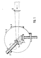
- FIG. 1 shows the apparatus used to carry out the method according to the invention.
- a pulsed excimer laser (Lambda Phys., EMG 201)
- the target 1 which is glued to a rotatable holder 2, is irradiated in a vacuum chamber 3 through a sapphire window 4 after focusing the beam with a cylindrical lens 5.
- the laser ablation achieved in this way leads to the formation of a plasma 6 which can be deposited on the substrate 8 heated by the heater 7.
- the distance between the target and the center of the substrate is about 3 cm.
- the exemplary embodiments specified below were carried out with a device of the type described, but at different temperatures, with different substrates and different target materials.
- the set oxygen partial pressure was 1 to 3 1 mbar in the exemplary embodiments and was set dynamically in the process.
- An adsorption pump was used as the pump and pure oxygen flows through the vacuum chamber.
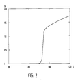
- FIG. 2 shows the resistance curve of a layer which was produced at a substrate surface temperature (T S ) of 780 ° C. (measured with a thermocouple).
- T S substrate surface temperature
- the curve shows a strong decrease in resistance to superconductivity in the region around 93 ° K. In this area, the resistance values at the beginning of the drop (100%) were measured at 90, 50, 10% of this value and when the value 0 was reached.
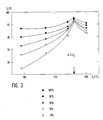
- These values are given in FIG. 3 in comparison to the corresponding values of the other layers produced at different substrate temperatures.
- the illustration in FIG. 3 shows that almost the same application points (100%) are achieved at other substrate temperatures, but the transitions become significantly wider. Studies on other substrates (ZrO2) show the same behavior.
- the critical current density of the films produced under optimal conditions (780 ° C, 1 mbar) on SrTiO3 was above 106 A / cm2 at 77K.
- the layers In contrast to the layers usually produced by laser ablation, the layers have very smooth surfaces with a surface roughness of ⁇ 0.2 ⁇ m and are therefore well suited for microstructuring in cryoelectric applications.
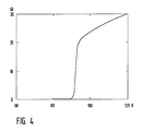
- FIG. 5 shows the resistance characteristic of a BiSrCaCuO layer, which is produced using a non-superconducting targets.
- the oxygen pressure was 1 mbar O2, the substrate temperature 780 ° C.
Landscapes
- Chemical & Material Sciences (AREA)
- Engineering & Computer Science (AREA)
- Chemical Kinetics & Catalysis (AREA)
- Materials Engineering (AREA)
- Mechanical Engineering (AREA)
- Metallurgy (AREA)
- Organic Chemistry (AREA)
- Physics & Mathematics (AREA)
- Inorganic Compounds Of Heavy Metals (AREA)
- Toxicology (AREA)
- Optics & Photonics (AREA)
- Manufacturing & Machinery (AREA)
- Thermal Sciences (AREA)
- Health & Medical Sciences (AREA)
- Superconductors And Manufacturing Methods Therefor (AREA)
- Superconductor Devices And Manufacturing Methods Thereof (AREA)
- Physical Vapour Deposition (AREA)
- Oxygen, Ozone, And Oxides In General (AREA)
Applications Claiming Priority (2)
| Application Number | Priority Date | Filing Date | Title |
|---|---|---|---|
| DE3822502A DE3822502C1 (fr) | 1988-07-03 | 1988-07-03 | |
| DE3822502 | 1988-07-03 |
Publications (2)
| Publication Number | Publication Date |
|---|---|
| EP0349910A2 true EP0349910A2 (fr) | 1990-01-10 |
| EP0349910A3 EP0349910A3 (fr) | 1990-09-26 |
Family
ID=6357868
Family Applications (1)
| Application Number | Title | Priority Date | Filing Date |
|---|---|---|---|
| EP19890111892 Withdrawn EP0349910A3 (fr) | 1988-07-03 | 1989-06-30 | Procédé pour la fabrication de couches minces supraconductrices à haute température contenant de l'oxyde |
Country Status (3)
| Country | Link |
|---|---|
| EP (1) | EP0349910A3 (fr) |
| JP (1) | JPH0288409A (fr) |
| DE (1) | DE3822502C1 (fr) |
Families Citing this family (5)
| Publication number | Priority date | Publication date | Assignee | Title |
|---|---|---|---|---|
| DE3914476C1 (fr) * | 1989-05-02 | 1990-06-21 | Forschungszentrum Juelich Gmbh, 5170 Juelich, De | |
| JPH04104903A (ja) * | 1990-08-21 | 1992-04-07 | Kokusai Chodendo Sangyo Gijutsu Kenkyu Center | 酸化物高温超電導薄膜の製造方法 |
| ATE137811T1 (de) * | 1992-03-13 | 1996-05-15 | Du Pont | Verfahren zur herstellung von dünnen ueberzügen aus anorganischen oxiden kontrollierter stöchiometrie |
| DE4210613C2 (de) * | 1992-03-31 | 1994-12-22 | Siemens Ag | Einrichtung zur Beschichtung eines Substrates mit einem metalloxidischen Hoch-T¶c¶-Supraleitermaterial |
| DE4321817C2 (de) * | 1993-07-01 | 1996-06-05 | Forschungszentrum Juelich Gmbh | Verfahren zur Herstellung eines Schichtsystems mit wenigstens einer Schicht aus einem metalloxidischen supraleitenden Material |
Family Cites Families (1)
| Publication number | Priority date | Publication date | Assignee | Title |
|---|---|---|---|---|
| DE3816192A1 (de) * | 1988-05-11 | 1989-11-23 | Siemens Ag | Verfahren zur herstellung einer schicht aus einem metalloxidischen supraleitermaterial mittels laser-verdampfens |
-
1988
- 1988-07-03 DE DE3822502A patent/DE3822502C1/de not_active Expired
-
1989
- 1989-06-30 EP EP19890111892 patent/EP0349910A3/fr not_active Withdrawn
- 1989-07-03 JP JP1171759A patent/JPH0288409A/ja active Pending
Also Published As
| Publication number | Publication date |
|---|---|
| EP0349910A3 (fr) | 1990-09-26 |
| JPH0288409A (ja) | 1990-03-28 |
| DE3822502C1 (fr) | 1989-08-24 |
Similar Documents
| Publication | Publication Date | Title |
|---|---|---|
| DE69007854T2 (de) | Verfahren und Apparatur zur Herstellung eines oxydsupraleitenden Drahtes. | |
| DE69416494T2 (de) | Vorrichtung um Schichten zu erzeugen und Verfahren um eine Schichtenstruktur mit dünnen Schichten aus supraleitendem Oxyd herzustellen | |
| DE3877116T2 (de) | Koerper mit supraleitendem oxid und dessen herstellungsverfahren. | |
| DE68926087T2 (de) | Methode zur Bildung eines Schwach-Kopplungs-Josephson-Übergangs und supraleitende Einrichtung, welche diesen Übergang benutzt | |
| DE3852979T2 (de) | Verfahren und Vorrichtung zur Herstellung supraleitender Dünnschichten. | |
| EP0341520B1 (fr) | Méthode de fabrication d'une couche mince d'oxyde métallique supraconducteur par évaporation au moyen d'un laser | |
| DE3854754T2 (de) | Supraleitende Schaltungen aus Keramik und Verfahren zu ihrer Herstellung. | |
| DE10212126A1 (de) | Supraleitender Magnesiumdiborid-Dünnfilm und Verfahren und Vorrichtung zu seiner Herstellung | |
| DE3933713C2 (fr) | ||
| EP0328757B1 (fr) | Procédé de fabrication de couches minces en supraconducteurs à Tc élevé de type oxyde | |
| DE112009002003B3 (de) | Verfahren zum Herstellen eines supraleitenden Oxid-Dünnfilms | |
| EP2644738A1 (fr) | Procédé d'injection par plasma pour la fabrication d'une membrane conductrice d'ions ainsi que la membrane en question | |
| DE69115957T2 (de) | Verfahren zum Herstellen hochtemperatursupraleitender Dünnschichten | |
| DE69116399T2 (de) | Verfahren zur Herstellung einer Schicht aus supraleitendem Oxyd | |
| DE69519703T2 (de) | Verfahren zum Herstellen einer hochkristallinen dünnen Oxidfilms und Beschichtigungsvorrichtung für dieses Verfahren | |
| DE3822502C1 (fr) | ||
| DE69218835T2 (de) | Laserablationprozess zum Herstellen supraleitender Dünnschichten aus oxydisch supraleitendem Verbindungsmaterial und Gerät zur Durchführung des Prozesses | |
| EP2368280A1 (fr) | Procédé de fabrication de substrats métalliques pour agencements stratifiés supraconducteurs à haute température (hts) | |
| DE19727343A1 (de) | Verfahren zur Erzeugung einer supraleitfähigen Schicht | |
| DE69205903T2 (de) | Verfahren und Apparatur zur Herstellung eines dünnen Oxidfilmes. | |
| DE69315736T2 (de) | Verfahren zur Herstellung von supraleitenden dünnen Schichten aus supraleitendem Oxidmaterial | |
| EP0361265A1 (fr) | Fabrication de couches minces d'un supraconducteur haute température par un procédé de dépôt en phase vapeur (PVD) activé par plasma | |
| DE69018539T2 (de) | Verfahren zur Herstellung von supraleitenden Dünnschichten. | |
| DE69404067T2 (de) | Verfahren zum Ablegen einer anderen Dünnschicht auf einer Oxyd-Dünnschicht mit perovskiter Kristallstruktur | |
| DE69115775T2 (de) | Prozess zur Abscheidung einer anderen Dünnschicht auf einen oxydischen Supraleiter |
Legal Events
| Date | Code | Title | Description |
|---|---|---|---|
| PUAI | Public reference made under article 153(3) epc to a published international application that has entered the european phase |
Free format text: ORIGINAL CODE: 0009012 |
|
| AK | Designated contracting states |
Kind code of ref document: A2 Designated state(s): CH FR GB IT LI NL |
|
| RAP3 | Party data changed (applicant data changed or rights of an application transferred) |
Owner name: FORSCHUNGSZENTRUM JUELICH GMBH |
|
| PUAL | Search report despatched |
Free format text: ORIGINAL CODE: 0009013 |
|
| AK | Designated contracting states |
Kind code of ref document: A3 Designated state(s): CH FR GB IT LI NL |
|
| 17P | Request for examination filed |
Effective date: 19901227 |
|
| 17Q | First examination report despatched |
Effective date: 19930319 |
|
| STAA | Information on the status of an ep patent application or granted ep patent |
Free format text: STATUS: THE APPLICATION HAS BEEN WITHDRAWN |
|
| 18W | Application withdrawn |
Withdrawal date: 19931211 |