EP0348843A2 - Lichtempfindliches Element für Elektrophotographie - Google Patents
Lichtempfindliches Element für Elektrophotographie Download PDFInfo
- Publication number
- EP0348843A2 EP0348843A2 EP89111472A EP89111472A EP0348843A2 EP 0348843 A2 EP0348843 A2 EP 0348843A2 EP 89111472 A EP89111472 A EP 89111472A EP 89111472 A EP89111472 A EP 89111472A EP 0348843 A2 EP0348843 A2 EP 0348843A2
- Authority
- EP
- European Patent Office
- Prior art keywords
- atomic
- photosensitive member
- gas
- film
- films
- Prior art date
- Legal status (The legal status is an assumption and is not a legal conclusion. Google has not performed a legal analysis and makes no representation as to the accuracy of the status listed.)
- Granted
Links
Images






Classifications
-
- G—PHYSICS
- G03—PHOTOGRAPHY; CINEMATOGRAPHY; ANALOGOUS TECHNIQUES USING WAVES OTHER THAN OPTICAL WAVES; ELECTROGRAPHY; HOLOGRAPHY
- G03G—ELECTROGRAPHY; ELECTROPHOTOGRAPHY; MAGNETOGRAPHY
- G03G5/00—Recording-members for original recording by exposure, e.g. to light, to heat or to electrons; Manufacture thereof; Selection of materials therefor
- G03G5/02—Charge-receiving layers
- G03G5/04—Photoconductive layers; Charge-generation layers or charge-transporting layers; Additives therefor; Binders therefor
- G03G5/08—Photoconductive layers; Charge-generation layers or charge-transporting layers; Additives therefor; Binders therefor characterised by the photoconductive material being inorganic
- G03G5/082—Photoconductive layers; Charge-generation layers or charge-transporting layers; Additives therefor; Binders therefor characterised by the photoconductive material being inorganic and not being incorporated in a bonding material, e.g. vacuum deposited
- G03G5/08214—Silicon-based
- G03G5/08278—Depositing methods
-
- G—PHYSICS
- G03—PHOTOGRAPHY; CINEMATOGRAPHY; ANALOGOUS TECHNIQUES USING WAVES OTHER THAN OPTICAL WAVES; ELECTROGRAPHY; HOLOGRAPHY
- G03G—ELECTROGRAPHY; ELECTROPHOTOGRAPHY; MAGNETOGRAPHY
- G03G5/00—Recording-members for original recording by exposure, e.g. to light, to heat or to electrons; Manufacture thereof; Selection of materials therefor
- G03G5/02—Charge-receiving layers
- G03G5/04—Photoconductive layers; Charge-generation layers or charge-transporting layers; Additives therefor; Binders therefor
- G03G5/08—Photoconductive layers; Charge-generation layers or charge-transporting layers; Additives therefor; Binders therefor characterised by the photoconductive material being inorganic
- G03G5/082—Photoconductive layers; Charge-generation layers or charge-transporting layers; Additives therefor; Binders therefor characterised by the photoconductive material being inorganic and not being incorporated in a bonding material, e.g. vacuum deposited
- G03G5/08214—Silicon-based
Definitions
- the invention relates to an electrophotographic photosensitive member used in electrophotographic imaging processes, and more particularly to a electrophotographic photoreceptor for xerographic systems.
- an amorphous silicon nitride containing H, amorphous silicon carbide containing H or amorphous silicon oxide containing H, each hereinafter called as a-SiN, a-SiC or a-SiO photoconductive film is expected to utilize for a photoconductive layer of an electrophotographic photoreceptor. Because, the photoreceptor composed of such photosensitive members shows (1) long life, (2) harmless to men and (3) high photosensitivity.
- a-SiN, a-SiC or a-SiO photoconductive film has been prepared by plasma CVD method or sputtering method, where H content in these films has been limited to be in the range of 10 - 40 atomic % (see USP 4,471,042).
- Each of the a-SiN, a-SiC and a-SiO photoconductive films can do, only by prescribing the specific amount of N, C or O in the film and by doping B, reach dark conductivity of about 10 ⁇ 13 ⁇ 1cm ⁇ 1 to be usable for photosensitive member.
- the a-SiC and a-SiO photoconductive films surely have an lower dark conductivity but simultaneously lower photosensitivity, so that practical use has been hindered in this regard.
- the a-SiN photoconductive film has been revealed through the inventor's experiments that in its repeat operation on next charging process after exprosure or photo-discharge, the surface potential lowers 20% or more of an initial value.
- the conventional type photoreceptor using a-SiN film as a photoconcuctive layer is quite poor in dark decay characteristics to thereby be not suitable for practical use.
- gap states such as dangling bond density of Si and the like increas due to the incorporation of N, so that carriers excited by exposure and photo-discharge will be trapped into the gapstates and then will be released from them by the electric field applied on a next charging process thereby removing the surface charges.
- the plasma CVD method or sputtering method has been adopted to prepare the conventional a-SiC, a-SiN and a-SiO photoconductive films, which inevitably caused to yield a polymeric powder of (SiH2) n which adsorbs on a film surface during deposition to thereby hinder a normal growth of film, and also needed a long time for the film formation due to low deposition rate thereof to thereby remain a drawback for cost saving.
- a photosensitive member for electrophotography which comprises a conductive substrate and a photoconductive layer in which the photoconductive layer is an amorphous silicon containing 40 - 50 atomic % of hydrogen and/or halogen and at least one chemical modifier selected from carbon, nitrogen and oxygen and fabricated by elctron cyclotron resonance method.
- the electrophotographic photosensitive members of the present invention show very low in dark conductivity and sufficient photosensitivity to be put into practical use, and also are superior in dark decay characteristics upon repeat operation.
- the manufacturing method of the present invention it can economically provide the photosensitive members because of high deposition rate and high productivity.
- the electrophotographic photosensitive member of the present invention comprises basically a conductive substrate and a photoconductive layer but may provide an intermediate layer therebetween and a surface protecting layer on a free surface of the photoconductive layer.
- the conductive substrate it may be used a conventional one available in the field, for example, a plate made from metals such as Al, Cr, Mo, Au, Ir, Nb, Ta, Pa, Pd and the like, or alloys from these metals. Also it may be a film or a sheet made of synthetic resins such as polyesters, polyethylenes, cellulose acetate, polypropylenes and the like, and a sheet made of glass, ceramics, those being given a conductive layer on its surface. Any shapes of the substrate may be used suitably for the purpose and is not limited to any particular configuration.
- the photoconductive layer of the invention contains at least one chemical modifier among C, N and O in amorphous silicaon.
- N content with respect to Si atom is usually 0.01 - 28 atomic %, preferably 0.2 - 28 atomic %.
- C content with respect to Si atom is usually 5 - 30 atomic %, preferably 10 - 30 atomic %.
- O content with respect to Si atom is usually 5 - 20 atomic %, preferably 10 - 20 atomic %.
- the content of hydrogen and/or halogen in the photoconductive layer is preferably at least 40 atomic %, and 60 atomic % at maximum.
- Such films with high content of hydrogen and/or halogen may be prepared by ECR method.
- the films with derived content may be obtained mainly by adjusting gas pressure during deposition under the condition of the high microwave power of 2.5 kW and without the substrate heating.
- the thickness of the photoconductive layer is usually 5 - 80 ⁇ m, preferably 10 - 50 ⁇ m.
- the photoconductive layer may contain impurities such as P or B. Such impurities may control the dark conductivity and the carrier transport property, so that they may be added when necessary.
- the intermediate layer serves to prevent the injection of carriers from the conductive substrate to the photoconductive layer, so that it may be provided when necessary.
- the intermediate layer is preferably formed by amorphous silicon and has usually a thickness of 2.0 - 20 ⁇ m.
- the surface protecting layer may be preferably provided for protecting the photosensitive member from physical or chemical damages such as corona discharge.
- the surface protecting layer may be amorphous silicon added with the same chemical modifier as that for the photoconductive layer and may preferably use a-SiC whose film thickness is usually 0.2 - 10 ⁇ m.
- ECR method is used for fabricating the photoconductive layer of the present invention.
- the ECR plasma CVD equipment is composed of a plasma formation chamber and a specimen chamber.
- the plasma formation chamber constructs a cavity resonator which is connected with the microwave source (a frequency of 2.45 GHz) through a rectangular waveguide, via microwave introducing window made from quartz.
- the microwave source a frequency of 2.45 GHz
- Around the plasma chamber are provided magnetic coils, and they give the electron cyclotron resonance condition and form the divergent magnetic field, which extract the plasma stream to a substrate.
- the specimen chamber includes a conductive substrate. When the substrate is a cylindrical type, it is supported by a support member to thereby be rotatable.
- a material gas of silicon compounds containing H or halogen such as SiH4, Si2H6, SiF4, SiCl4, SiHCl3, SiH2Cl2 and the like or mixture of these material gases.
- gas for supplying N effectively may include NH3 or N2 gas.
- the plasma formation chamber and specimen chamber are evacuated to vacuum so as to allow material gases to be introduced thereinto.
- gas pressure is usually set at 10 ⁇ 3 Torr - 10 ⁇ 4 Torr.
- a magnetic field and then supplied a microwave power so as to excite plasma, which is directed to the substrate through divergent magnetic field to cause a-SiN to be deposited. Since the support member is rotated, the film is uniformly deposited. The film uniformity can be improved by adjusting the position and the shape of plasma extracting orifice, which is arranged at the end opposite to the microwave introducing window.
- microwave power is 2.5 kW
- substrate is not heated.
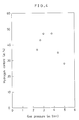
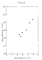
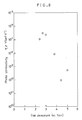
- Figs. 1, 2 and 3 show H content in the film, photo conductivity ( ⁇ ⁇ ⁇ ) at 565 nm, and dark conductivity ( ⁇ d ) dependent on gas pressure with respect to the obtained a-SiN films.
- the dark conductivity becomes less than 10 ⁇ 15 ⁇ 1cm ⁇ 1 without having boron doped and the photo conductivity is high (photosensitivity is high).
- the dark conductivity shows smaller.
- the dark conductivity is proportional to drift mobility ⁇ , so that in this region, it can be understood that lifetime ⁇ becomes larger.
- a silicon compound containing halogen is introduced as material gas, it requires that a total amount of H and halogen in the film is more than 40 atomic %. From additional experiments, it has been observed that when the amount of H and/or halogen in the film is set to be more than 60 atomic %, optical band gap of the film becomes too larger, so that this feature is not suitable for photoconductive layer for electrophotographic photosensitive member requiring photosensitivity with respect to visible light.
- a relevant content of H and/or halogen in the film is 40 - 60 atom %, preferably 43 - 55 atomic %.
- N content in the film is fixed in a range of 43 - 46 atomic % and a gaseous ratio of SiH4 and NH3 is changed to vary N content in the film.
- N content less than 0.01 atomic % there is no effect of decrease in the dark conductivity. It is considered that nitrogen acts as a donor and it causes the dark conductivity to be larger. Therefore, in this region, a-SiN films are not proper for photoconductive layer for electrophotographic photosensi tive member.
- N content more than 28 atomic % the photosensitivity to visible light is drastically lowered, which feature is also not suitable for photoconductive layer for electrophotographic photosensitive member.
- a usual value of N content with respect to Si atom is to be 0.01 - 28 atomic %, preferably 0.2 - 28 atomic %.
- material gases to be introduced are silicon compounds containing H or halogen such as SiH4, Si2H6, SiF4 SiCl4, SiHCl3 SiH2Cl2 and the like or mixture of these material gases.
- gases for C source may be such as CH4, C2H6 or C2H4, and gases for O source may be CO2, N2O or O2.
- Figs. 4 - 9 show H content in the film, photo conductivity ( ⁇ ⁇ ⁇ ) at 565 nm, dark conductivity ( ⁇ d ) dependent on gas pressure during deposition for a-SiC films and a-SiO films.
- the preparation conditions for these films are as follows.
- SiH4 + O2 145 sccm
- SiH4/(SiH4 + O2) 0.83
- microwave power 2.5 kW
- Figs. 10 and 11 show the relationships between photo conductivity ( ⁇ ⁇ ⁇ ), and dark conductivity ( ⁇ d ), and the film composition of a-SiC films or a-SiO films which were prepared in varying the flow rates of SiH4 and CH4, or SiH4 and O2, respectively.
- the other preparation conditions are the same as those of the films shown in Figs. 4 - 9 except for gas pressure fixed at 3.0 m Torr.
- the content of H and/or halogen is to be 40 - 60 atomic %.
- H content is more than 60 atomic %, H is bonded with Si in polymeric configuration of (SiH2) n to thereby deteriorate photo conductivity.
- the H and/or halogen content in these films is preferably 43 - 55 atomic %.
- the SiC films with C content more than 30 atomic % photo conductivity ( ⁇ ⁇ ⁇ ) shows less than 10 ⁇ 7 cm2/v, and less than 5 atomic %, dark conductivity ( ⁇ d ) is not drastically changed comparison with that of the film with no C content.
- the films with said characteristic is the object of the present invention.
- the C content in the a-SiC films is to be 5 - 30 atomic %, preferably 10 - 30 atomic %.
- the O content in the a-SiO films is to be 5 - 20 atomic %, preferably 10 - 20 atomic % on the same reason mentioned above for said C content.
- the photoconductive films according to the present invention are most suitably usable for a photosensitive device adapted to convert optical informations to electrical signals, such as those provided in electrophotography, image sensor or display in a coupled configuration with a liquid crystal.
- the invention is also applicable to such a device as solar battery, thin film transister.
- a cylindrical conductive substrate made of Al is mounted in the specimen chamber.
- SiH4 gas of 120 sccm and B2H6 gas of 20 sccm (diluted by H2 to 3000 ppm) are fed into the specimen chamber, so that an intermediate layer comprised of a-Si of 2.5 ⁇ m thickness is fabricated on the conductive substrate by ECR method under the condition of gas pressure of 3.0 m Torr and microwave power of 2.5 kW.
- the N content (N/Si) and the hydrogen content in the a-SiN photoconductive layer is 11 atomic % and 48 atomic %, respectively.
- the electrophotographic photoreceptor In the preparation process of the electrophotographic photoreceptor, there is no formation of polymeric powder of (SiH2) n , and deposition rate and gas usage efficiency have a considerable higher (6 - 10 times higher) value in comparison with those in the conventional art. Additionally, the obtained electrophotographic photo receptor showed a superiority in dark decay characteristics, particularly upon repeat operation. Furthermore, the electrophotographic photoreceptor was evaluated in a commercially available duplicator and provided a favourable image quality.
- N content (N/Si) was 9 - 12 atomic %.
- Table 1 Gas pressure (m Torr) 2.7 3.3 3.6 4.2 4.8 Dark decay characteristics o o ⁇ ⁇ ⁇ Image quality o o ⁇ ⁇ ⁇ ⁇
- An intermediate layer comprised of a-Si with 2.5 ⁇ m thickness was fabricated on the cylindrical conductive support member made of Al by ECR method under such conditions as microwave power of 2.5 kW, gas pressure of 2.7 m Torr and SiH4 gas of 120 sccm, B2H6 gas of 22 sccm (diluted by H2 to 3000 ppm), and NO gas of 12 sccm.
- a photoconductive layer comprised of a-SiC with 28 ⁇ m thickness was made on the intermediate layer by ECR method under such conditions as microwave power of 2.5 kW, gas pressure of 2.7 m Torr and SiH4 gas of 120 sccm, CH4 gas of 25 sccm and B2H6 gas of 40 sccm (diluted by H2 to 30 ppm).
- a surface layer comprised of a-SiC with 0.3 ⁇ m thickness was fabricated on the photoconductive layer under such conditions as microwave power of 1.5 kW, gas pressure of 0.8 m Torr and SiH4 gas of 10 sccm and CH4 gas of 18 sccm, whereby an electrophotographic photoreceptor could be obtained.
- the carbon content in the photoconductive layer was 20 atomic %, and the hydrogen content was 43 atomic %. Also, it was found that the deposition rate for the photoconductive layer was about 23 ⁇ m/hour which notably improved in comparison with the case of that (about 10 ⁇ m/hour) of the conventional plasma CVD method.
- the conductive support member was not heated and there observed no formation of polymeric powder of (SiH2) n . Measurement of the obtained electrophotographic photoreceptor for positive charge showed a favourable photosensitivity, less amount of residual potential, and is superior particularly in dark decay characteristics. Also, the electrophotographic photoreceptor was evaluated in a commercially available duplicator for positive charge and could provide a favourable image quality without having fogging.
- an electrophotographic photoreceptor was made. Measurement of the obtained electrophotographic photoreceptor showed that it has a favourable photosensitivity, less residual potential and is superior particularly in dark decay characteristics, as the same results in the Example 5 except for polarity. Furthermore, the electrophotographic photoreceptor was evaluated in a commercially available duplicator for negative charge and could provide a favourable image quality without having fogging.
Landscapes
- Chemical & Material Sciences (AREA)
- Inorganic Chemistry (AREA)
- Physics & Mathematics (AREA)
- General Physics & Mathematics (AREA)
- Photoreceptors In Electrophotography (AREA)
Applications Claiming Priority (6)
| Application Number | Priority Date | Filing Date | Title |
|---|---|---|---|
| JP161978/88 | 1988-06-28 | ||
| JP16197888A JPH028858A (ja) | 1988-06-28 | 1988-06-28 | 電子写真感光体 |
| JP161209/88 | 1988-06-29 | ||
| JP161210/88 | 1988-06-29 | ||
| JP16120988A JPH0210369A (ja) | 1988-06-29 | 1988-06-29 | 電子写真感光体 |
| JP16121088A JPH0210370A (ja) | 1988-06-29 | 1988-06-29 | 電子写真感光体 |
Publications (3)
| Publication Number | Publication Date |
|---|---|
| EP0348843A2 true EP0348843A2 (de) | 1990-01-03 |
| EP0348843A3 EP0348843A3 (en) | 1990-12-12 |
| EP0348843B1 EP0348843B1 (de) | 1996-02-28 |
Family
ID=27321822
Family Applications (1)
| Application Number | Title | Priority Date | Filing Date |
|---|---|---|---|
| EP89111472A Expired - Lifetime EP0348843B1 (de) | 1988-06-28 | 1989-06-23 | Lichtempfindliches Element für Elektrophotographie |
Country Status (3)
| Country | Link |
|---|---|
| US (1) | US5009977A (de) |
| EP (1) | EP0348843B1 (de) |
| DE (1) | DE68925760T2 (de) |
Cited By (1)
| Publication number | Priority date | Publication date | Assignee | Title |
|---|---|---|---|---|
| US5933831A (en) * | 1998-01-09 | 1999-08-03 | Lsi Logic Corporation | Viewing entity relationship diagrams using hyperlinks |
Families Citing this family (1)
| Publication number | Priority date | Publication date | Assignee | Title |
|---|---|---|---|---|
| US5239397A (en) * | 1989-10-12 | 1993-08-24 | Sharp Kabushiki | Liquid crystal light valve with amorphous silicon photoconductor of amorphous silicon and hydrogen or a halogen |
Family Cites Families (9)
| Publication number | Priority date | Publication date | Assignee | Title |
|---|---|---|---|---|
| US4265991A (en) * | 1977-12-22 | 1981-05-05 | Canon Kabushiki Kaisha | Electrophotographic photosensitive member and process for production thereof |
| US4471042A (en) * | 1978-05-04 | 1984-09-11 | Canon Kabushiki Kaisha | Image-forming member for electrophotography comprising hydrogenated amorphous matrix of silicon and/or germanium |
| JPS57119361A (en) * | 1981-01-16 | 1982-07-24 | Canon Inc | Image forming member for electrophotography |
| JPS59159167A (ja) * | 1983-03-01 | 1984-09-08 | Zenko Hirose | アモルフアスシリコン膜の形成方法 |
| US4705732A (en) * | 1984-04-27 | 1987-11-10 | Canon Kabushiki Kaisha | Member having substrate with projecting portions at surface and light receiving layer of amorphous silicon |
| JPH0740138B2 (ja) * | 1984-07-14 | 1995-05-01 | ミノルタ株式会社 | 電子写真感光体 |
| US4698288A (en) * | 1985-12-19 | 1987-10-06 | Xerox Corporation | Electrophotographic imaging members having a ground plane of hydrogenated amorphous silicon |
| US4760008A (en) * | 1986-01-24 | 1988-07-26 | Semiconductor Energy Laboratory Co., Ltd. | Electrophotographic photosensitive members and methods for manufacturing the same using microwave radiation in magnetic field |
| JPS6373259A (ja) * | 1986-09-16 | 1988-04-02 | Minolta Camera Co Ltd | 感光体 |
-
1989
- 1989-06-21 US US07/369,473 patent/US5009977A/en not_active Expired - Lifetime
- 1989-06-23 EP EP89111472A patent/EP0348843B1/de not_active Expired - Lifetime
- 1989-06-23 DE DE68925760T patent/DE68925760T2/de not_active Expired - Fee Related
Cited By (1)
| Publication number | Priority date | Publication date | Assignee | Title |
|---|---|---|---|---|
| US5933831A (en) * | 1998-01-09 | 1999-08-03 | Lsi Logic Corporation | Viewing entity relationship diagrams using hyperlinks |
Also Published As
| Publication number | Publication date |
|---|---|
| DE68925760T2 (de) | 1996-07-11 |
| EP0348843A3 (en) | 1990-12-12 |
| DE68925760D1 (de) | 1996-04-04 |
| US5009977A (en) | 1991-04-23 |
| EP0348843B1 (de) | 1996-02-28 |
Similar Documents
| Publication | Publication Date | Title |
|---|---|---|
| US4830946A (en) | CVD process for forming an image forming member for electrophotography | |
| US4495262A (en) | Photosensitive member for electrophotography comprises inorganic layers | |
| US5573884A (en) | Image-forming member for electrophotography | |
| US4670369A (en) | Image-forming member for electrophotography | |
| EP0926560A1 (de) | Elektrophotographisches lichtempfindliches Element | |
| US4468443A (en) | Process for producing photoconductive member from gaseous silicon compounds | |
| US5098736A (en) | Method for preparing electrophotographic photoreceptor | |
| US4859554A (en) | Multilayer photoreceptor | |
| EP0348843B1 (de) | Lichtempfindliches Element für Elektrophotographie | |
| JPH0782240B2 (ja) | 電子写真感光体 | |
| US4992348A (en) | Electrophotographic photosensitive member comprising amorphous silicon | |
| KR910006737B1 (ko) | 전자사진 광수용기 제조방법 | |
| JP2595575B2 (ja) | 電子写真感光体の製造方法 | |
| JP2720448B2 (ja) | 電子写真感光体の製造方法 | |
| EP0443521A1 (de) | Lichtempfindliches Element für Elektrophotographie | |
| US5057391A (en) | Photosensitive member for electrophotography and process for making using electron cyclotron resonance | |
| JP2668407B2 (ja) | 電子写真用像形成部材 | |
| EP0336700A2 (de) | Elektrophotographisches lichtempfindliches Element | |
| KR910003982B1 (ko) | 전자 사진 광수용체 | |
| JPH07117763B2 (ja) | 電子写真感光体の製造方法 | |
| JPH0647738B2 (ja) | プラズマcvd法による堆積膜形成方法 | |
| JPH07117764B2 (ja) | 電子写真感光体の製造方法 | |
| JPS58150963A (ja) | 光導電部材 | |
| JPH087448B2 (ja) | 電子写真感光体の製造方法 | |
| JPS61243458A (ja) | 感光体 |
Legal Events
| Date | Code | Title | Description |
|---|---|---|---|
| PUAI | Public reference made under article 153(3) epc to a published international application that has entered the european phase |
Free format text: ORIGINAL CODE: 0009012 |
|
| AK | Designated contracting states |
Kind code of ref document: A2 Designated state(s): DE FR GB |
|
| PUAL | Search report despatched |
Free format text: ORIGINAL CODE: 0009013 |
|
| AK | Designated contracting states |
Kind code of ref document: A3 Designated state(s): DE FR GB |
|
| 17P | Request for examination filed |
Effective date: 19901228 |
|
| 17Q | First examination report despatched |
Effective date: 19930621 |
|
| REG | Reference to a national code |
Ref country code: GR Ref legal event code: FG4A Free format text: 3013277 |
|
| REG | Reference to a national code |
Ref country code: GR Ref legal event code: MM2A Free format text: 3013277 |
|
| GRAA | (expected) grant |
Free format text: ORIGINAL CODE: 0009210 |
|
| AK | Designated contracting states |
Kind code of ref document: B1 Designated state(s): DE FR GB |
|
| REF | Corresponds to: |
Ref document number: 68925760 Country of ref document: DE Date of ref document: 19960404 |
|
| ET | Fr: translation filed | ||
| PLBE | No opposition filed within time limit |
Free format text: ORIGINAL CODE: 0009261 |
|
| STAA | Information on the status of an ep patent application or granted ep patent |
Free format text: STATUS: NO OPPOSITION FILED WITHIN TIME LIMIT |
|
| 26N | No opposition filed | ||
| REG | Reference to a national code |
Ref country code: GB Ref legal event code: IF02 |
|
| PGFP | Annual fee paid to national office [announced via postgrant information from national office to epo] |
Ref country code: FR Payment date: 20040608 Year of fee payment: 16 |
|
| PGFP | Annual fee paid to national office [announced via postgrant information from national office to epo] |
Ref country code: GB Payment date: 20040623 Year of fee payment: 16 |
|
| PGFP | Annual fee paid to national office [announced via postgrant information from national office to epo] |
Ref country code: DE Payment date: 20040701 Year of fee payment: 16 |
|
| PG25 | Lapsed in a contracting state [announced via postgrant information from national office to epo] |
Ref country code: GB Free format text: LAPSE BECAUSE OF NON-PAYMENT OF DUE FEES Effective date: 20050623 |
|
| PG25 | Lapsed in a contracting state [announced via postgrant information from national office to epo] |
Ref country code: DE Free format text: LAPSE BECAUSE OF NON-PAYMENT OF DUE FEES Effective date: 20060103 |
|
| PG25 | Lapsed in a contracting state [announced via postgrant information from national office to epo] |
Ref country code: FR Free format text: LAPSE BECAUSE OF NON-PAYMENT OF DUE FEES Effective date: 20060228 |
|
| GBPC | Gb: european patent ceased through non-payment of renewal fee |
Effective date: 20050623 |
|
| REG | Reference to a national code |
Ref country code: FR Ref legal event code: ST Effective date: 20060228 |