EP0348714A2 - Dispositif pour l'ajustage et la fixation d'une lentille sphérique et procédé pour l'utilisation du dispositif - Google Patents
Dispositif pour l'ajustage et la fixation d'une lentille sphérique et procédé pour l'utilisation du dispositif Download PDFInfo
- Publication number
- EP0348714A2 EP0348714A2 EP89110473A EP89110473A EP0348714A2 EP 0348714 A2 EP0348714 A2 EP 0348714A2 EP 89110473 A EP89110473 A EP 89110473A EP 89110473 A EP89110473 A EP 89110473A EP 0348714 A2 EP0348714 A2 EP 0348714A2
- Authority
- EP
- European Patent Office
- Prior art keywords
- carrier
- base
- legs
- optical waveguide
- photoelectric component
- Prior art date
- Legal status (The legal status is an assumption and is not a legal conclusion. Google has not performed a legal analysis and makes no representation as to the accuracy of the status listed.)
- Granted
Links
- 238000000034 method Methods 0.000 title claims description 8
- 230000003287 optical effect Effects 0.000 claims abstract description 19
- 230000005855 radiation Effects 0.000 claims abstract description 7
- 238000003892 spreading Methods 0.000 claims abstract description 5
- 238000003466 welding Methods 0.000 claims description 8
- 239000000463 material Substances 0.000 claims description 3
- 239000002184 metal Substances 0.000 claims description 2
- 229910001092 metal group alloy Inorganic materials 0.000 claims description 2
- 230000000149 penetrating effect Effects 0.000 claims 1
- 230000005540 biological transmission Effects 0.000 abstract description 10
- 239000013307 optical fiber Substances 0.000 abstract description 3
- 238000012634 optical imaging Methods 0.000 description 2
- 238000004026 adhesive bonding Methods 0.000 description 1
- 230000008878 coupling Effects 0.000 description 1
- 238000010168 coupling process Methods 0.000 description 1
- 238000005859 coupling reaction Methods 0.000 description 1
- 239000000835 fiber Substances 0.000 description 1
- 238000003384 imaging method Methods 0.000 description 1
- 238000003825 pressing Methods 0.000 description 1
- 238000005476 soldering Methods 0.000 description 1
- 239000000725 suspension Substances 0.000 description 1
Images
Classifications
-
- G—PHYSICS
- G02—OPTICS
- G02B—OPTICAL ELEMENTS, SYSTEMS OR APPARATUS
- G02B6/00—Light guides; Structural details of arrangements comprising light guides and other optical elements, e.g. couplings
- G02B6/24—Coupling light guides
- G02B6/42—Coupling light guides with opto-electronic elements
- G02B6/4201—Packages, e.g. shape, construction, internal or external details
- G02B6/4204—Packages, e.g. shape, construction, internal or external details the coupling comprising intermediate optical elements, e.g. lenses, holograms
-
- G—PHYSICS
- G02—OPTICS
- G02B—OPTICAL ELEMENTS, SYSTEMS OR APPARATUS
- G02B6/00—Light guides; Structural details of arrangements comprising light guides and other optical elements, e.g. couplings
- G02B6/24—Coupling light guides
- G02B6/42—Coupling light guides with opto-electronic elements
- G02B6/4201—Packages, e.g. shape, construction, internal or external details
- G02B6/4219—Mechanical fixtures for holding or positioning the elements relative to each other in the couplings; Alignment methods for the elements, e.g. measuring or observing methods especially used therefor
- G02B6/422—Active alignment, i.e. moving the elements in response to the detected degree of coupling or position of the elements
- G02B6/4226—Positioning means for moving the elements into alignment, e.g. alignment screws, deformation of the mount
-
- G—PHYSICS
- G02—OPTICS
- G02B—OPTICAL ELEMENTS, SYSTEMS OR APPARATUS
- G02B6/00—Light guides; Structural details of arrangements comprising light guides and other optical elements, e.g. couplings
- G02B6/24—Coupling light guides
- G02B6/42—Coupling light guides with opto-electronic elements
- G02B6/4201—Packages, e.g. shape, construction, internal or external details
- G02B6/4219—Mechanical fixtures for holding or positioning the elements relative to each other in the couplings; Alignment methods for the elements, e.g. measuring or observing methods especially used therefor
- G02B6/422—Active alignment, i.e. moving the elements in response to the detected degree of coupling or position of the elements
- G02B6/4225—Active alignment, i.e. moving the elements in response to the detected degree of coupling or position of the elements by a direct measurement of the degree of coupling, e.g. the amount of light power coupled to the fibre or the opto-electronic element
-
- G—PHYSICS
- G02—OPTICS
- G02B—OPTICAL ELEMENTS, SYSTEMS OR APPARATUS
- G02B6/00—Light guides; Structural details of arrangements comprising light guides and other optical elements, e.g. couplings
- G02B6/24—Coupling light guides
- G02B6/42—Coupling light guides with opto-electronic elements
- G02B6/4201—Packages, e.g. shape, construction, internal or external details
- G02B6/4219—Mechanical fixtures for holding or positioning the elements relative to each other in the couplings; Alignment methods for the elements, e.g. measuring or observing methods especially used therefor
- G02B6/4236—Fixing or mounting methods of the aligned elements
- G02B6/4237—Welding
Definitions
- the invention relates to a device according to the preamble of claim 1.
- a device is e.g. known from the company publications of the Hewlett Packard "Miniature Fiber Optic Logic Link” HFBR-0200 Series, December 1981, Fig. 1 and "Optical fiber components for data transmission” 5953-7700 12/81, p.2.
- a photoelectric transmitter e.g. a light emitting diode to feed outgoing light directly into an optical waveguide, or the light emerging from an optical waveguide directly into a receiving module, e.g. a photodiode
- a receiving module e.g. a photodiode
- ball lenses are usually used, which are arranged in the respective transmitting or receiving module between the photoelectric components and the optical waveguides. Their task is to bundle the light emanating from a photoelectric transmission component and to feed it into the optical waveguide or to focus the light emerging from the optical waveguide onto a photoelectric receiving element.
- the ball lenses are held mechanically in a suspension of the transmitter or receiver module.
- the spherical lens To achieve the desired imaging properties, it is necessary for the spherical lens to be aligned with high precision between the respective light-electrical component and the optical waveguide. This alignment must be more precise, the higher the demands on the transmission system. For high-quality transmission systems, it is necessary to adjust the ball lenses in the transmitter and receiver modules.
- the object of the present invention is to provide a device according to the preamble of claim 1, which allows a ball lens to be arranged in a simple and economical manner in the transmitting or receiving module so that the required optical imaging properties can be achieved.
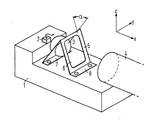
- the drawing schematically shows a base 1 arranged in the transmitting or receiving module of a photoelectric transmission path for receiving a photoelectric component 2 and a ball lens 3.
- the ball lens 3 is to be aligned and fixed between the photoelectric component 2 and an optical waveguide 4 so that the required optical imaging properties can be achieved.
- the ball lens 3 is fixed in a carrier 5, by means of which it can be aligned in all three coordinates X, Y and Z before or when it is fixed to the base 1.
- the carrier 5 consists of a band-shaped material which is angled transversely to its longitudinal axis and thereby forms two legs which collide in a V-shape.
- One leg of the carrier is provided with a recess for receiving the ball lens 3; the other has an opening 6 opposite this recess for the radiation emanating from or supplied to the photoelectric component 2.
- the ball lens 3 is mechanically fixed in the carrier 5 by suitable measures such as glazing, soldering, welding, gluing or pressing.
- the carrier has angled tabs 7 and 8 at the ends of the two legs, via which it is to be fastened to the base 1.
- the base 1 is flat in the area of the support 5 to be fastened to it.
- the attachment to the carrier is preferably carried out by welding the carrier tabs to the base.
- There is both Carrier as well as the base made of a weldable material, preferably a metal or a metal alloy.
- the process of adjusting and fixing a spherical lens proceeds as follows: First, the spherical lens 3 is to be aligned in the optical beam path by moving the carrier in the X and Y directions and adjusting the spreading angle ⁇ between the two legs of the carrier; this is determined by means of a suitable measuring apparatus. Then the leg of the carrier receiving the ball lens 3 is fixed to the base 1 by welding the leg to the base 1 via the angled tab 7; the welding points are indicated in the drawing by circles. The alignment or focusing of the radiation onto the optical waveguide or the photoelectric component is then checked and, if necessary, the height of the arrangement of the spherical lens is corrected by adjusting the spreading angle ⁇ between the two legs of the carrier 5.
- the other leg of the carrier 5 is welded to the base 1.
- the carrier is preferably applied to the base and the carrier is adjusted using a gripping tool for the sensitive positioning and adjustment of the carrier.
- the spherical lens is mechanically fixed in the beam path between the photoelectric component and the optical waveguide.
- the particular advantage of the device according to the invention can be seen in the fact that the highly precise adjustment and fixing of a spherical lens using a carrier designed as an inexpensive stamping / stamping part is possible with only low tolerance requirements.
- the spot welds of the carrier and the base require only a very short service life of the gripping tool during the fixing process.
- the thermal load on the surrounding structures during the welding process is low; A possible welding delay when welding the first carrier leg can be compensated for by readjusting the carrier.
- several devices, each with a spherical lens can be in the transmission Arrange or receive module of a photoelectric transmission path.
Landscapes
- Physics & Mathematics (AREA)
- General Physics & Mathematics (AREA)
- Optics & Photonics (AREA)
- Optical Couplings Of Light Guides (AREA)
Applications Claiming Priority (2)
| Application Number | Priority Date | Filing Date | Title |
|---|---|---|---|
| DE3822389 | 1988-07-01 | ||
| DE3822389 | 1988-07-01 |
Publications (3)
| Publication Number | Publication Date |
|---|---|
| EP0348714A2 true EP0348714A2 (fr) | 1990-01-03 |
| EP0348714A3 EP0348714A3 (en) | 1990-09-26 |
| EP0348714B1 EP0348714B1 (fr) | 1993-09-01 |
Family
ID=6357798
Family Applications (1)
| Application Number | Title | Priority Date | Filing Date |
|---|---|---|---|
| EP89110473A Expired - Lifetime EP0348714B1 (fr) | 1988-07-01 | 1989-06-09 | Dispositif pour l'ajustage et la fixation d'une lentille sphérique et procédé pour l'utilisation du dispositif |
Country Status (2)
| Country | Link |
|---|---|
| EP (1) | EP0348714B1 (fr) |
| DE (1) | DE58905432D1 (fr) |
Cited By (1)
| Publication number | Priority date | Publication date | Assignee | Title |
|---|---|---|---|---|
| EP0779526A3 (fr) * | 1995-12-13 | 1997-10-29 | Deutsche Telekom Ag | Connexion électrooptique et/ou optique et son procédé de fabrication |
Family Cites Families (4)
| Publication number | Priority date | Publication date | Assignee | Title |
|---|---|---|---|---|
| US3950075A (en) * | 1974-02-06 | 1976-04-13 | Corning Glass Works | Light source for optical waveguide bundle |
| NL7904283A (nl) * | 1979-05-31 | 1980-12-02 | Philips Nv | Koppelelement met een lichtbron en en lensvormig element. |
| DE3300902C2 (de) * | 1983-01-13 | 1985-01-10 | Hewlett-Packard GmbH, 7030 Böblingen | Zylindrisches Gehäuse für ein lichtemittierendes Halbleiterelement |
| JPS62276519A (ja) * | 1986-05-26 | 1987-12-01 | Hitachi Ltd | 光電子装置およびその製造方法ならびにレンズフレ−ム |
-
1989
- 1989-06-09 DE DE89110473T patent/DE58905432D1/de not_active Expired - Fee Related
- 1989-06-09 EP EP89110473A patent/EP0348714B1/fr not_active Expired - Lifetime
Cited By (1)
| Publication number | Priority date | Publication date | Assignee | Title |
|---|---|---|---|---|
| EP0779526A3 (fr) * | 1995-12-13 | 1997-10-29 | Deutsche Telekom Ag | Connexion électrooptique et/ou optique et son procédé de fabrication |
Also Published As
| Publication number | Publication date |
|---|---|
| EP0348714A3 (en) | 1990-09-26 |
| DE58905432D1 (de) | 1993-10-07 |
| EP0348714B1 (fr) | 1993-09-01 |
Similar Documents
| Publication | Publication Date | Title |
|---|---|---|
| DE68919327T2 (de) | Halbleiterlasermodul und methode zu seiner justierung. | |
| DE60025052T2 (de) | Vorrichtung zur Justierung einer Lichtquelle mit einer optischen Faser und ein diese enthaltendes optisches Modul | |
| EP0395854B1 (fr) | Arrangement pour coupler un guide d'onde avec un émetteur ou récepteur optique | |
| EP2073047B1 (fr) | Procédé de montage et d'ajustage d'un dispositif électro-optique et dispositif de mesure monté et ajusté selon un tel procédé | |
| DE69109317T2 (de) | Verfahren zur Herstellung eines optischen Kopplers. | |
| DE69522644T2 (de) | Vorrichtung zum Ankoppeln einer Lichtquelle an eine optische Faser | |
| DE19823934A1 (de) | Vorrichtung zum Koppeln einer Lichtquelle mit einer Lichtleitfaser | |
| DE19524475C1 (de) | Optische Zentriervorrichtung zum lagegenauen Bestücken eines Bauelements in Oberflächenmontagetechnik sowie deren Verwendung zur Montage von Laserdioden | |
| EP0992823B1 (fr) | Procédé de réglage d'un élément électrooptique | |
| DE4235549A1 (de) | Lichtquelleneinheit und herstellungsverfahren dafuer, einstellungsverfahren und einstellungsgeraet | |
| EP0990931A2 (fr) | Dispositif de réglage de composants optiques | |
| EP0590393A1 (fr) | Module à laser semiconducteur | |
| DE4344899A1 (de) | Dreh- und Ausrichtungsvorrichtung zum Zusammenbau eines Faseroptikverbinders mit geringeren Verbinderverlusten | |
| DE4009380A1 (de) | Lasermodul | |
| DE68914605T2 (de) | Element für optische Kopplung. | |
| EP0400161A1 (fr) | Dispositif de couplage optique d'un module convertisseur électrooptique avec une fibre optique au moyen de deux lentilles | |
| EP0348714B1 (fr) | Dispositif pour l'ajustage et la fixation d'une lentille sphérique et procédé pour l'utilisation du dispositif | |
| EP1913415B1 (fr) | Appareil de telemetrie et procede pour fixer une unite electro-optique a une unite support de conducteurs | |
| EP0388679A1 (fr) | Procédé pour aligner et fixer une lentille et système de couplage ainsi fabriqué | |
| DE3829350C2 (fr) | ||
| DE19751378B4 (de) | Verfahren und Vorrichtung zum Herstellen einer Abtasteinrichtung für optische Aufzeichnungsträger | |
| WO1998035252A1 (fr) | Module laser avec elements optiques de couplage et procede de reglage precis desdits elements optiques | |
| DE4133220C2 (de) | Fasern-Linsen-Anordnung zum optischen Koppeln | |
| DE2954697C2 (de) | Lasereinheit | |
| EP0918237A1 (fr) | Dispositif optique |
Legal Events
| Date | Code | Title | Description |
|---|---|---|---|
| PUAI | Public reference made under article 153(3) epc to a published international application that has entered the european phase |
Free format text: ORIGINAL CODE: 0009012 |
|
| AK | Designated contracting states |
Kind code of ref document: A2 Designated state(s): DE FR GB IT |
|
| PUAL | Search report despatched |
Free format text: ORIGINAL CODE: 0009013 |
|
| AK | Designated contracting states |
Kind code of ref document: A3 Designated state(s): DE FR GB IT |
|
| 17P | Request for examination filed |
Effective date: 19900828 |
|
| 17Q | First examination report despatched |
Effective date: 19920814 |
|
| GRAA | (expected) grant |
Free format text: ORIGINAL CODE: 0009210 |
|
| AK | Designated contracting states |
Kind code of ref document: B1 Designated state(s): DE FR GB IT |
|
| PG25 | Lapsed in a contracting state [announced via postgrant information from national office to epo] |
Ref country code: IT Free format text: LAPSE BECAUSE OF FAILURE TO SUBMIT A TRANSLATION OF THE DESCRIPTION OR TO PAY THE FEE WITHIN THE PRE;WARNING: LAPSES OF ITALIAN PATENTS WITH EFFECTIVE DATE BEFORE 2007 MAY HAVE OCCURRED AT ANY TIME BEFORE 2007. THE CORRECT EFFECTIVE DATE MAY BE DIFFERENT FROM THE ONE RECORDED.SCRIBED TIME-LIMIT Effective date: 19930901 Ref country code: GB Effective date: 19930901 Ref country code: FR Effective date: 19930901 |
|
| REF | Corresponds to: |
Ref document number: 58905432 Country of ref document: DE Date of ref document: 19931007 |
|
| EN | Fr: translation not filed | ||
| GBV | Gb: ep patent (uk) treated as always having been void in accordance with gb section 77(7)/1977 [no translation filed] |
Effective date: 19930901 |
|
| PLBE | No opposition filed within time limit |
Free format text: ORIGINAL CODE: 0009261 |
|
| STAA | Information on the status of an ep patent application or granted ep patent |
Free format text: STATUS: NO OPPOSITION FILED WITHIN TIME LIMIT |
|
| 26N | No opposition filed | ||
| PG25 | Lapsed in a contracting state [announced via postgrant information from national office to epo] |
Ref country code: DE Effective date: 19950301 |