EP0348640A2 - Halbleiteranordnung mit einer Schutzschicht - Google Patents
Halbleiteranordnung mit einer Schutzschicht Download PDFInfo
- Publication number
- EP0348640A2 EP0348640A2 EP89108386A EP89108386A EP0348640A2 EP 0348640 A2 EP0348640 A2 EP 0348640A2 EP 89108386 A EP89108386 A EP 89108386A EP 89108386 A EP89108386 A EP 89108386A EP 0348640 A2 EP0348640 A2 EP 0348640A2
- Authority
- EP
- European Patent Office
- Prior art keywords
- film
- protective film
- semiconductor device
- amorphous
- plasma
- Prior art date
- Legal status (The legal status is an assumption and is not a legal conclusion. Google has not performed a legal analysis and makes no representation as to the accuracy of the status listed.)
- Withdrawn
Links
Images


Classifications
-
- H10P95/00—
-
- H10W74/481—
Definitions
- the present invention relates to a semiconductor device in which a surface protective film or a protective interlayer is formed.
- a plasma SiN or SiO film As a passivation film serving as a surface protective film or a protective interlayer of a semiconductor device, a plasma SiN or SiO film is conventionally known.
- Fig. 1 is a sectional view showing an element structure of a conventional diode of a high breakdown voltage which is an example of a semiconductor device including a surface protective film.
- a p-type region 32 is selectively formed in a surface region of an n-type silicon substrate 31 by diffusion or the like.
- An SiO2 film 33 serving as a field passivation film is formed on the surface of the substrate 31, and an opening 34 is formed in a part of the SiO2 film 33 to expose the surface of the p-type region 32.
- An aluminum electrode 35 is formed in the opening 34.
- a passivation film 36 of, e.g., a plasma SiN or SiO film having a thickness of about 1 ⁇ m is deposited on the electrode 35.
- an insulating film such as a plasma SiN or SiO film is normally used as a passivation film.
- Insufficient potential shielding adversely affects not only the substrate but also an element surface.
- the passivation film 36 has no capability of shielding the potential. Therefore, when a bias voltage is applied to the electrode 35, a floating potential is generated on the surface of the passivation film 36 on the electrode. When this floating potential is generated, a potential difference is generated between the passivation film 36 and another electrode (not shown). Due to this potential difference, various impurity ions contained in the element, such as Na+, Ka+, Cl ⁇ , and OH ⁇ are moved. As the ions are moved, electrons are also moved in the substrate and concentrated at the interface near a p-n junction. Therefore, deterioration of element characteristics such as a decrease in breakdown voltage of the p-n junction occurs.
- the thickness of the passivation film 36 is increased, or the distance between the electrodes is increased.
- a crack tends to occur in the passivation film, thus degrading the reliability of the element.
- the element area is undesirably increased.
- an insulating film having an insufficient potential shielding effect is used as a surface protective film. Therefore, in order to improve the element characteristics, deterioration of the element reliability and an increase in element area may undesirably occur.
- a semiconductor device comprises a semiconductor substrate on which an elements are formed, and a surface protective film consisting of an amorphous semiconductor film formed on a semiconductor device.
- a semiconductor device comprises a semiconductor substrate on which elements are formed, a multi-wiring layer formed on the surface of the substrate, and an interlayer consisting of an amorphous semiconductor film formed between the wiring layers.
- amorphous semiconductor film used as the surface protective film on the semiconductor device or the interlayer between the wiring layers electric charge having an amount to cancel an external electric field is generated in the amorphous semiconductor film. For this reason, even if the thickness of the amorphous semiconductor film is not much increased, relaxation of the electric field on the substrate surface can be achieved.
- Fig. 3 is a sectional view showing an element structure when a semiconductor device including a surface protective film according to the present invention is applied to a diode having a high breakdown voltage.
- a p-type region 12 is selectively formed in a surface region of an n-type silicon substrate 11 by diffusion or the like.
- An SiO2 film 13 serving as a field passivation film is formed on the surface of the substrate 11, and an opening 14 is formed in a part of the SiO2 film 13 to expose the surface of the p-type region 12.
- An electrode 15 of, e.g., aluminum is formed in the opening 14.
- a surface protective film 16 consisting of an amorphous semiconductor film is formed on the electrode 15.
- a plasma SiC film having a thickness of about 1 ⁇ m formed by plasma CVD (plasma chemical vapor deposition) is used as the above-mentioned surface protective film 16.
- the plasma SiC film is formed as follows. An SiH4 (silane) gas and C3H8 (propan) gas are supplied in a vacuum container having a vacuum of 0.7 Torr at a flow rate of, e.g., 200 cc/min each, and the plasma SiC film is deposited at 250°c in a high-frequency discharge state of a current of 200 mA.
- the potential in the surface protective film 16 is quadratically decreased. Even if the thickness of the surface protective film 16 is not much increased, the potential in the surface protective film 16 is substantially "0" at the boundary between the surface protective film 16 and the silicon substrate 11. More specifically, the potential of the boundary between the surface protective film 16 and the silicon substrate 11 is "0", and even if the external electric field is applied, the potential does not adversely affect the substrate surface. In addition, since the surface protective film 16 has capability of shielding the potential, a potential difference between the electrodes does not tend to occur, as in the conventional case. Movement of various ions contained in the elements can be prevented, and deterioration of element characteristics such as an increase in breakdown voltage in a p-n junction is relaxed. Since the distance between the electrodes need not be increased, an increase in element area can be prevented.
- Figs. 5 and 6 are graphs showing a temperature change in resistivity ( ⁇ m) of the surface protective film 16 used in the semiconductor device of the above-mentioned embodiment.
- Fig. 5 shows characteristics in a low-temperature region
- Fig. 6 shows characteristics in a high-temperature region.
- the surface protective film 16 has electric conduction characteristics inherent in an amorphous semiconductor film.
- the value of the resistivity is 1011 ⁇ m or more, and the surface protective film 16 has a sufficient insulation property.
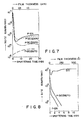
- Fig. 7 is a graph showing a diffused Na profile of the surface protective film 16 used in the semiconductor device of the above-mentioned embodiment, and that of a plasma SiN film used in the conventional semiconductor device.
- the formed films are removed by sputtering, and the numbers of Na and Si atoms obtained within unit time (1 sec) are counted.
- a ratio of the number of Na atoms to that of Si atoms, i.e., an Na/Si ratio (counts/sec) is calculated, so that the amount of Na contained in the original film is measured, thus determining the diffused Na profile.
- an Na/Si ratio counts/sec
- P-SiN represents a plasma SiN film used in the conventional semiconductor device
- P-SiC represents a plasma SiC film used in the semiconductor device according to the above-mentioned embodiment.
- Each value in parentheses represents a temperature when the corresponding film is deposited.
- the amount of Na is smallest, and a sufficient anti-Na property can be obtained.
- the anti-Na property is degraded about 100 times the amorphous plasma SiN film used in the semiconductor device of the above embodiment.
- Fig. 8 is a graph showing diffused deutrium profile of the surface protective film 16 used in the semiconductor device of the above-mentioned embodiment, and that of the plasma SiN and SiO films used in the conventional semiconductor device.
- the formed films are removed by sputtering, and the numbers of D (deutrium) and Si atoms obtained within unit time (1 sec) are counted.
- the ratio of the number of D atoms to that of Si atoms, i.e., a D/Si ratio (counts/sec) is calculated, so that the amount of deutrium contained in the original film is measured, thus determining the diffused deutrium profile.
- a D/Si ratio counts/sec
- P-SiN represents a plasma SiN film used in the conventional semiconductor device
- P-SiC represents a plasma SiC film used in the semiconductor device according to the above-mentioned embodiment.
- Each value in parentheses represents a temperature when the corresponding film is deposited.
- the plasma SiC film deposited at 380°C has substantially the diffused deutrium profile as that of the plasma SiN film used in the conventional semiconductor device.
- the plasma SiC film has a sufficient diffused Na profile and sufficient diffused deutrium profile. Therefore, the plasma SiC film can serve as a final surface protective film.
- the deposition rate of the plasma SiC film is higher than that of the plasma SiN film by about 25%, and the etching rate of the plasma SiC film is also higher than that of the plasma SiN film by about 20%. Therefore, the manufacturing time of the semiconductor device of the present invention can be effectively reduced, as compared with the conventional semiconductor device.
- Fig. 9 is a sectional view showing a semiconductor device according to another embodiment of the present invention.
- the semiconductor device according to the present invention is applied to a diode having a high breakdown voltage.
- a first protective film 17 consisting of an amorphous Si film which exhibits neither diffused Na profile nor diffused deutrium profile, or an amorphous semiconductor film such as a plasma SiO film having a low oxygen concentration, and which has no passivation capability
- a second protective film 18 which consists of an insulating film such as a plasma SiN or SiO film, and which has a passivation capability, are stacked on an electrode 15 of, e.g., aluminum.
- the amorphous Si film is formed as follows.
- An SiH4 gas is supplied in a vacuum container having a vacuum of 1.0 Torr at a flow rate of, e.g., 200 cc/min, and the amorphous Si film is deposited at 380°C in a state wherein a high-frequency current of 200 mA flows between the plasma electrodes.
- the plasma SiO film having a low oxygen concentration is formed as follows.
- An SiH4 gas and an N2O gas are supplied in a vacuum container having a vacuum of 1.0 Torr at a flow rate of, e.g., 200 cc/min, and the plasma SiO film is deposited at 380°C in a state wherein a high-frequency current of 200 mA flows.
- a sufficient potential shielding effect can be obtained by forming the first protective film 17 of the amorphous semiconductor film, and a passivation effect such as diffused Na profile and diffused deutrium profile can be obtained by forming the second protective film 18 of the insulating film.
- Fig. 10 shows a semiconductor device including a surface protective film according to still another embodiment of the present invention, and is a sectional view showing an element structure when the semiconductor device is applied to a diode having a high breakdown voltage and a multi-wiring structure.
- a p-type region 12 is selectively formed in a surface region of an n-type silicon substrate 11 by diffusion or the like.
- An SiO2 film 13 serving as a field passivation film is formed on the surface of the substrate 11, and an opening 14 is formed in a part of the SiO2 film 13 to expose the surface of the p-type region 12.
- An electrode 15 of, e.g., aluminum is formed in the opening 14.
- a protective film 19 consisting of an amorphous semiconductor film, e.g., a plasma SiC film is formed on the electrode 15.
- a protective film 20 of an insulating film such as a plasma SiN or SiO film is formed on the protective film 19.
- An opening 21 is formed in a part of a stacked film of the protective films 19 and 20 to expose the surface of the electrode 15.
- An electrode 22 of, e.g., aluminum is formed in the opening 21.
- the protective film 19 consisting of the amorphous semiconductor film is used as an interlayer between the wiring layers of the semiconductor device including a multiwiring layer. Therefore, since the amorphous film is sandwiched between the electrodes 15 and 22 respectively connected to the protective films 19 and 20, the electric field can be sufficiently relaxed, thus improving reliability.
- Fig. 11 is a graph showing leak current characteristics when a reverse bias voltage is applied to the p-n junction in the semiconductor device including a surface protective film according to the present invention shown in Fig. 3, and those when a reverse bias voltage is applied on the p-n junction in the conventional semiconductor device shown in Fig. 1.
- a characteristic curve I in Fig. 11 represents the characteristics of the semiconductor device according to the present invention shown in Fig. 3, and a characteristic curve II represents the characteristics of the conventional semiconductor device shown in Fig. 1.
- the characteristic curve II represents that ions adsorbed in the element surfaces are adversely affected by the electric field of the surface and approach the electrode, so that so-called "walk-out" occur.
Landscapes
- Formation Of Insulating Films (AREA)
- Internal Circuitry In Semiconductor Integrated Circuit Devices (AREA)
Applications Claiming Priority (2)
| Application Number | Priority Date | Filing Date | Title |
|---|---|---|---|
| JP113246/88 | 1988-05-10 | ||
| JP63113246A JPH01283838A (ja) | 1988-05-10 | 1988-05-10 | 半導体装置 |
Publications (2)
| Publication Number | Publication Date |
|---|---|
| EP0348640A2 true EP0348640A2 (de) | 1990-01-03 |
| EP0348640A3 EP0348640A3 (de) | 1990-06-13 |
Family
ID=14607278
Family Applications (1)
| Application Number | Title | Priority Date | Filing Date |
|---|---|---|---|
| EP89108386A Withdrawn EP0348640A3 (de) | 1988-05-10 | 1989-05-10 | Halbleiteranordnung mit einer Schutzschicht |
Country Status (3)
| Country | Link |
|---|---|
| EP (1) | EP0348640A3 (de) |
| JP (1) | JPH01283838A (de) |
| KR (1) | KR890017765A (de) |
Cited By (4)
| Publication number | Priority date | Publication date | Assignee | Title |
|---|---|---|---|---|
| EP0430345A1 (de) * | 1989-11-24 | 1991-06-05 | Philips Electronics Uk Limited | Dioden- und Anzeigevorrichtungen mit aktiver Matrixadressierung unter Verwendung einer solchen Diodenvorrichtung |
| EP0608335A4 (de) * | 1991-10-11 | 1994-11-17 | Vlsi Technology Inc | Struktur zur unterdrückung einer durch eine aufladung im dielektrikum verursachte feldumkehrung. |
| US5523604A (en) * | 1994-05-13 | 1996-06-04 | International Rectifier Corporation | Amorphous silicon layer for top surface of semiconductor device |
| DE19732217A1 (de) * | 1997-07-26 | 1999-02-11 | Zsw | Mehrfunktions-Verkapselungsschichtstruktur für photovoltaische Halbleiterbauelemente und Verfahren zu ihrer Herstellung |
Family Cites Families (8)
| Publication number | Priority date | Publication date | Assignee | Title |
|---|---|---|---|---|
| JPS51128268A (en) * | 1975-04-30 | 1976-11-09 | Sony Corp | Semiconductor unit |
| GB1566072A (en) * | 1977-03-28 | 1980-04-30 | Tokyo Shibaura Electric Co | Semiconductor device |
| US4134125A (en) * | 1977-07-20 | 1979-01-09 | Bell Telephone Laboratories, Incorporated | Passivation of metallized semiconductor substrates |
| US4273805A (en) * | 1978-06-19 | 1981-06-16 | Rca Corporation | Passivating composite for a semiconductor device comprising a silicon nitride (Si1 3N4) layer and phosphosilicate glass (PSG) layer |
| JPS59119733A (ja) * | 1982-12-24 | 1984-07-11 | Toshiba Corp | 半導体装置 |
| JPS6084824A (ja) * | 1983-10-17 | 1985-05-14 | Hitachi Ltd | 半導体装置の製造方法 |
| JPS60189226A (ja) * | 1984-03-08 | 1985-09-26 | Sharp Corp | コ−テイング膜 |
| JPS6379972A (ja) * | 1987-09-12 | 1988-04-09 | Semiconductor Energy Lab Co Ltd | 炭素被膜 |
-
1988
- 1988-05-10 JP JP63113246A patent/JPH01283838A/ja active Pending
-
1989
- 1989-05-09 KR KR1019890006173A patent/KR890017765A/ko not_active Abandoned
- 1989-05-10 EP EP89108386A patent/EP0348640A3/de not_active Withdrawn
Cited By (6)
| Publication number | Priority date | Publication date | Assignee | Title |
|---|---|---|---|---|
| EP0430345A1 (de) * | 1989-11-24 | 1991-06-05 | Philips Electronics Uk Limited | Dioden- und Anzeigevorrichtungen mit aktiver Matrixadressierung unter Verwendung einer solchen Diodenvorrichtung |
| EP0608335A4 (de) * | 1991-10-11 | 1994-11-17 | Vlsi Technology Inc | Struktur zur unterdrückung einer durch eine aufladung im dielektrikum verursachte feldumkehrung. |
| US5523604A (en) * | 1994-05-13 | 1996-06-04 | International Rectifier Corporation | Amorphous silicon layer for top surface of semiconductor device |
| US5654206A (en) * | 1994-05-13 | 1997-08-05 | International Rectifier Corporation | Amorphous silicon layer for top surface of semiconductor device |
| DE19732217A1 (de) * | 1997-07-26 | 1999-02-11 | Zsw | Mehrfunktions-Verkapselungsschichtstruktur für photovoltaische Halbleiterbauelemente und Verfahren zu ihrer Herstellung |
| DE19732217C2 (de) * | 1997-07-26 | 2002-12-12 | Zsw | Mehrfunktions-Verkapselungsschichtstruktur für photovoltaische Halbleiterbauelemente und Verfahren zu ihrer Herstellung |
Also Published As
| Publication number | Publication date |
|---|---|
| JPH01283838A (ja) | 1989-11-15 |
| KR890017765A (ko) | 1989-12-18 |
| EP0348640A3 (de) | 1990-06-13 |
Similar Documents
| Publication | Publication Date | Title |
|---|---|---|
| US4972250A (en) | Protective coating useful as passivation layer for semiconductor devices | |
| US5107323A (en) | Protective layer for high voltage devices | |
| US7042059B2 (en) | Optical semiconductor device and method for manufacturing optical semiconductor device | |
| US6670705B1 (en) | Protective layer for a semiconductor device | |
| CA1044377A (en) | Metal insulator semiconductor field effect device | |
| US8169052B2 (en) | Semiconductor device | |
| USH665H (en) | Resistive field shields for high voltage devices | |
| US3701931A (en) | Gold tantalum-nitrogen high conductivity metallurgy | |
| JP4242648B2 (ja) | 金属イオン拡散バリア層 | |
| JP3193632B2 (ja) | 酸化物のエッチング方法 | |
| EP0217326A2 (de) | Halbleiteranordnung mit einer hohen Durchbruchspannung | |
| US4121240A (en) | Semiconductor device having a discharge-formed insulating film | |
| EP0348640A2 (de) | Halbleiteranordnung mit einer Schutzschicht | |
| US3450581A (en) | Process of coating a semiconductor with a mask and diffusing an impurity therein | |
| US4161744A (en) | Passivated semiconductor device and method of making same | |
| GB1566072A (en) | Semiconductor device | |
| WO1990007796A1 (en) | Insulator films on diamond | |
| US5029324A (en) | Semiconductor device having a semiconductive protection layer | |
| US4224636A (en) | Semiconductor device with thermally compensating SiO2 -silicate glass-SiC passivation layer | |
| US3436612A (en) | Semi-conductor device having dielectric and metal protectors | |
| US20160358874A1 (en) | Semiconductor device | |
| US4380115A (en) | Method of making a semiconductor device with a seal | |
| US4960436A (en) | Radiation or light detecting semiconductor element containing heavily doped p-type stopper region | |
| JPH03289156A (ja) | 半導体装置およびその製造方法 | |
| Auret et al. | Characterization of defects introduced during dc magnetron sputter deposition of Ti–W on n‐Si |
Legal Events
| Date | Code | Title | Description |
|---|---|---|---|
| PUAI | Public reference made under article 153(3) epc to a published international application that has entered the european phase |
Free format text: ORIGINAL CODE: 0009012 |
|
| 17P | Request for examination filed |
Effective date: 19890510 |
|
| AK | Designated contracting states |
Kind code of ref document: A2 Designated state(s): DE FR GB |
|
| PUAL | Search report despatched |
Free format text: ORIGINAL CODE: 0009013 |
|
| AK | Designated contracting states |
Kind code of ref document: A3 Designated state(s): DE FR GB |
|
| STAA | Information on the status of an ep patent application or granted ep patent |
Free format text: STATUS: THE APPLICATION IS DEEMED TO BE WITHDRAWN |
|
| 18D | Application deemed to be withdrawn |
Effective date: 19921201 |