EP0348079A2 - Symmetrischer integrierter Verstärker mit gesteuerter Offset-Gleichspannung - Google Patents
Symmetrischer integrierter Verstärker mit gesteuerter Offset-Gleichspannung Download PDFInfo
- Publication number
- EP0348079A2 EP0348079A2 EP89305852A EP89305852A EP0348079A2 EP 0348079 A2 EP0348079 A2 EP 0348079A2 EP 89305852 A EP89305852 A EP 89305852A EP 89305852 A EP89305852 A EP 89305852A EP 0348079 A2 EP0348079 A2 EP 0348079A2
- Authority
- EP
- European Patent Office
- Prior art keywords
- fet
- amplifier
- drain
- gate
- source
- Prior art date
- Legal status (The legal status is an assumption and is not a legal conclusion. Google has not performed a legal analysis and makes no representation as to the accuracy of the status listed.)
- Granted
Links
Images


Classifications
-
- H—ELECTRICITY
- H03—ELECTRONIC CIRCUITRY
- H03F—AMPLIFIERS
- H03F3/00—Amplifiers with only discharge tubes or only semiconductor devices as amplifying elements
- H03F3/04—Amplifiers with only discharge tubes or only semiconductor devices as amplifying elements with semiconductor devices only
- H03F3/16—Amplifiers with only discharge tubes or only semiconductor devices as amplifying elements with semiconductor devices only with field-effect devices
-
- H—ELECTRICITY
- H03—ELECTRONIC CIRCUITRY
- H03F—AMPLIFIERS
- H03F1/00—Details of amplifiers with only discharge tubes, only semiconductor devices or only unspecified devices as amplifying elements
- H03F1/30—Modifications of amplifiers to reduce influence of variations of temperature or supply voltage or other physical parameters
- H03F1/306—Modifications of amplifiers to reduce influence of variations of temperature or supply voltage or other physical parameters in junction-FET amplifiers
-
- H—ELECTRICITY
- H03—ELECTRONIC CIRCUITRY
- H03F—AMPLIFIERS
- H03F1/00—Details of amplifiers with only discharge tubes, only semiconductor devices or only unspecified devices as amplifying elements
- H03F1/30—Modifications of amplifiers to reduce influence of variations of temperature or supply voltage or other physical parameters
- H03F1/307—Modifications of amplifiers to reduce influence of variations of temperature or supply voltage or other physical parameters in push-pull amplifiers
- H03F1/309—Modifications of amplifiers to reduce influence of variations of temperature or supply voltage or other physical parameters in push-pull amplifiers using junction-FET
Definitions
- the present invention relates to a symmetric integrated amplifier with controlled DC offset voltage and, more particularly, to such an amplifier which is insensitive to variations in either the power supply voltages or transistor threshold voltage.
- OEICs opto-electronic integrated circuits
- a clear advantage of such OEICs is their small size relative to the bulk devices in use today.
- a problem being currently addressed in the art is providing a substrate material, and corresponding fabrication techniques, which is compatible with both the optical and electronic components.
- Most electronic integrated circuits is use today are formed on a silicon substrate, where silicon is not a preferred substrate material for lightwave devices, including lasers, LEDs, or photodiodes.
- OEICs are formed on indium phosphide (InP) substrates, with lattice-matched GaInAsP material grown on the InP substrate for lightwave device formation.
- InP indium phosphide
- FET field effect transistor
- JFETs included in separate photoreceivers may exhibit vastly different threshold voltages, due to the relatively complex InP-based JFET fabrication process.
- the latter problem creates a significant impediment to the formation of multi-stage amplifiers, since the output voltages from the cascaded stages will be unknown and thus uncontrollable.
- a conventional prior art FET amplifier is discussed by D. P. Hornbuckle et al. in a paper entitled "Monolithic GaAs Direct-Coupled Amplifiers" appearing in IEEE Transactions on Electron Devices, Vol. ED-28, No. 2, February 1981 at pp. 175-182.
- the Hornbuckle et al. amplifier includes a first FET to which an input voltage signal V IN is applied.
- An active load consisting of a gate-source coupled second FET is connected between the drain of the first FET and a first power supply, denoted VDD.
- An active load is considered to be superior to a common resistor load between drain and power supply in that the active load provides for improved large-signal performance.
- this arrangement will amplify and invert the applied voltage V IN .
- the portion of the circuit described to this point could be cascaded, with appropriate capacitive coupling, to form a multistage amplifier, where the gain of the multistage arrangement would be a multiplicative increase over the gain of this single stage.
- the bandwidth of such an arrangement would be significantly reduced for two reasons: (1) the capacitor between stages will limit the low frequency response, and (2) the high frequency response will be limited by the high output impedance of the inverter circuit.
- capacitive coupling is required to eliminate the DC offset voltage of the amplified signal introduced by the FETs.
- This capacitive loading is thus significantly reduced in the Hornbuckle et al. amplifier by applying the inverted V IN appearing at the drain of the first FET to the gate of a third FET, referred to as a buffer FET, the drain of the buffer FET being directly coupled to VDD.
- a buffer FET Connected between the source of buffer FET and the output of the amplifier is a pair of level shifting diodes, where each diode will contribute an approximate voltage drop of 1V to the inverted V IN appearing at the FET.
- the diodes may be formed as FETs, with their respective sources and drains connected.
- a DC voltage offset may arise when the individual FET characteristics, most notably the threshold voltage, change for a fixed power supply.
- This DC offset voltage can be removed by either separately adjusting the power supply voltages (VSS,VDD), or by adjusting the bias to the gate of a current source FET which will, in turn, change the bias current for the level shifting diodes.
- VSS,VDD power supply voltages
- a current source FET which will, in turn, change the bias current for the level shifting diodes.
- the present invention relates to a symmetric integrated amplifier with controlled voltage offset and, more particularly, to such an amplifier which is insensitive to variations in either the power supply voltages or transistor threshold voltages.
- a symmetric amplifier arrangement which provides (in the quiescent state) an identical voltage drop between each power supply (VDD,VSS) and the amplifier output.
- This voltage drop is provided by a series of transistors and diodes inserted between each power supply and the output node.
- the number of diodes is a matter of design choice, where the diodes may be formed by gate-source connection of JFET devices.
- the threshold voltage of InP-based JFET devices may vary by several volts, as a result of variations in the fabrication process.
- the DC offset voltage of conventional JFET amplifiers formed in InP may also vary. This variation in DC offset voltage makes the formation of any type of multi-stage amplifier impossible.
- An advantage of the symmetric arrangement of the present invention is that virtually no DC offset voltage is present if the portion of the circuit connected between VDD and the output is identical to the portion of the circuit between VSS and this same output node.
- a multi-stage amplifier may be formed when utilizing the symmetric arrangement of the present invention merely by directly coupling single stage amplifiers together in series. Direct coupling, as will be discussed below, is preferred over capacitive coupling in that it does not affect the bandwidth of the multistage amplifier.
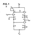
- Symmetric amplifier 30 like the Hornbuckle et al. amplifier discussed above, utilizes a common source FET to provide the amplifier gain.
- an input voltage V IN is applied to the gate of a first FET 32.
- a second FET 34 is used as an active load between a first power supply VDD and the drain of FET 32, where the gate of load FET 34 is connected to its source and the drain of input FET 32.
- a conventional resistor load may alternatively be used between input FET 32 and VDD.
- the signal appearing at node A (the drain of FET 32) will be an amplified and inverted version of input signal V IN .
- diode level shifting arrangement 38 is connected between the source of buffer FET 36 and the output of amplifier 30.
- diode level shifting arrangement 38 is illustrated as comprising a pair of diodes 40 and 42.
- such a level shifting arrangement may comprise any number of diodes required to provide the desired amount of DC voltage level shifting. Additionally, as previously discussed, these diodes may be formed with source-drain connected FETs to simplify the amplifier fabrication process.
- the voltage at the gate of buffer FET 36 is illustrated as comprising a DC voltage bias of V A .
- amplifier 30 is a symmetrical amplifier.
- the input branch of the amplifier including input FET 32 and active load FET 34 is balanced by a pair of resistive elements 44 and 46, where elements 44 and 46 are connected in series between ground or common node (labeled as node B) and a second power supply VSS.
- the specific values for elements 44 and 46 are not critical; their function is to provide a gate bias for an additional FET 48 (described below) which matches the gate bias of FET 36 (a value of ⁇ 10K ohms is suitable).
- resistive element 44 is chosen to match the impedance of active load FET 34 and the value of resistive element 46 is chosen to match the impedance of input FET 32.
- Resistive elements 44,46 are illustrated in FIG. 1 as conventional resistors. However, active load elements, such as gate-source coupled FETs may be used in their place.
- the voltage drop between VDD and node A will match (in magnitude) the voltage drop between node B and the gate of FET 48.
- the symmetry in amplifier 30 is completed by including FET 48 as a buffer FET (like FET 36) and a diode level shifting arrangement 50 between the output of amplifier 30 (labeled as node C) and power supply VSS.
- FET 48 as a buffer FET (like FET 36)
- diode level shifting arrangement 50 between the output of amplifier 30 (labeled as node C) and power supply VSS.
- the symmetry will be maintained so long as buffer FET 48 matches buffer FET 36 and diode arrangement 50 matches diode arrangement 38. In this case, the voltage drop between VDD and node C will match (in magnitude) and track the voltage drop between VSS and node C.
- the DC output offset voltage of prior art amplifier 10 increases in a fairly linear fashion from a value of approximately -0.33V for a threshold voltage V th of -3.0V, to a value of +0.18V for a threshold voltage V th of approximately -1.0V.
- the DC offset voltage of symmetric amplifier 30 remains at 0V, regardless of threshold voltage value.
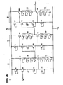
- an advantage of the amplifier configuration of the present invention is that a zero DC offset voltage is obtained by virtue of its symmetrical circuit arrangement. Therefore, a symmetric amplifier may be fabricated which exhibits a 0V DC offset, regardless of changes in supply voltage or transistor threshold voltage. With this ability to reproducibly provide a 0V DC offset, a multistage symmetric amplifier may be formed simply by connecting a number of single stage amplifiers together in series. One such multistage symmetric amplifier is illustrated in FIG. 4.
- a multistage symmetric amplifier 50 which includes a first (or input) stage 52, a second stage 54, and a third (or output) stage 56.
- Each stage is identical in design to amplifier 30 of FIG. 1, where only the size of the various FETs used to form each stage may be altered to provide different impedance levels at each stage.
- first stage 52 includes an input FET 60 which is coupled at its gate to the input voltage signal V IN .
- An active load FET 62 is coupled as shown between power supply VDD and the drain of FET 60.
- Impedance matching elements 64 and 66 are included in the input branch of first stage 52 between the source of input FET 60 and the second power supply VSS.
- elements 64 and 66 are sized to provide a gate bias to FET 72 which is substantially equal to the bias applied to buffer FET 68.
- impedance matching elements 64 and 66 comprise active load elements, formed by a pair of gate-source coupled FETs, connected in series between the source of input FET 60 and VSS. As in FIG. 3, resistors may be substituted for these FETs.
- first diode level shifting arrangement 70 (illustrated in FIG. 4 as consisting of three source-drain coupled FETs) is connected between the source of first buffer FET 68 and the output of first stage 52 (denoted as C1 in FIG. 4).
- the symmetry in first stage 52 is provided by a second buffer FET 72 and second diode level shifting arrangement 74 connected in series between output node C1 and VSS.
- second buffer FET In order to preserve the symmetry, second buffer FET must be identical (in size) to buffer FET 68. Additionally, second diode level shifting arrangement 74 must comprise the same number of source-drain coupled FETs as first arrangement 70.
- the output from first stage 52 is directly connected to the input of second stage 54. That is, the drain of second buffer FET 72 is directly connected to the gate of input FET 76 of second stage 54.
- Second stage 54 further includes in its input branch an active load FET 78 and active load impedance matching elements 80,82 (illustrated as gate-source coupled FETs).
- the output branch of second stage 54 includes a first buffer FET 84 coupled at its gate to the drain of input FET 76, and a first diode level shifting arrangement 86 comprising a series of three source-drain coupled FETs.
- second buffer FET 88 and second diode level shifting arrangement 90 fabricated to match first buffer FET 84 and first diode arrangement 86, respectively.
- the output from second stage 54 is then directly connected to the input of third stage 56, the gate of input FET 92.
- Third stage 56 comprises an active load FET 94, impedance matching FETs 96,98, first and second buffer FETs 100,104, and first and second diode level shifting arrangements 102, 106, where all of these devices function as described above.
- the output from third stage 56 is thus the final amplified output signal V OUT from multistage amplifier 50, where the amount of gain imposed on signal V OUT will be a function of the gain provided by each stage.
Landscapes
- Engineering & Computer Science (AREA)
- Power Engineering (AREA)
- Amplifiers (AREA)
- Manipulation Of Pulses (AREA)
Applications Claiming Priority (2)
| Application Number | Priority Date | Filing Date | Title |
|---|---|---|---|
| US209462 | 1988-06-20 | ||
| US07/209,462 US4825174A (en) | 1988-06-20 | 1988-06-20 | Symmetric integrated amplifier with controlled DC offset voltage |
Publications (3)
| Publication Number | Publication Date |
|---|---|
| EP0348079A2 true EP0348079A2 (de) | 1989-12-27 |
| EP0348079A3 EP0348079A3 (en) | 1990-08-22 |
| EP0348079B1 EP0348079B1 (de) | 1993-05-19 |
Family
ID=22778845
Family Applications (1)
| Application Number | Title | Priority Date | Filing Date |
|---|---|---|---|
| EP89305852A Expired - Lifetime EP0348079B1 (de) | 1988-06-20 | 1989-06-09 | Symmetrischer integrierter Verstärker mit gesteuerter Offset-Gleichspannung |
Country Status (7)
| Country | Link |
|---|---|
| US (1) | US4825174A (de) |
| EP (1) | EP0348079B1 (de) |
| JP (1) | JPH07120904B2 (de) |
| KR (1) | KR920010005B1 (de) |
| CA (1) | CA1289205C (de) |
| DE (1) | DE68906601T2 (de) |
| ES (1) | ES2041414T3 (de) |
Families Citing this family (22)
| Publication number | Priority date | Publication date | Assignee | Title |
|---|---|---|---|---|
| US5502735A (en) * | 1991-07-16 | 1996-03-26 | Nokia Mobile Phones (U.K.) Limited | Maximum likelihood sequence detector |
| KR940004430B1 (ko) * | 1991-11-01 | 1994-05-25 | 한국전기통신공사 | Mosfet 저항성 제어형 곱셈연산기 |
| DE19534065A1 (de) * | 1995-09-14 | 1996-07-04 | Telefunken Microelectron | Spannungsverstärkerstufe |
| US6566936B1 (en) * | 1999-10-29 | 2003-05-20 | Lovoltech Inc. | Two terminal rectifier normally OFF JFET |
| US6580326B2 (en) * | 2001-05-25 | 2003-06-17 | Infineon Technologies North America Corp. | High-bandwidth low-voltage gain cell and voltage follower having an enhanced transconductance |
| US7034608B2 (en) * | 2004-02-20 | 2006-04-25 | Fujitsu Limited | Correcting DC offsets in a multi-stage amplifier |
| US20070096821A1 (en) * | 2005-11-03 | 2007-05-03 | Samsung Electronics Co., Ltd. | Wide-band amplifier |
| KR20070114557A (ko) * | 2006-05-29 | 2007-12-04 | 삼성전자주식회사 | 퓨즈를 갖는 반도체 기억 소자 및 그 형성 방법 |
| US7817757B2 (en) * | 2006-05-30 | 2010-10-19 | Fujitsu Limited | System and method for independently adjusting multiple offset compensations applied to a signal |
| US7839958B2 (en) | 2006-05-30 | 2010-11-23 | Fujitsu Limited | System and method for the adjustment of compensation applied to a signal |
| US7848470B2 (en) * | 2006-05-30 | 2010-12-07 | Fujitsu Limited | System and method for asymmetrically adjusting compensation applied to a signal |
| US7804894B2 (en) | 2006-05-30 | 2010-09-28 | Fujitsu Limited | System and method for the adjustment of compensation applied to a signal using filter patterns |
| US7804921B2 (en) | 2006-05-30 | 2010-09-28 | Fujitsu Limited | System and method for decoupling multiple control loops |
| US7801208B2 (en) * | 2006-05-30 | 2010-09-21 | Fujitsu Limited | System and method for adjusting compensation applied to a signal using filter patterns |
| US7760798B2 (en) * | 2006-05-30 | 2010-07-20 | Fujitsu Limited | System and method for adjusting compensation applied to a signal |
| US7764757B2 (en) * | 2006-05-30 | 2010-07-27 | Fujitsu Limited | System and method for the adjustment of offset compensation applied to a signal |
| US7787534B2 (en) * | 2006-05-30 | 2010-08-31 | Fujitsu Limited | System and method for adjusting offset compensation applied to a signal |
| US7839955B2 (en) * | 2006-05-30 | 2010-11-23 | Fujitsu Limited | System and method for the non-linear adjustment of compensation applied to a signal |
| US7817712B2 (en) * | 2006-05-30 | 2010-10-19 | Fujitsu Limited | System and method for independently adjusting multiple compensations applied to a signal |
| JP2008205827A (ja) * | 2007-02-20 | 2008-09-04 | Fujitsu Ltd | 増幅回路 |
| US9354649B2 (en) * | 2014-02-03 | 2016-05-31 | Qualcomm, Incorporated | Buffer circuit for a LDO regulator |
| TWI750697B (zh) * | 2020-06-17 | 2021-12-21 | 正基科技股份有限公司 | 共振本體與功率分割合併器 |
Family Cites Families (6)
| Publication number | Priority date | Publication date | Assignee | Title |
|---|---|---|---|---|
| JPS59186410A (ja) * | 1983-04-08 | 1984-10-23 | Fujitsu Ltd | 帰還型増幅器 |
| US4646028A (en) * | 1984-08-27 | 1987-02-24 | Texas Instruments Incorporated | GaAs monolithic medium power amplifier |
| US4616189A (en) * | 1985-04-26 | 1986-10-07 | Triquint Semiconductor, Inc. | Gallium arsenide differential amplifier with closed loop bias stabilization |
| US4634993A (en) * | 1985-08-23 | 1987-01-06 | Burr-Brown Corporation | High gain, low drift operational amplifier for sample and hold circuit |
| US4743862A (en) * | 1986-05-02 | 1988-05-10 | Anadigics, Inc. | JFET current mirror and voltage level shifting apparatus |
| US4767946A (en) * | 1987-01-12 | 1988-08-30 | Tektronix, Inc. | High-speed supply independent level shifter |
-
1988
- 1988-06-20 US US07/209,462 patent/US4825174A/en not_active Expired - Lifetime
-
1989
- 1989-05-29 CA CA000600924A patent/CA1289205C/en not_active Expired - Fee Related
- 1989-06-09 DE DE89305852T patent/DE68906601T2/de not_active Expired - Fee Related
- 1989-06-09 EP EP89305852A patent/EP0348079B1/de not_active Expired - Lifetime
- 1989-06-09 ES ES198989305852T patent/ES2041414T3/es not_active Expired - Lifetime
- 1989-06-16 JP JP1154419A patent/JPH07120904B2/ja not_active Expired - Fee Related
- 1989-06-16 KR KR1019890008300A patent/KR920010005B1/ko not_active Expired
Also Published As
| Publication number | Publication date |
|---|---|
| US4825174A (en) | 1989-04-25 |
| DE68906601D1 (de) | 1993-06-24 |
| JPH0239707A (ja) | 1990-02-08 |
| CA1289205C (en) | 1991-09-17 |
| KR900001113A (ko) | 1990-01-31 |
| EP0348079A3 (en) | 1990-08-22 |
| ES2041414T3 (es) | 1993-11-16 |
| EP0348079B1 (de) | 1993-05-19 |
| KR920010005B1 (ko) | 1992-11-10 |
| DE68906601T2 (de) | 1993-12-23 |
| JPH07120904B2 (ja) | 1995-12-20 |
Similar Documents
| Publication | Publication Date | Title |
|---|---|---|
| EP0348079B1 (de) | Symmetrischer integrierter Verstärker mit gesteuerter Offset-Gleichspannung | |
| US4616189A (en) | Gallium arsenide differential amplifier with closed loop bias stabilization | |
| US4626770A (en) | NPN band gap voltage reference | |
| US5892400A (en) | Amplifier using a single polarity power supply and including depletion mode FET and negative voltage generator | |
| US5381112A (en) | Fully differential line driver circuit having common-mode feedback | |
| EP0594305B1 (de) | Vergleichsschaltung | |
| CA1210085A (en) | Level shifting circuit | |
| EP0488315B1 (de) | Symmetrischer Kaskodenstromspiegel | |
| WO1990006626A1 (en) | Single input to differential output amplifier | |
| KR950003140B1 (ko) | 증폭회로 | |
| US4737732A (en) | Low voltage operational amplifier having a substantially full range output voltage | |
| US4460874A (en) | Three-terminal operational amplifier/comparator with offset compensation | |
| JP3139868B2 (ja) | 入力回路 | |
| JPH07202668A (ja) | 光受信器装置 | |
| EP0579751B1 (de) | Transimpedanz-differenzverstärker | |
| US4933643A (en) | Operational amplifier having improved digitally adjusted null offset | |
| US5374859A (en) | Low power dual power supply high resolution comparator | |
| US6567441B2 (en) | Source follower circuit, laser driving apparatus, semiconductor laser apparatus, current-voltage convertion circuit, and light receiving circuit | |
| US4749955A (en) | Low voltage comparator circuit | |
| US4636654A (en) | GaAs differential line receiver with positive feedback | |
| US4910472A (en) | Multivibrator circuit employing field effect devices | |
| US5107144A (en) | Integrated circuit having field effect transistors | |
| US4780687A (en) | Differential amplifier circuit for regenerating low-amplitude complementary signals | |
| US5012134A (en) | DC bootstrapped unity gain buffer | |
| US20030006842A1 (en) | Split cascode driver |
Legal Events
| Date | Code | Title | Description |
|---|---|---|---|
| PUAI | Public reference made under article 153(3) epc to a published international application that has entered the european phase |
Free format text: ORIGINAL CODE: 0009012 |
|
| AK | Designated contracting states |
Kind code of ref document: A2 Designated state(s): DE ES FR GB NL SE |
|
| PUAL | Search report despatched |
Free format text: ORIGINAL CODE: 0009013 |
|
| AK | Designated contracting states |
Kind code of ref document: A3 Designated state(s): DE ES FR GB NL SE |
|
| 17P | Request for examination filed |
Effective date: 19901211 |
|
| 17Q | First examination report despatched |
Effective date: 19920713 |
|
| GRAA | (expected) grant |
Free format text: ORIGINAL CODE: 0009210 |
|
| AK | Designated contracting states |
Kind code of ref document: B1 Designated state(s): DE ES FR GB NL SE |
|
| REF | Corresponds to: |
Ref document number: 68906601 Country of ref document: DE Date of ref document: 19930624 |
|
| ET | Fr: translation filed | ||
| REG | Reference to a national code |
Ref country code: ES Ref legal event code: FG2A Ref document number: 2041414 Country of ref document: ES Kind code of ref document: T3 |
|
| PLBE | No opposition filed within time limit |
Free format text: ORIGINAL CODE: 0009261 |
|
| STAA | Information on the status of an ep patent application or granted ep patent |
Free format text: STATUS: NO OPPOSITION FILED WITHIN TIME LIMIT |
|
| 26N | No opposition filed | ||
| EAL | Se: european patent in force in sweden |
Ref document number: 89305852.9 |
|
| PGFP | Annual fee paid to national office [announced via postgrant information from national office to epo] |
Ref country code: SE Payment date: 20000327 Year of fee payment: 12 |
|
| PGFP | Annual fee paid to national office [announced via postgrant information from national office to epo] |
Ref country code: NL Payment date: 20000524 Year of fee payment: 12 |
|
| PGFP | Annual fee paid to national office [announced via postgrant information from national office to epo] |
Ref country code: GB Payment date: 20000525 Year of fee payment: 12 Ref country code: FR Payment date: 20000525 Year of fee payment: 12 |
|
| PGFP | Annual fee paid to national office [announced via postgrant information from national office to epo] |
Ref country code: ES Payment date: 20000602 Year of fee payment: 12 |
|
| PGFP | Annual fee paid to national office [announced via postgrant information from national office to epo] |
Ref country code: DE Payment date: 20000630 Year of fee payment: 12 |
|
| PG25 | Lapsed in a contracting state [announced via postgrant information from national office to epo] |
Ref country code: GB Free format text: LAPSE BECAUSE OF NON-PAYMENT OF DUE FEES Effective date: 20010609 |
|
| PG25 | Lapsed in a contracting state [announced via postgrant information from national office to epo] |
Ref country code: SE Free format text: LAPSE BECAUSE OF NON-PAYMENT OF DUE FEES Effective date: 20010610 Ref country code: ES Free format text: LAPSE BECAUSE OF NON-PAYMENT OF DUE FEES Effective date: 20010610 |
|
| PG25 | Lapsed in a contracting state [announced via postgrant information from national office to epo] |
Ref country code: NL Free format text: LAPSE BECAUSE OF NON-PAYMENT OF DUE FEES Effective date: 20020101 |
|
| GBPC | Gb: european patent ceased through non-payment of renewal fee |
Effective date: 20010609 |
|
| EUG | Se: european patent has lapsed |
Ref document number: 89305852.9 |
|
| PG25 | Lapsed in a contracting state [announced via postgrant information from national office to epo] |
Ref country code: FR Free format text: LAPSE BECAUSE OF NON-PAYMENT OF DUE FEES Effective date: 20020228 |
|
| NLV4 | Nl: lapsed or anulled due to non-payment of the annual fee |
Effective date: 20020101 |
|
| PG25 | Lapsed in a contracting state [announced via postgrant information from national office to epo] |
Ref country code: DE Free format text: LAPSE BECAUSE OF NON-PAYMENT OF DUE FEES Effective date: 20020403 |
|
| REG | Reference to a national code |
Ref country code: ES Ref legal event code: FD2A Effective date: 20020711 |