EP0347770B1 - Fabrication d'un oxyde supraconducteur de la famille du bismuth - Google Patents
Fabrication d'un oxyde supraconducteur de la famille du bismuth Download PDFInfo
- Publication number
- EP0347770B1 EP0347770B1 EP89110957A EP89110957A EP0347770B1 EP 0347770 B1 EP0347770 B1 EP 0347770B1 EP 89110957 A EP89110957 A EP 89110957A EP 89110957 A EP89110957 A EP 89110957A EP 0347770 B1 EP0347770 B1 EP 0347770B1
- Authority
- EP
- European Patent Office
- Prior art keywords
- sintering
- process according
- phase
- bismuth system
- system oxide
- Prior art date
- Legal status (The legal status is an assumption and is not a legal conclusion. Google has not performed a legal analysis and makes no representation as to the accuracy of the status listed.)
- Revoked
Links
- 229910052797 bismuth Inorganic materials 0.000 title claims abstract description 68
- JCXGWMGPZLAOME-UHFFFAOYSA-N bismuth atom Chemical compound [Bi] JCXGWMGPZLAOME-UHFFFAOYSA-N 0.000 title claims abstract description 67
- 238000000034 method Methods 0.000 title claims abstract description 19
- 239000002887 superconductor Substances 0.000 title claims abstract description 16
- 238000005245 sintering Methods 0.000 claims abstract description 48
- 239000000203 mixture Substances 0.000 claims abstract description 38
- 238000002156 mixing Methods 0.000 claims abstract description 5
- 239000005749 Copper compound Substances 0.000 claims abstract description 4
- 150000001880 copper compounds Chemical class 0.000 claims abstract description 4
- 150000001622 bismuth compounds Chemical class 0.000 claims abstract description 3
- 229940043430 calcium compound Drugs 0.000 claims abstract description 3
- 150000001674 calcium compounds Chemical class 0.000 claims abstract description 3
- 150000003438 strontium compounds Chemical class 0.000 claims abstract description 3
- 150000002611 lead compounds Chemical class 0.000 claims abstract 2
- 229910052760 oxygen Inorganic materials 0.000 claims description 44
- 239000001301 oxygen Substances 0.000 claims description 44
- 238000002844 melting Methods 0.000 claims description 17
- 230000008018 melting Effects 0.000 claims description 17
- 230000000694 effects Effects 0.000 claims description 14
- 150000002823 nitrates Chemical class 0.000 claims description 12
- 150000001875 compounds Chemical class 0.000 claims description 7
- 238000001816 cooling Methods 0.000 claims description 7
- 229910002651 NO3 Inorganic materials 0.000 claims description 2
- NHNBFGGVMKEFGY-UHFFFAOYSA-N Nitrate Chemical compound [O-][N+]([O-])=O NHNBFGGVMKEFGY-UHFFFAOYSA-N 0.000 claims description 2
- QVGXLLKOCUKJST-UHFFFAOYSA-N atomic oxygen Chemical compound [O] QVGXLLKOCUKJST-UHFFFAOYSA-N 0.000 claims 4
- 238000000354 decomposition reaction Methods 0.000 claims 2
- XTVVROIMIGLXTD-UHFFFAOYSA-N copper(II) nitrate Chemical compound [Cu+2].[O-][N+]([O-])=O.[O-][N+]([O-])=O XTVVROIMIGLXTD-UHFFFAOYSA-N 0.000 claims 1
- 238000005979 thermal decomposition reaction Methods 0.000 claims 1
- MYMOFIZGZYHOMD-UHFFFAOYSA-N Dioxygen Chemical compound O=O MYMOFIZGZYHOMD-UHFFFAOYSA-N 0.000 description 43
- 239000000463 material Substances 0.000 description 23
- 239000010949 copper Substances 0.000 description 22
- 238000002441 X-ray diffraction Methods 0.000 description 21
- 239000011575 calcium Substances 0.000 description 21
- XKRFYHLGVUSROY-UHFFFAOYSA-N Argon Chemical compound [Ar] XKRFYHLGVUSROY-UHFFFAOYSA-N 0.000 description 18
- 239000000523 sample Substances 0.000 description 16
- VTYYLEPIZMXCLO-UHFFFAOYSA-L Calcium carbonate Chemical compound [Ca+2].[O-]C([O-])=O VTYYLEPIZMXCLO-UHFFFAOYSA-L 0.000 description 14
- QPLDLSVMHZLSFG-UHFFFAOYSA-N Copper oxide Chemical compound [Cu]=O QPLDLSVMHZLSFG-UHFFFAOYSA-N 0.000 description 14
- WMWLMWRWZQELOS-UHFFFAOYSA-N bismuth(iii) oxide Chemical compound O=[Bi]O[Bi]=O WMWLMWRWZQELOS-UHFFFAOYSA-N 0.000 description 14
- 239000002994 raw material Substances 0.000 description 14
- 230000000052 comparative effect Effects 0.000 description 11
- 229910052786 argon Inorganic materials 0.000 description 9
- 238000010438 heat treatment Methods 0.000 description 9
- VYPSYNLAJGMNEJ-UHFFFAOYSA-N Silicium dioxide Chemical compound O=[Si]=O VYPSYNLAJGMNEJ-UHFFFAOYSA-N 0.000 description 8
- 230000007423 decrease Effects 0.000 description 8
- 239000012535 impurity Substances 0.000 description 8
- 239000004570 mortar (masonry) Substances 0.000 description 8
- GRYLNZFGIOXLOG-UHFFFAOYSA-N Nitric acid Chemical compound O[N+]([O-])=O GRYLNZFGIOXLOG-UHFFFAOYSA-N 0.000 description 7
- 229910000019 calcium carbonate Inorganic materials 0.000 description 7
- 235000010216 calcium carbonate Nutrition 0.000 description 7
- 229910017604 nitric acid Inorganic materials 0.000 description 7
- LEDMRZGFZIAGGB-UHFFFAOYSA-L strontium carbonate Chemical compound [Sr+2].[O-]C([O-])=O LEDMRZGFZIAGGB-UHFFFAOYSA-L 0.000 description 7
- 229910000018 strontium carbonate Inorganic materials 0.000 description 7
- XLYOFNOQVPJJNP-UHFFFAOYSA-N water Substances O XLYOFNOQVPJJNP-UHFFFAOYSA-N 0.000 description 7
- PNEYBMLMFCGWSK-UHFFFAOYSA-N aluminium oxide Inorganic materials [O-2].[O-2].[O-2].[Al+3].[Al+3] PNEYBMLMFCGWSK-UHFFFAOYSA-N 0.000 description 6
- BASFCYQUMIYNBI-UHFFFAOYSA-N platinum Chemical compound [Pt] BASFCYQUMIYNBI-UHFFFAOYSA-N 0.000 description 6
- 125000004429 atom Chemical group 0.000 description 5
- 238000001704 evaporation Methods 0.000 description 5
- HTUMBQDCCIXGCV-UHFFFAOYSA-N lead oxide Chemical compound [O-2].[Pb+2] HTUMBQDCCIXGCV-UHFFFAOYSA-N 0.000 description 5
- YEXPOXQUZXUXJW-UHFFFAOYSA-N lead(II) oxide Inorganic materials [Pb]=O YEXPOXQUZXUXJW-UHFFFAOYSA-N 0.000 description 5
- 230000015572 biosynthetic process Effects 0.000 description 4
- 229910052802 copper Inorganic materials 0.000 description 4
- 238000003756 stirring Methods 0.000 description 4
- RYGMFSIKBFXOCR-UHFFFAOYSA-N Copper Chemical compound [Cu] RYGMFSIKBFXOCR-UHFFFAOYSA-N 0.000 description 3
- 229910002480 Cu-O Inorganic materials 0.000 description 3
- 229910052791 calcium Inorganic materials 0.000 description 3
- 239000011261 inert gas Substances 0.000 description 3
- 229910052697 platinum Inorganic materials 0.000 description 3
- 229910052712 strontium Inorganic materials 0.000 description 3
- IJGRMHOSHXDMSA-UHFFFAOYSA-N Atomic nitrogen Chemical compound N#N IJGRMHOSHXDMSA-UHFFFAOYSA-N 0.000 description 2
- OYPRJOBELJOOCE-UHFFFAOYSA-N Calcium Chemical compound [Ca] OYPRJOBELJOOCE-UHFFFAOYSA-N 0.000 description 2
- 150000004649 carbonic acid derivatives Chemical class 0.000 description 2
- 238000007796 conventional method Methods 0.000 description 2
- 239000013078 crystal Substances 0.000 description 2
- 230000003247 decreasing effect Effects 0.000 description 2
- 230000008020 evaporation Effects 0.000 description 2
- 238000000227 grinding Methods 0.000 description 2
- -1 oxides Chemical class 0.000 description 2
- 238000002360 preparation method Methods 0.000 description 2
- 238000004544 sputter deposition Methods 0.000 description 2
- CIOAGBVUUVVLOB-UHFFFAOYSA-N strontium atom Chemical compound [Sr] CIOAGBVUUVVLOB-UHFFFAOYSA-N 0.000 description 2
- 239000010409 thin film Substances 0.000 description 2
- XUIMIQQOPSSXEZ-UHFFFAOYSA-N Silicon Chemical compound [Si] XUIMIQQOPSSXEZ-UHFFFAOYSA-N 0.000 description 1
- 150000001242 acetic acid derivatives Chemical class 0.000 description 1
- 150000001621 bismuth Chemical class 0.000 description 1
- 239000000919 ceramic Substances 0.000 description 1
- 238000006243 chemical reaction Methods 0.000 description 1
- 238000001514 detection method Methods 0.000 description 1
- 229910001882 dioxygen Inorganic materials 0.000 description 1
- 239000006185 dispersion Substances 0.000 description 1
- 239000001307 helium Substances 0.000 description 1
- 229910052734 helium Inorganic materials 0.000 description 1
- SWQJXJOGLNCZEY-UHFFFAOYSA-N helium atom Chemical compound [He] SWQJXJOGLNCZEY-UHFFFAOYSA-N 0.000 description 1
- RXPAJWPEYBDXOG-UHFFFAOYSA-N hydron;methyl 4-methoxypyridine-2-carboxylate;chloride Chemical compound Cl.COC(=O)C1=CC(OC)=CC=N1 RXPAJWPEYBDXOG-UHFFFAOYSA-N 0.000 description 1
- 150000004679 hydroxides Chemical class 0.000 description 1
- 150000002484 inorganic compounds Chemical class 0.000 description 1
- 229910010272 inorganic material Inorganic materials 0.000 description 1
- 229910052745 lead Inorganic materials 0.000 description 1
- 230000005415 magnetization Effects 0.000 description 1
- 238000004519 manufacturing process Methods 0.000 description 1
- 238000005259 measurement Methods 0.000 description 1
- 230000007246 mechanism Effects 0.000 description 1
- 239000000289 melt material Substances 0.000 description 1
- 229910052751 metal Inorganic materials 0.000 description 1
- 239000002184 metal Substances 0.000 description 1
- 150000002739 metals Chemical class 0.000 description 1
- 238000012544 monitoring process Methods 0.000 description 1
- 229910052757 nitrogen Inorganic materials 0.000 description 1
- 150000003891 oxalate salts Chemical class 0.000 description 1
- 125000004430 oxygen atom Chemical group O* 0.000 description 1
- 239000008188 pellet Substances 0.000 description 1
- 239000000843 powder Substances 0.000 description 1
- 230000035484 reaction time Effects 0.000 description 1
- 239000004065 semiconductor Substances 0.000 description 1
- 229910052710 silicon Inorganic materials 0.000 description 1
- 239000010703 silicon Substances 0.000 description 1
- 239000007921 spray Substances 0.000 description 1
- 239000000758 substrate Substances 0.000 description 1
- 238000003786 synthesis reaction Methods 0.000 description 1
- 238000005303 weighing Methods 0.000 description 1
Images


Classifications
-
- H—ELECTRICITY
- H10—SEMICONDUCTOR DEVICES; ELECTRIC SOLID-STATE DEVICES NOT OTHERWISE PROVIDED FOR
- H10N—ELECTRIC SOLID-STATE DEVICES NOT OTHERWISE PROVIDED FOR
- H10N60/00—Superconducting devices
- H10N60/01—Manufacture or treatment
- H10N60/0268—Manufacture or treatment of devices comprising copper oxide
-
- C—CHEMISTRY; METALLURGY
- C04—CEMENTS; CONCRETE; ARTIFICIAL STONE; CERAMICS; REFRACTORIES
- C04B—LIME, MAGNESIA; SLAG; CEMENTS; COMPOSITIONS THEREOF, e.g. MORTARS, CONCRETE OR LIKE BUILDING MATERIALS; ARTIFICIAL STONE; CERAMICS; REFRACTORIES; TREATMENT OF NATURAL STONE
- C04B35/00—Shaped ceramic products characterised by their composition; Ceramics compositions; Processing powders of inorganic compounds preparatory to the manufacturing of ceramic products
- C04B35/01—Shaped ceramic products characterised by their composition; Ceramics compositions; Processing powders of inorganic compounds preparatory to the manufacturing of ceramic products based on oxide ceramics
- C04B35/45—Shaped ceramic products characterised by their composition; Ceramics compositions; Processing powders of inorganic compounds preparatory to the manufacturing of ceramic products based on oxide ceramics based on copper oxide or solid solutions thereof with other oxides
- C04B35/4521—Shaped ceramic products characterised by their composition; Ceramics compositions; Processing powders of inorganic compounds preparatory to the manufacturing of ceramic products based on oxide ceramics based on copper oxide or solid solutions thereof with other oxides containing bismuth oxide
- C04B35/4525—Shaped ceramic products characterised by their composition; Ceramics compositions; Processing powders of inorganic compounds preparatory to the manufacturing of ceramic products based on oxide ceramics based on copper oxide or solid solutions thereof with other oxides containing bismuth oxide also containing lead oxide
-
- H—ELECTRICITY
- H10—SEMICONDUCTOR DEVICES; ELECTRIC SOLID-STATE DEVICES NOT OTHERWISE PROVIDED FOR
- H10N—ELECTRIC SOLID-STATE DEVICES NOT OTHERWISE PROVIDED FOR
- H10N60/00—Superconducting devices
- H10N60/80—Constructional details
- H10N60/85—Superconducting active materials
- H10N60/855—Ceramic superconductors
- H10N60/857—Ceramic superconductors comprising copper oxide
-
- Y—GENERAL TAGGING OF NEW TECHNOLOGICAL DEVELOPMENTS; GENERAL TAGGING OF CROSS-SECTIONAL TECHNOLOGIES SPANNING OVER SEVERAL SECTIONS OF THE IPC; TECHNICAL SUBJECTS COVERED BY FORMER USPC CROSS-REFERENCE ART COLLECTIONS [XRACs] AND DIGESTS
- Y02—TECHNOLOGIES OR APPLICATIONS FOR MITIGATION OR ADAPTATION AGAINST CLIMATE CHANGE
- Y02E—REDUCTION OF GREENHOUSE GAS [GHG] EMISSIONS, RELATED TO ENERGY GENERATION, TRANSMISSION OR DISTRIBUTION
- Y02E40/00—Technologies for an efficient electrical power generation, transmission or distribution
- Y02E40/60—Superconducting electric elements or equipment; Power systems integrating superconducting elements or equipment
-
- Y—GENERAL TAGGING OF NEW TECHNOLOGICAL DEVELOPMENTS; GENERAL TAGGING OF CROSS-SECTIONAL TECHNOLOGIES SPANNING OVER SEVERAL SECTIONS OF THE IPC; TECHNICAL SUBJECTS COVERED BY FORMER USPC CROSS-REFERENCE ART COLLECTIONS [XRACs] AND DIGESTS
- Y10—TECHNICAL SUBJECTS COVERED BY FORMER USPC
- Y10S—TECHNICAL SUBJECTS COVERED BY FORMER USPC CROSS-REFERENCE ART COLLECTIONS [XRACs] AND DIGESTS
- Y10S505/00—Superconductor technology: apparatus, material, process
- Y10S505/725—Process of making or treating high tc, above 30 k, superconducting shaped material, article, or device
- Y10S505/737—From inorganic salt precursors, e.g. nitrates
-
- Y—GENERAL TAGGING OF NEW TECHNOLOGICAL DEVELOPMENTS; GENERAL TAGGING OF CROSS-SECTIONAL TECHNOLOGIES SPANNING OVER SEVERAL SECTIONS OF THE IPC; TECHNICAL SUBJECTS COVERED BY FORMER USPC CROSS-REFERENCE ART COLLECTIONS [XRACs] AND DIGESTS
- Y10—TECHNICAL SUBJECTS COVERED BY FORMER USPC
- Y10S—TECHNICAL SUBJECTS COVERED BY FORMER USPC CROSS-REFERENCE ART COLLECTIONS [XRACs] AND DIGESTS
- Y10S505/00—Superconductor technology: apparatus, material, process
- Y10S505/775—High tc, above 30 k, superconducting material
- Y10S505/776—Containing transition metal oxide with rare earth or alkaline earth
- Y10S505/782—Bismuth-, e.g. BiCaSrCuO
Definitions
- the present invention relates to bismuth system oxide superconductors and preparation thereof. More particularly, the present invention relates to bismuth system oxide superconductors comprising the 110 K phase.
- the bismuth system oxide superconductor was found in January 1988 by Maeda et al (Jap. J. Appl. Phys., 27, (1988) L209). With this bismuth system oxide, sharp decrease of electric resistance was observed around 110 K and also the Meissner effect was observed in the same temperature range. Since the critical temperature of 110 K is much higher than 90 K of YBa2CU3O y which had been believed to have the highest critical temperature, the bismuth system oxide is expected to find various applications in future.
- a phase of the bismuth system oxide having the critical temperature of 110 K can be isolated as a single crystal.
- the isolated single crystal cannot be used as a superconductive material.
- impurities such as a 80 K phase or a semiconductive phase and Ca2PbO4.
- the X-ray diffraction pattern of the bismuth system oxide had weak diffraction peaks other than that assigned to the 110 K phase, although compounds to which such weak diffraction peaks are assigned were not specified. Since the presence of several phases in the material seriously deteriorates the superconductive properties, it was desired to provide a superconductive material essentially consisting of the 110 K phase.
- L 1041-1043) proposed the addition of lead (Pb), and Kijima (EP-0 359 827 A1) et al proposed the variation of the composition. Although they achieved some improvements, their process require long reaction time, for example, 244 hours in the air by Takano et al or 120 hours in the air by Kijima et al.
- the decrease of the reaction temperature is one of the important requirements.
- the oxide superconductor should be produced at a sintering temperature as low as possible so as not to deteriorate properties of silicon substrates.
- the bulk materials should be sintered at about 900°C and 1,000°C, respectively.
- the bismuth system oxide can be sintered at a comparatively low temperature, the sintering temperature is still about 870°C.
- One object of the present invention is to provide a process for effectively producing a bismuth system oxide having a larger proportion of the 110 K phase in a comparatively short time.
- Another object of the present invention is to provide a process for producing a bismuth system oxide superconductor in which a raw material mixture can be sintered at a comparatively low temperature.
- Another object of the present invention is to provide a bismuth system oxide superconductor consisting essentially of the 110 K phase.
- the present invention provides a process of producing a bismuth system oxide superconductor, which comprises mixing a bismuth compound, a strontium compound, a calcium compound and a copper compound characterized in sintering the mixture under atmospheric pressure wherein the oxygen partial pressure during sintering is not higher than 0.15 atm.
- the bismuth system oxide superconductor of the present invention comprises bismuth, strontium, calcium, copper and oxygen atoms. A part of the bismuth atoms may be replaced with lead atoms.
- the bismuth system oxide has different performances.
- the atomic ratio of Bi:Sr:Ca:Cu is 1:1:1:2, the proportion of the 110 K phase is maximum.
- the 80 K phase dominates in the bismuth system oxide.
- the atomic ratio of strontium to bismuth is from 0.8 to 1.2, that of calcium to bismuth is from 1 to 4, that of copper to bismuth is from 1.5 to 5.
- the atomic ratio of lead to bismuth is from 0.1:0.9 to 0.4:0.6.
- the bismuth system oxide superconductive material may include the 110 K phase, the 80 K phase and the semiconductive phase.
- diffraction lines to be assigned to the 110 K phase, the 80 K phase and the semiconductive phase appear at 2 ⁇ of about 4.7°, 5.7° and 7.2°, respectively.
- a diffraction line to be assigned to Ca2PbO4 which is contained as an impurity appears at 2 ⁇ of 17.8°.
- a weak diffraction line which may be assigned to other impurities may appear at 2 ⁇ of 16.5°.
- the bismuth system oxide preferably has the composition of Bi x Pb y (Sr u Ca v Cu w ) z O ⁇ wherein x is a number of from 0.150 to 0.215, y is a number of 0.030 to 0.090 and z is a number of 0.720 to 0.800 provided that the sum of x, y and z is 1 (one); and u is a number of from 0.200 to 0.290, v is a number of from 0.250 to 0.355 and w is a number of from 0.430 to 0.530 provided that the sum of u, v and w is 1 (one) and ⁇ is a number of 0.8 to 1.3.
- x is a number of from 0.185 to 0.210
- y is a number of 0.030 to 0.050 and z is a number of 0.750 to 0.770 provided that the sum of x, y and z is 1
- u is a number of from 0.255 to 0.290
- v is a number of from 0.275 to 0.310
- w is a number of from 0.430 to 0.455 provided that the sum of u, v and w is 1
- a is a number from 0.8 to 1.3.
- the bismuth system oxide superconductive material of the present invention includes a phase which becomes superconductive in a temperature range of 90 to 100 K (hereinafter referred to as "95 K phase").
- the diffraction line may appear at 2 ⁇ of 5.7° and/or 7.2°.
- the superconductive material may contain the impurities. Since the 95 K phase provides the diffraction line at 2 ⁇ of 4.7°, it is substantially the same as the 110 K phase from the view point of the X-ray diffraction pattern.
- the 110 K phase has a higher critical temperature but small critical current. Therefore, the critical temperature should be measured with a very small current. Otherwise, a tail appears in the lower temperature side and the apparent critical temperature is measured lower than the actual one.
- the 95 K phase has the lower critical temperature than the 110 K phase, the former has a strong pinning effect than the latter and therefore the former has the large critical current J c .
- the raw materials for supplying the above atoms in the bismuth system oxide may be any of inorganic compounds such as hydroxides, oxides, carbonates and nitrates and organic acid salts such as oxalates and acetates insofar as the compounds can be converted to the corresponding oxides by heating.
- at least copper is used in the form of its nitrate, more preferably, all the raw materials are in the form of nitrates.
- the carbonates or oxides may be dissolved in nitric acid.
- the raw materials are homogeneously mixed by any of the conventional methods.
- the raw materials are ground and mixed in a mortar made of agate or with a ball mill.
- the raw materials are dissolved or dispersed in water and heated to dryness while stirring. Since bismuth nitrate is hardly soluble in pure water, preferably water is acidified with nitric acid. Further, the solution or dispersion of the raw materials can be spray dried and mixed. Alternatively, a thin film formed by sputtering has a homogeneous composition.
- the raw material mixture prepared by the above methods is provisionally sintered before sintering, although the mixture may be sintered without provisional sintering.
- the mixture of the compounds other than oxides is provisionally sintered at a temperature around 800°C, for example from 800 to 840°C in an atmosphere of the air, oxygen or a mixture of oxygen and an inert gas (e.g. nitrogen, helium, argon, etc.). It is not necessary to provisionally sinter the mixture of oxides or the thin film of oxides or metals formed by sputtering before sintering.
- the raw materials are in the powder form, they are molded before sintering.
- the raw materials may be molded in any shape and/or size.
- the molded material may be in the form of a pellet, a thin plate or a wire.
- the sintering is carried out usually in the air.
- the partial pressure of oxygen may be from 0 (zero) to 0.015 MPa (0.15 atm), preferably from 0.003 MPa to 0.01 MPa (0.03 to 0.1 atm).
- the air or pure oxygen gas may be diluted with the inert gas.
- the oxygen partial pressure of 0 (zero) means that no oxygen is contained and the sintering atmosphere consists of pure inert gas.
- the sintering temperature varies with the oxygen partial pressure and/or the composition of the raw materials.
- the sintering temperature is from just below the melting point of the raw material to 50°C below said melting point, preferably 30°C below said melting point.
- the raw material cannot be reacted at a temperature higher than the melting point, since the once melt material has no superconductive property.
- the melting point is about 870°C under the oxygen partial pressure of 0.02 MPa (0.2 atm.)., about 850°C under oxygen partial pressure of 0.003 MPa (0.03 atm.), about 830°C under oxygen partial pressure of 0.001 MPa (0.01 atm)., or about 810°C under oxygen partial pressure of 0 (zero).
- the atomic ratio of Bi:Pb:Sr:Ca:Cu is 0.8:0.2:0.8:1:1.4
- the melting point under the oxygen partial pressure of 0.02 MPa (0.2 atm). is about 845°C.
- the sintering time is at least 2 hours, preferably at least 8 hours, more preferably at least 12 hours.
- the sintered oxide material is cooled preferably in an atmosphere having an oxygen partial pressure higher than that in the sintering step, while it may be cooled in the atmosphere having the same oxygen partial pressure as in the sintering step.
- an atmosphere having an oxygen partial pressure higher than that in the sintering step while it may be cooled in the atmosphere having the same oxygen partial pressure as in the sintering step.
- the bismuth system oxide cooled in the atmosphere having the higher oxygen partial pressure a larger amount of current can be flown.
- the 110 K phase and the 95 K phase can be clearly separated in the magnetization measurement by cooling under the higher oxygen partial pressure.
- the sintered oxide is cooled under the same oxygen partial pressure as in the sintering pressure, heated at a temperature lower than the sintering temperature and treated with oxygen under the higher oxygen pressure.
- Bi2O3, SrCO3, CaCO3 and CuO were weighed so that the atomic ratio of Bi:Sr:Ca:Cu was 1:1:1:2 and completely dissolved in excess nitric acid while heating.
- the solution was charged in an evaporating dish made of platinum and heated while continuous stirring to evaporate water off. During evaporation, excess nitric acid was also removed.
- the mixture of nitrates was taken in an alumina crucible and further heated, whereby the nitrates were decomposed to liberate NO2. The heating was continued at 800°C till no NO2 was liberated.
- the mixture was ground in an agate mortar and molded in a round plate of 13 mm in diameter and about 1 mm in thickness.
- the plate was placed in an alumina boat and set at the center of a tubular furnace of 100 mm in inner diameter and 600 mm in length. Then, the plate was sintered at 867°C for 12 hours with flowing a mixture of argon and oxygen in a volume ratio of 4:1 at a flow rate of 250 ml/min. The sintered plate was ground and re-molded in a round plate having the same sizes as above. Then, the plate was sintered for 12 hours under the same conditions as above.
- the sintered round plate was slightly warped. This indicated that the sintering was carried out just below the melting point. With this sintered sample, an X-ray diffraction pattern, electric resistance and the Meissner effect were measured.
- the resistance was measured on the sintered plate as such by the standard four probe method.
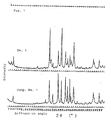
- the Meissner effect was measured at room temperature by placing the sample in a coil having an inductance of about 1.7 mH and monitoring the change of inductance. The results are shown in Figs. 1, 2 and 3, respectively.
- Fig. 1 the diffraction line assigned to the (002) plane of the 110 K phase appears around 2 ⁇ of 4.7°, and the diffraction line assigned to the 80 K phase appears around 2 ⁇ of 5.7°.
- Figs. 2 and 3 the resistance and the coil inductance change sharply drop around 110 K. This indicates the formation of the 110 K phase.
- Bi2O3, SrCO3, CaCO3 and CuO were weighed so that the atomic ratio of Bi:Sr:Ca:Cu was 1:1:1:2 and thoroughly mixed in the agate mortar. Then, the mixture was provisionally sintered at 810°C for 10 hours in a stream of air. Thereafter, the grinding and the three hour provisional sintering were repeated twice. The provisionally sintered material was again ground and molded to obtain a round plate of 13 mm in diameter and about 1 mm in thickness. Then, the plate was sintered under the same conditions as in Example 1.
- the sintered round plate was-slightly warped. This indicated that the sintering was carried out just below the melting point.
- an X-ray diffraction pattern, resistance and the Meissner effect were measured in the same manners as in Example 1. The results are also shown in Figs. 1, 2 and 3. In the X-ray diffraction pattern, only the diffraction line at 2 ⁇ of 5.7° appeared but no diffraction line at 2 ⁇ of 4.7° which is assigned to the 110 K phase appeared. The changes of the resistance and the inductance change near 110 K were slight, which indicates that the proportion of the 110 K phase was small.
- Nitrates of Bi, Pb, Sr, Ca and Cu were weighed so that the atomic ratio of Bi:Pb:Sr:Ca:Cu was 0.8:0.2:0.8: 1.0:1.4 and completely dissolved in water acidified with nitric acid.
- the solution was charged in an evaporating dish made of platinum and heated while continuously stirring to evaporate water off.
- the mixture of nitrates was taken in an alumina crucible and further heated, whereby the nitrates were decomposed to liberate NO2. The heating was continued at 800°C till no NO2 was liberated.
- the mixture was ground in an agate mortar and molded in a round plate of 13 mm in diameter and about 1 mm in thickness.
- the plate was placed in an alumina boat and set at the center of a tubular furnace of 100 mm in inner diameter and 600 mm in length. Then, the plate was sintered at 828°C for 12 hours with flowing a mixture of argon and oxygen in a volume ratio of 12:1 at a flow rate of 250 ml/min. The sintered plate was ground and re-molded in a round plate having the same sizes as above. Then, the plate was sintered for 108 hours under the same conditions as above.
- the sintered round plate was slightly warped. This indicated that the sintering was carried out just below the melting point.
- an X-ray diffraction pattern, electric resistance and the Meissner effect were measured in the same manners as in Example 1. The results are shown in Figs. 4, 5 and 6, respectively.
- the diffraction line at 2 ⁇ of 4.7° which is assigned to the 110 K phase appeared but no diffraction line was found at 2 ⁇ of 5.7°.
- the changes of the resistance and the coil inductance change near 110 K were considerably large, which indicates that the most portion of the sintered plate consisted of the 110 K phase.
- the intensity of diffraction line at 2 ⁇ of 5.7° was at most 15 % of that at 2 ⁇ of 4.7°.
- the intensity of the diffraction line is a distance from the base line to the top of the line.
- the plate was sintered in the same manner as in Example 1 but heating the plate at 861°C with flowing a mixture of argon and oxygen in a volume ratio of 12:1 (corresponding to the oxygen partial pressure of 0.0077 MPa (0.077 atm).) at a flow rate of 250 ml/min.
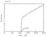
- the sintered round plate was slightly warped. This indicated that the sintering was carried out just below the melting point. With this sintered sample, the resistance and the Meissner effect were measured in the same manners as in Example 1. The results are shown in Figs. 7 and 8. The sharp changes of the resistance and the inductance change appeared around 110 K. This indicates the formation of the 110 K phase.
- the sintered round plate was slightly warped. This indicated that the sintering was carried out just below the melting point. With this sintered sample, the resistance was measured in the same manner as in Example 1. The result is shown in Fig. 7. The sharp change of the resistance appeared around 110 K. This indicates the formation of the 110 K phase.
- the 110 K phase can be formed at a temperature at which the 110 K phase was not formed by the conventional methods.
- the sintered round plate was not deformed since the sintering temperature was 15°C lower than the melting point.
- the resistance and coil inductance change of this sample are shown in Figs. 7 and 8.
- the steep decreases of the resistance and coil inductance change were observed around 110 K. It is clear that, according to the present invention, the 110 K phase is formed at a comparatively low sintering temperature of 816°C.
- the sintered round plate was slightly warped. This indicated that the sintering temperature was just below the melting point.
- the resistance and coil inductance change of the sample were measured in the same manners as in Example 1. The results are shown in Figs. 7 and 8. No decrease of the resistance and coil inductance change was observed around 110 K. As understood from these results, at the high oxygen partial pressure, no or few 110 K phase is created.
- the sintered round plate was slightly warped. This indicated that the sintering temperature was just below the melting point.
- the resistance and coil inductance change of the sample were measured in the same manners as in Example 1. The results are shown in Figs. 7 and 8. Slight decrease of the resistance and coil inductance change was observed around 110 K. As understood from these results, in spite of the high sintering temperature of 870°C, only a small portion of the 110 K phase is created.
- Bi2O3, PbO, SrCO3, CaCO3 and CuO were weighed so that the atomic ratio of Bi:Pb:Sr:Ca:Cu was 0.8:0.15:0.86: 0.86:1.33, which corresponds to Bi 0.2 Pb 0.038 -(Sr 0.281 Ca 0.281 Cu 0.438 ) 0.763 O ⁇ , and completely dissolved in excess nitric acid while heating.
- the solution was charged in an evaporating dish made of platinum and heated while continuously stirring to evaporate water off. In this evaporation, excess nitric acid was also removed.
- the mixture of nitrates was taken in an alumina crucible and further heated, whereby the nitrates were decomposed to liberate NO2. The heating was continued at 800°C till no NO2 was liberated.
- the mixture was ground in an agate mortar and molded in a round plate of 13 mm in diameter and about 1 mm in thickness.
- the plate was placed in an alumina boat and set at the center of a tubular furnace of 100 mm in inner diameter and 600 mm in length. Then, the plate was sintered at 835°C for 12 hours with flowing a mixture of argon and oxygen in a volume ratio of 12:1 at a flow rate of 250 ml/min. The sintered plate was cooled to room temperature, ground and re-molded in a round plate having the same sizes as above. Then, the plate was sintered for 72 hours under the same conditions as above. Thereafter, the plate was cooled at a cooling rate of about 2°C/min. When the temperature reached 750°C, the atmosphere was changed to pure oxygen and the plate was cooled to room temperature.
- the diffraction line appeared at 2 ⁇ of 4.7° and no diffraction line appeared at 2 ⁇ of 5.7° or 7.2°.
- the resistivity change indicates the presence of the 110 K phase alone.
- the Meissner effect curve of Fig. 11 has two signals corresponding to the 110 K and 95 K phases. These two phases were contained in the volume ratio of about 1:1 and occupied about 92 % of the whole volume. From these results, it can be concluded that the sample produced in this Example consisted of the 1:1 mixture of two kinds of superconductive materials both having the same structure, namely the triple Cu-O layered structure.
- the shielding effect curve in Fig. 11 should be noted. According to this result, the change of magnetic susceptibility due to the shielding effect was three times larger than that due to the Meissner effect, and such is significantly observed at 90 K or lower. This means that the 95 K phase has the larger shielding effect. This indicates that the pinning effect against the fluxoid quantum beam by the 95 K phase is much larger than that by the 110 K phase, which means the larger critical current.
- Bi2O3, PbO, SrCO3, CaCO3 and CuO were weighed so that the atomic ratio of Bi:Pb:Sr:Ca:Cu was 0.8:0.2:0.8: 1.0:2.0, which corresponds to Bi 0.167 Pb 0.042 - (Sr 0.211 Ca 0.263 Cu 0.526 ) 0.792 O ⁇ , and thoroughly mixed in the agate mortar.
- the mixture was provisionally sintered at 810°C for 10 hours. Thereafter, the grinding and the three hour provisional sintering were repeated twice.
- the provisionally sintered mixture was again ground and molded to obtain a round plate of 13 mm in diameter and about 1 mm in thickness.
- the plate was sintered in the same manner as in Example 1 but heating the plate at 842°C for 80 hours with flowing the mixture of argon and oxygen in the volume ratio of 12:1 at a flow rate of 250 ml/min.
- the sintered plate was gradually cooled to room temperature under oxygen partial pressure of 1/0.13 MPa (1/13 atm). at a cooling rate of about 2°C/min.
- the sintered round plate was slightly warped. This indicated that the sintering was carried out just below the melting point. With this sintered sample, an X-ray diffraction pattern, resistance and coil inductance change were measured in the same manners as above. The results are shown in Figs. 12, 13 and 14.
- the diffraction line appeared at 2 ⁇ of 4.7° but no diffraction line appeared at 2 ⁇ of 5.7 or 7.2°. That is, the ratio of the intensity of the diffraction line at 2 ⁇ of 5.7° or about 7.2 was 0 (zero) % of that at 2 ⁇ of 4.7°.
- the resistivity steeply decreased from 110 K and dropped to 0 (zero) at 107 K.
- the inductance change steeply decreased in the same temperature range.
- Bi2O3, PbO, SrCO3, CaCO3 and CuO were weighed so that the atomic ratio of Bi:Pb:Sr:Ca:Cu was 0.8:0.2:0.8: 1.0:1.4, which corresponds to Bi 0.190 Pb 0.048 - (Sr 0.250 Ca 0.313 Cu 0.438 ) 0.762 O ⁇ , and thoroughly mixed in the agate mortar.
- the mixture was sintered in the same manners as in Example 6 but adjusting the sintering temperature, the sintering time and oxygen partial pressure as indicated in Table 1 and keeping the same oxygen partial pressure during cooling.
- Fig. 15 The X-ray diffraction patterns of the samples obtained in Examples 8-10 are shown in Fig. 15. The diffraction line appeared at 2 ⁇ of 4.7° but no or very weak diffraction line appeared at 2 ⁇ of 5.7° or 7.2°. This indicates that the proportion of the 110 K phase or the 95 K phase was large in each sample.
- Bi2O3, PbO, SrCO3, CaCO3 and CuO were weighed so that the atomic ratio of Bi:Pb:Sr:Ca:Cu was 0.8:0.15:0.83: 0.89:1.33, which corresponds to Bi 0.2 Pb 0.0375 - (Sr 0.272 Ca 0.292 Cu 0.436 ) 0.7625 O ⁇ and thoroughly mixed in the agate mortar.
- the mixture was sintered in the same manners as in Example 6 but keeping the same oxygen partial pressure during cooling.
- the X-ray diffraction pattern of this sample is shown in Fig. 16.
- the strong diffraction line appeared at 2 ⁇ of 4.7° but no diffraction line appeared at 2 ⁇ of 5.7° or 7.2°. That is, the ratio of the intensity of the diffraction line at 2 ⁇ of 5.7° or 7.2° was 0 (zero) % of that at 2 ⁇ of 4.7°.
- a weak line appeared in the 2 ⁇ range of 17°-18°, which was assigned to impurities
- no diffraction line at 2 ⁇ of 17.8°, 16.5° or 29.9° which is to be assigned to impurities was found. This indicates that the sample of this Example would be a superconductive material consisting of the triple Cu-O layered structure.
- Example 16 In the same manner as in Example 7 except that the raw materials were weighed so that the material had the composition of Bi 0.200 Pb 0.037 (Sr 0.259 Ca 0.303 Cu 0.438 ) 0.763 O ⁇ (Example 16) or Bi 0.200 Pb 0.037 (Sr 0.245 Ca 0.330 Cu 0.425 ) 0.763 O ⁇ (Example 17), the bismuth system oxide material was prepared.
- Diffraction lines appeared at 2 ⁇ of 5.7° and 7.2° with the strength ratio of 2 % and 9 %, respectively to that of the diffraction line at 2 ⁇ of 4.7°. Despite of the appearance of the diffraction lines at 2 ⁇ of 5.7° and 7.2°s, no 80 K phase was identified from the resistance-temperature curve of Fig. 17. The reason for this may be the 110 K phase and the 95 K phase being linked continuously.
- the X-ray diffraction patterns of the samples are shown in Fig. 18.
- the strong diffraction line appeared at 2 ⁇ of 4.7°. Further, at 2 ⁇ of 5.7°, a diffraction line to be assigned to the 80 K phase as well as those assigned to the impurities appeared. This indicates that the prepared material did not consist of the triple Cu-O layered structure alone.
Landscapes
- Engineering & Computer Science (AREA)
- Chemical & Material Sciences (AREA)
- Ceramic Engineering (AREA)
- Manufacturing & Machinery (AREA)
- Materials Engineering (AREA)
- Structural Engineering (AREA)
- Organic Chemistry (AREA)
- Inorganic Compounds Of Heavy Metals (AREA)
- Compositions Of Oxide Ceramics (AREA)
- Superconductors And Manufacturing Methods Therefor (AREA)
Claims (11)
- Procédé de production d'un supraconducteur oxyde du système du bismuth qui comprend le mélange d'un composé du bismuth, d'un composé du strontium, d'un composé du calcium et d'un composé du cuivre, caractérisé par le frittage du mélange sous la pression atmosphérique, la pression partielle d'oxygène pendant le frittage n'étant pas supérieure à 0,015 MPa (0,15 atm).
- Procédé selon la revendication 1, dans lequel au moins le composé du cuivre est utilisé sous forme do nitrate de cuivre et tous les composés sont dissous ou dispersés dans un milieu, le milieu est retiré puis le nitrate est décomposé thermiquement pour mélanger les composés de manière homogène, la décomposition étant accomplie avant le frittage.
- Procédé selon la revendication 2, dans lequel tous les composés sont des nitrates et les nitrates sont dissous dans un milieu, le milieu est retiré puis les nitrates sont décomposés thermiquement pour mélanger les composés de manière homogène, la décomposition étant accomplie avant le frittage.
- Procédé selon la revendication 1, dans lequel ladite étape de mélange comprend en outre le mélange d'un composé du plomb.
- Procédé selon la revendication 2, dans lequel la température utilisée pour réaliser ladite décomposition thermique est située dans le domaine de 800°C à 840°C.
- Procédé selon la revendication 1, dans lequel ladite pression partielle d'oxygène est située dans le domaine de 0,003 à 0,01 MPa (0,03 à 0,1 atm).
- Procédé selon la revendication 1, dans lequel ladite étape de frittage est accomplie à une température T qui est située dans le domaine

- Procédé selon la revendication 1, dans lequel ladite étape de frittage est accomplie pendant au moins 2 h.
- Procédé selon la revendication 1, dans lequel ladite étape de frittage est accomplie pendant au moins 8 h.
- Procédé selon la revendication 1 ou 7, dans lequel ladite étape de frittage est accomplie pendant au moins 12 h.
- Procédé selon la revendication 1, qui comprend en outre le refroidissement du supraconducteur oxyde du système du bismuth après ladite étape de frittage dans une atmosphère ayant une pression partielle d'oxygène qui est supérieure à la pression partielle d'oxygène présente pendant ladite étape de frittage.
Applications Claiming Priority (10)
| Application Number | Priority Date | Filing Date | Title |
|---|---|---|---|
| JP15250788 | 1988-06-20 | ||
| JP63152505A JPH01320226A (ja) | 1988-06-20 | 1988-06-20 | ビスマス系酸化物超電導材料の製造方法 |
| JP152506/88 | 1988-06-20 | ||
| JP63152506A JPH01320227A (ja) | 1988-06-20 | 1988-06-20 | ビスマス系酸化物超電導材料の製造方法 |
| JP152505/88 | 1988-06-20 | ||
| JP152507/88 | 1988-06-20 | ||
| JP218188/88 | 1988-08-30 | ||
| JP21818888 | 1988-08-30 | ||
| JP63273776A JPH02141425A (ja) | 1988-06-20 | 1988-10-28 | ビスマス系酸化物超伝導材料およびその製造方法 |
| JP273776/88 | 1988-10-28 |
Publications (3)
| Publication Number | Publication Date |
|---|---|
| EP0347770A2 EP0347770A2 (fr) | 1989-12-27 |
| EP0347770A3 EP0347770A3 (en) | 1990-12-12 |
| EP0347770B1 true EP0347770B1 (fr) | 1996-03-27 |
Family
ID=27527991
Family Applications (1)
| Application Number | Title | Priority Date | Filing Date |
|---|---|---|---|
| EP89110957A Revoked EP0347770B1 (fr) | 1988-06-20 | 1989-06-16 | Fabrication d'un oxyde supraconducteur de la famille du bismuth |
Country Status (7)
| Country | Link |
|---|---|
| US (1) | US5352657A (fr) |
| EP (1) | EP0347770B1 (fr) |
| KR (1) | KR910002024A (fr) |
| CN (1) | CN1040700A (fr) |
| AT (1) | ATE136161T1 (fr) |
| AU (1) | AU3651989A (fr) |
| DE (1) | DE68926070T2 (fr) |
Families Citing this family (9)
| Publication number | Priority date | Publication date | Assignee | Title |
|---|---|---|---|---|
| EP0385485A3 (fr) * | 1989-03-03 | 1991-01-16 | Hitachi, Ltd. | Fil et bobine supraconductrice, à oxyde supraconducteur, et méthode pour leur fabrication |
| CA2015018A1 (fr) * | 1989-05-04 | 1990-11-04 | Mark Lelental | Methode de production de pellicules conductrices et articles ainsi fabriques |
| EP0400666A3 (fr) * | 1989-06-02 | 1991-04-10 | Toda Kogyo Corp. | Supraconducteurs du système Bi-Pb-Sr-Ca-Cu-O |
| US5229035A (en) * | 1989-06-02 | 1993-07-20 | Toda Kogyo Corporation | Bi-Pb-Sr-Ca-Cu-O system superconductors |
| DE4004363A1 (de) * | 1990-02-13 | 1991-08-14 | Hoechst Ag | Verfahren zum verbinden von teilen aus keramischem hochtemperatursupraleitermaterial |
| US5244876A (en) * | 1990-02-13 | 1993-09-14 | Hoechst Aktiengesellschaft | Method for joining parts of ceramic high-temperature superconductor material |
| DE4035030A1 (de) * | 1990-09-27 | 1992-04-02 | Hoechst Ag | Thermisch gespritzte dickschichten |
| DE4225593A1 (de) * | 1992-08-03 | 1994-02-10 | Siemens Ag | Verfahren zum Herstellen eines hochtemperatursupraleitenden Bauteiles |
| CN113735166B (zh) * | 2021-09-08 | 2022-04-26 | 西北有色金属研究院 | 一种Bi-2212超导薄膜的制备方法 |
Citations (2)
| Publication number | Priority date | Publication date | Assignee | Title |
|---|---|---|---|---|
| EP0330214A2 (fr) * | 1988-02-24 | 1989-08-30 | Kabushiki Kaisha Toshiba | Supraconducteur à haute température Tc en oxyde et son procédé de fabrication |
| WO1989008076A1 (fr) * | 1988-03-03 | 1989-09-08 | University Of Houston-University Park | SUPRACONDUCTIVITE DANS UN SYSTEME DE COMPOSES D'OXYDES Bi-Ca-Sr-Cu EXEMPT DE TERRES RARES |
Family Cites Families (4)
| Publication number | Priority date | Publication date | Assignee | Title |
|---|---|---|---|---|
| US4900716A (en) * | 1987-05-18 | 1990-02-13 | Sumitomo Electric Industries, Ltd. | Process for producing a compound oxide type superconducting material |
| US4898851A (en) * | 1987-06-22 | 1990-02-06 | E. I. Du Pont De Nemours And Company | Process for making 90 k superconductors using a spray dried oxalate precursor |
| EP0359827A4 (en) * | 1988-02-12 | 1991-01-30 | Mitsubishi Kasei Corporation | Superconducting oxide and method of producing the same |
| US4880771A (en) * | 1988-02-12 | 1989-11-14 | American Telephone And Telegraph Company, At&T Bell Laboratories | Bismuth-lead-strontium-calcium-cuprate superconductors |
-
1989
- 1989-06-16 AT AT89110957T patent/ATE136161T1/de not_active IP Right Cessation
- 1989-06-16 EP EP89110957A patent/EP0347770B1/fr not_active Revoked
- 1989-06-16 AU AU36519/89A patent/AU3651989A/en not_active Abandoned
- 1989-06-16 DE DE68926070T patent/DE68926070T2/de not_active Expired - Fee Related
- 1989-06-19 KR KR1019890008449A patent/KR910002024A/ko not_active Application Discontinuation
- 1989-06-20 CN CN89106281A patent/CN1040700A/zh active Pending
-
1992
- 1992-04-09 US US07/865,637 patent/US5352657A/en not_active Expired - Lifetime
Patent Citations (2)
| Publication number | Priority date | Publication date | Assignee | Title |
|---|---|---|---|---|
| EP0330214A2 (fr) * | 1988-02-24 | 1989-08-30 | Kabushiki Kaisha Toshiba | Supraconducteur à haute température Tc en oxyde et son procédé de fabrication |
| WO1989008076A1 (fr) * | 1988-03-03 | 1989-09-08 | University Of Houston-University Park | SUPRACONDUCTIVITE DANS UN SYSTEME DE COMPOSES D'OXYDES Bi-Ca-Sr-Cu EXEMPT DE TERRES RARES |
Non-Patent Citations (10)
| Title |
|---|
| "High Temperature Superconductors", Symposium held Nov. 30-Dec. 4, 1987, pp. 253-256 * |
| Japanese Journal of Applied Physics, vol. 27, no. 3, March 1988, pp. L347-L329 * |
| Japanese Journal of Applied Physics, vol. 27, no. 4, April 1988, pp. L531-L532 * |
| Japanese Journal of Applied Physics, vol. 27, no. 5, May 1988, pp. L846-L848 * |
| Japanese Journal of Applied Physics, vol. 27, no. 8, August 1988, pp. L1476-L1479 * |
| Physica C, vol. 152, no. 3, 1 May 1988, pp. 228-230 * |
| Physica C, vol. 153-155, 1988, pp. 627-628 corresponding to the Proceedings of the International Conference on High Temperature Superconductors and Materials and Mechanisms of Superconductivity, Interlaken, Switzerland, 28/2-4/3/88 * |
| Physica C, vol. 156, 1988, pp. 629-634 * |
| Review Scientific Instruments, vol. 58, no. 9, September 1987, pp. 1565-1571 * |
| Superconductivity News, vol. 1, no. 10, 15 April 1988, page 7 * |
Also Published As
| Publication number | Publication date |
|---|---|
| AU3651989A (en) | 1989-12-21 |
| DE68926070D1 (de) | 1996-05-02 |
| US5352657A (en) | 1994-10-04 |
| DE68926070T2 (de) | 1996-11-28 |
| EP0347770A3 (en) | 1990-12-12 |
| KR910002024A (ko) | 1991-01-31 |
| CN1040700A (zh) | 1990-03-21 |
| EP0347770A2 (fr) | 1989-12-27 |
| ATE136161T1 (de) | 1996-04-15 |
Similar Documents
| Publication | Publication Date | Title |
|---|---|---|
| EP0457851B1 (fr) | SUPRACONDUCTEURS Y-Ba-Cu-O A GRAINS ORIENTES AYANT DES COURANTS CRITIQUES ELEVES ET LEUR PROCEDE DE FABRICATION | |
| EP0587326B2 (fr) | Procédé pour la préparation d'un matériau composé supraconducteur contenant une terre rare | |
| EP0347770B1 (fr) | Fabrication d'un oxyde supraconducteur de la famille du bismuth | |
| EP0356722B1 (fr) | Oxyde supraconducteur et méthode de fabrication | |
| EP0330214B1 (fr) | Supraconducteur à haute température Tc en oxyde et son procédé de fabrication | |
| US4861753A (en) | Process for making superconductors using barium nitrate | |
| KR0123196B1 (ko) | 초전도 금속 산화물 조성물 및 그 제조 및 사용방법 | |
| Shah et al. | Growth and microstructure of Bi‐Sr‐Ca‐Cu‐O thin films | |
| EP0800494B1 (fr) | PRODUCTION A BASSE TEMPERATURE (TEMPERATURE T INFERIEURE A 950 oC) DE SUPRACONDUCTEURS D'YBCO A TEXTURATION EN FUSION | |
| US5462922A (en) | Superconductive material, a superconductive body, and a method of forming such a superconductive material or body | |
| EP0371453A2 (fr) | Oxyde suproconducteur du type bismut et procédé pour sa préparation | |
| EP0869563B1 (fr) | Supraconducteur, amenée de courant et procédé de fabrication du supraconducteur | |
| US5079217A (en) | Process for preparing homogenous superconductors by heating in a nitrogen dioxide containing atmosphere | |
| WO1988010515A1 (fr) | Procede ameliore de fabrication de supraconducteurs 90 k | |
| US5036043A (en) | Process for making 90 K superconductors | |
| JP2931446B2 (ja) | 希土類系酸化物超電導体の製造方法 | |
| JP2920001B2 (ja) | 希土類系酸化物超電導体の製造方法 | |
| EP0413581B1 (fr) | Matériau supraconducteur | |
| EP0445138B1 (fr) | Procede de fabrication de supraconducteurs homogenes a temperature elevee | |
| WO1988009555A1 (fr) | Procede ameliore de production de supraconducteurs de 90 k | |
| EP0321862A2 (fr) | Utilisation de Peroxyde de baryum dans Y1Ba2Cu3Ox supraconducteur et matériaux similaires | |
| HUT55319A (en) | Superconductor composition containing copper and oxigen and process for producing them | |
| JPH06187848A (ja) | 酸化物超伝導線材およびその製造方法 | |
| EP0392430A2 (fr) | Oxyde supraconducteur et procédé pour sa production | |
| WO1990009961A1 (fr) | Procede de production de compositions d'oxyde metallique supraconductrices |
Legal Events
| Date | Code | Title | Description |
|---|---|---|---|
| PUAI | Public reference made under article 153(3) epc to a published international application that has entered the european phase |
Free format text: ORIGINAL CODE: 0009012 |
|
| AK | Designated contracting states |
Kind code of ref document: A2 Designated state(s): AT BE CH DE ES FR GB GR IT LI LU NL SE |
|
| PUAL | Search report despatched |
Free format text: ORIGINAL CODE: 0009013 |
|
| AK | Designated contracting states |
Kind code of ref document: A3 Designated state(s): AT BE CH DE ES FR GB GR IT LI LU NL SE |
|
| 17P | Request for examination filed |
Effective date: 19901205 |
|
| 17Q | First examination report despatched |
Effective date: 19930325 |
|
| GRAH | Despatch of communication of intention to grant a patent |
Free format text: ORIGINAL CODE: EPIDOS IGRA |
|
| GRAA | (expected) grant |
Free format text: ORIGINAL CODE: 0009210 |
|
| AK | Designated contracting states |
Kind code of ref document: B1 Designated state(s): AT BE CH DE ES FR GB GR IT LI LU NL SE |
|
| PG25 | Lapsed in a contracting state [announced via postgrant information from national office to epo] |
Ref country code: NL Free format text: LAPSE BECAUSE OF FAILURE TO SUBMIT A TRANSLATION OF THE DESCRIPTION OR TO PAY THE FEE WITHIN THE PRESCRIBED TIME-LIMIT Effective date: 19960327 Ref country code: LI Effective date: 19960327 Ref country code: GR Free format text: LAPSE BECAUSE OF FAILURE TO SUBMIT A TRANSLATION OF THE DESCRIPTION OR TO PAY THE FEE WITHIN THE PRESCRIBED TIME-LIMIT Effective date: 19960327 Ref country code: ES Free format text: THE PATENT HAS BEEN ANNULLED BY A DECISION OF A NATIONAL AUTHORITY Effective date: 19960327 Ref country code: CH Effective date: 19960327 Ref country code: BE Effective date: 19960327 Ref country code: AT Effective date: 19960327 |
|
| REF | Corresponds to: |
Ref document number: 136161 Country of ref document: AT Date of ref document: 19960415 Kind code of ref document: T |
|
| ITF | It: translation for a ep patent filed |
Owner name: JACOBACCI & PERANI S.P.A. |
|
| REF | Corresponds to: |
Ref document number: 68926070 Country of ref document: DE Date of ref document: 19960502 |
|
| PG25 | Lapsed in a contracting state [announced via postgrant information from national office to epo] |
Ref country code: SE Effective date: 19960627 |
|
| PG25 | Lapsed in a contracting state [announced via postgrant information from national office to epo] |
Ref country code: LU Free format text: LAPSE BECAUSE OF NON-PAYMENT OF DUE FEES Effective date: 19960630 |
|
| ET | Fr: translation filed | ||
| NLV1 | Nl: lapsed or annulled due to failure to fulfill the requirements of art. 29p and 29m of the patents act | ||
| REG | Reference to a national code |
Ref country code: CH Ref legal event code: PL |
|
| PLBQ | Unpublished change to opponent data |
Free format text: ORIGINAL CODE: EPIDOS OPPO |
|
| PLBI | Opposition filed |
Free format text: ORIGINAL CODE: 0009260 |
|
| PLBI | Opposition filed |
Free format text: ORIGINAL CODE: 0009260 |
|
| PLBQ | Unpublished change to opponent data |
Free format text: ORIGINAL CODE: EPIDOS OPPO |
|
| 26 | Opposition filed |
Opponent name: FUJI PHOTO FILM CO., LTD. Effective date: 19961213 Opponent name: SIEMENS AG Effective date: 19961204 |
|
| PLAB | Opposition data, opponent's data or that of the opponent's representative modified |
Free format text: ORIGINAL CODE: 0009299OPPO |
|
| PLBI | Opposition filed |
Free format text: ORIGINAL CODE: 0009260 |
|
| 26 | Opposition filed |
Opponent name: HOECHST AG Effective date: 19961220 Opponent name: FUJI PHOTO FILM CO., LTD. Effective date: 19961213 Opponent name: SIEMENS AG Effective date: 19961204 |
|
| PLBQ | Unpublished change to opponent data |
Free format text: ORIGINAL CODE: EPIDOS OPPO |
|
| PLAB | Opposition data, opponent's data or that of the opponent's representative modified |
Free format text: ORIGINAL CODE: 0009299OPPO |
|
| PLBF | Reply of patent proprietor to notice(s) of opposition |
Free format text: ORIGINAL CODE: EPIDOS OBSO |
|
| 26 | Opposition filed |
Opponent name: HOECHST AG Effective date: 19961220 Opponent name: SIEMENS AG Effective date: 19961204 |
|
| R26 | Opposition filed (corrected) |
Opponent name: SIEMENS AG * 961220 HOECHST AG Effective date: 19961204 |
|
| R26 | Opposition filed (corrected) |
Opponent name: SIEMENS AG * 961220 HOECHST AG Effective date: 19961204 |
|
| PLBF | Reply of patent proprietor to notice(s) of opposition |
Free format text: ORIGINAL CODE: EPIDOS OBSO |
|
| PLBF | Reply of patent proprietor to notice(s) of opposition |
Free format text: ORIGINAL CODE: EPIDOS OBSO |
|
| PLAW | Interlocutory decision in opposition |
Free format text: ORIGINAL CODE: EPIDOS IDOP |
|
| APAC | Appeal dossier modified |
Free format text: ORIGINAL CODE: EPIDOS NOAPO |
|
| APAE | Appeal reference modified |
Free format text: ORIGINAL CODE: EPIDOS REFNO |
|
| APAC | Appeal dossier modified |
Free format text: ORIGINAL CODE: EPIDOS NOAPO |
|
| REG | Reference to a national code |
Ref country code: GB Ref legal event code: IF02 |
|
| PGFP | Annual fee paid to national office [announced via postgrant information from national office to epo] |
Ref country code: FR Payment date: 20020610 Year of fee payment: 14 |
|
| PGFP | Annual fee paid to national office [announced via postgrant information from national office to epo] |
Ref country code: GB Payment date: 20020612 Year of fee payment: 14 |
|
| PGFP | Annual fee paid to national office [announced via postgrant information from national office to epo] |
Ref country code: DE Payment date: 20020619 Year of fee payment: 14 |
|
| PLBQ | Unpublished change to opponent data |
Free format text: ORIGINAL CODE: EPIDOS OPPO |
|
| PLAB | Opposition data, opponent's data or that of the opponent's representative modified |
Free format text: ORIGINAL CODE: 0009299OPPO |
|
| APAC | Appeal dossier modified |
Free format text: ORIGINAL CODE: EPIDOS NOAPO |
|
| PLAW | Interlocutory decision in opposition |
Free format text: ORIGINAL CODE: EPIDOS IDOP |
|
| R26 | Opposition filed (corrected) |
Opponent name: SIEMENS AG * 19961220 HOECHST AG Effective date: 19961204 |
|
| PG25 | Lapsed in a contracting state [announced via postgrant information from national office to epo] |
Ref country code: GB Free format text: LAPSE BECAUSE OF NON-PAYMENT OF DUE FEES Effective date: 20030616 |
|
| PG25 | Lapsed in a contracting state [announced via postgrant information from national office to epo] |
Ref country code: DE Free format text: LAPSE BECAUSE OF NON-PAYMENT OF DUE FEES Effective date: 20040101 |
|
| GBPC | Gb: european patent ceased through non-payment of renewal fee |
Effective date: 20030616 |
|
| PG25 | Lapsed in a contracting state [announced via postgrant information from national office to epo] |
Ref country code: FR Free format text: LAPSE BECAUSE OF NON-PAYMENT OF DUE FEES Effective date: 20040227 |
|
| REG | Reference to a national code |
Ref country code: FR Ref legal event code: ST |
|
| RDAF | Communication despatched that patent is revoked |
Free format text: ORIGINAL CODE: EPIDOSNREV1 |
|
| RDAF | Communication despatched that patent is revoked |
Free format text: ORIGINAL CODE: EPIDOSNREV1 |
|
| RDAG | Patent revoked |
Free format text: ORIGINAL CODE: 0009271 |
|
| STAA | Information on the status of an ep patent application or granted ep patent |
Free format text: STATUS: PATENT REVOKED |
|
| 27W | Patent revoked |
Effective date: 20041011 |
|
| APAH | Appeal reference modified |
Free format text: ORIGINAL CODE: EPIDOSCREFNO |
|
| PLAB | Opposition data, opponent's data or that of the opponent's representative modified |
Free format text: ORIGINAL CODE: 0009299OPPO |