EP0347659B1 - Agencement de surveillance pour une installation de traitement de données électronique - Google Patents
Agencement de surveillance pour une installation de traitement de données électronique Download PDFInfo
- Publication number
- EP0347659B1 EP0347659B1 EP89110419A EP89110419A EP0347659B1 EP 0347659 B1 EP0347659 B1 EP 0347659B1 EP 89110419 A EP89110419 A EP 89110419A EP 89110419 A EP89110419 A EP 89110419A EP 0347659 B1 EP0347659 B1 EP 0347659B1
- Authority
- EP
- European Patent Office
- Prior art keywords
- signal
- input
- data processing
- test
- gate
- Prior art date
- Legal status (The legal status is an assumption and is not a legal conclusion. Google has not performed a legal analysis and makes no representation as to the accuracy of the status listed.)
- Expired - Lifetime
Links
Images

Classifications
-
- G—PHYSICS
- G06—COMPUTING OR CALCULATING; COUNTING
- G06F—ELECTRIC DIGITAL DATA PROCESSING
- G06F11/00—Error detection; Error correction; Monitoring
- G06F11/004—Error avoidance
Definitions
- the invention relates to an arrangement for monitoring an electronic data processing system, which blocks the signal when a faulty signal occurs at the signal input of the electronic data processing system.
- control program controls the reaction of the data processing system and, in the event of a detected error, blocks the target modules on which the signal acts.
- the invention has for its object to provide an arrangement that enables control and ineffectiveness of faulty signals with circuitry means.
- the invention has the features specified in claim 1.
- An arrangement according to the preamble of claim 1 is disclosed in JP-A-59 108 163.
- Advantageous embodiments of the invention are specified in the subclaims.
- a circuit is implemented as a shutdown logic which, in conjunction with the possibly redundant structure of the data processing system, guarantees the blocking of the faulty signals. This guarantee can be achieved by making the lockability testable by means of this switch-off logic, the test not being able to interrupt the signals briefly in the fault-free case.
- the shutdown logic may be present in every redundancy. A hidden fault that is recognized during the test must also be recognized and displayed by the other redundancies.
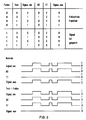
- FIG. 1 shows the inclusion of a shutdown logic AL in the electronic data processing system of an automation system AS, at the signal input SE of which one or more signals S are present.
- the signals S have a controlling effect on a processor P or other corresponding functional units of the redundant, fail-safe automation system AS, of which only one of the redundant parts is shown here.
- the signal S if it is faulty, e.g. B. too fast pulsing or so-called freezing of the signal level, significantly disrupt the program flow in the processor P. However, if the signal S is monitored in a monitoring circuit ÜW and blocked when an error is detected, the fail-safe function of the automation system AS in particular remains fully intact.
- the shutdown logic AL is controlled by two inputs.
- the error input FE activates the blocking of the signals through the shutdown logic AL.
- the test input TE brings the shutdown logic AL into the test mode. If only error input FE is activated, signal S is blocked. If the test input TE is activated, an error is additionally simulated, but the signal S is not blocked.
- test input TE and the error input FE are connected to the inputs of two NOR gates G1 and G2, the outputs of which are each connected to an input of an operating gate BT and a test gate TT.
- the signal S can also be switched through to the output by the two gates BT, TT, which are designed as AND gates.
- error signal 0
- the signal S is switched to the output A by the operating gate BT and an exclusive-OR gate G3, but the test gate TT blocks the signal.
- the duration of the test phase is to be dimensioned such that at least one signal change of the signal S takes place, because only then is the blocking function to be tested.
- the tests can be initiated by software or by a hardware timer.
- the signal level of the output signal at output A in the blocked state should be such that the subsequent functional units show no reaction.
Landscapes
- Engineering & Computer Science (AREA)
- Theoretical Computer Science (AREA)
- Quality & Reliability (AREA)
- Physics & Mathematics (AREA)
- General Engineering & Computer Science (AREA)
- General Physics & Mathematics (AREA)
- Hardware Redundancy (AREA)
- Alarm Systems (AREA)
- Debugging And Monitoring (AREA)
- Test And Diagnosis Of Digital Computers (AREA)
- Tests Of Electronic Circuits (AREA)
Claims (3)
- Dispositif de contrôle d'une installation électronique de traitement de données, qui
- lorsqu'apparaît un signal (S) erroné à l'entrée (SE) de signal de l'installation électronique de traitement de données, bloque le signal (S) au moyen d'une logique (AL) de coupure,
caractérisé en ce que le signal (S) à bloquer est appliqué à l'entrée (SE) de signal de la logique (AL) de coupure, à l'entrée (FE) d'erreur de laquelle est appliqué le signal de sortie d'un circuit (ÜW) de contrôle, qui contrôle le signal (S) à bloquer, et à l'entrée (TE) de test de laquelle est appliqué un signal de test, qui sert à tester la fonction de blocage pendant un mode test,- un signal ("1") d'erreur à l'entrée (FE) d'erreur provoquant le blocage du signal (S) à l'entrée (SE) de signal et- un signal ("1") de test à l'entrée (TE) de test et un signal ("1") d'erreur à l'entrée (FE) d'erreur ne provoquant pas le blocage du signal (S) à l'entrée (SE) de signal. - Dispositif suivant la revendication 1, caractérisé en ce que
- la logique (AL) de coupure comporte les éléments suivants :- une première porte NON-OU (G1), aux deux entrées de laquelle sont appliqués respectivement le signal d'erreur et le signal de test,- une deuxième porte NON-OU (G2), à la première entrée de laquelle est appliqué le signal d'erreur et à la deuxième entrée de laquelle est appliqué le signal de test sous forme inversée,- une première porte ET (BT), à la première entrée de laquelle est appliqué le signal de sortie inversé de la première porte NON-OU (G1) et à la deuxième entrée de laquelle est appliqué le signal à bloquer,- une deuxième porte ET (TT), à la première entrée de laquelle est appliquée la sortie de la deuxième porte NON-OU (G2) et à la deuxième entrée de laquelle est appliqué le signal à bloquer, et- une porte OU-EXCLUSIF (G3), aux entrées de laquelle sont appliquées les sorties des deux portes ET (BT, TT). - Dispositif suivant la revendication 1 ou 2, caractérisé en ce que dans un dispositif redondant comportant deux dispositifs de traitement de données, il est prévu une logique (AL) de coupure pour chaque dispositif de traitement de données.
Applications Claiming Priority (2)
| Application Number | Priority Date | Filing Date | Title |
|---|---|---|---|
| DE3821228 | 1988-06-23 | ||
| DE3821228A DE3821228A1 (de) | 1988-06-23 | 1988-06-23 | Anordnung zur ueberwachung einer elektronischen datenverarbeitungsanlage |
Publications (3)
| Publication Number | Publication Date |
|---|---|
| EP0347659A2 EP0347659A2 (fr) | 1989-12-27 |
| EP0347659A3 EP0347659A3 (fr) | 1991-03-27 |
| EP0347659B1 true EP0347659B1 (fr) | 1994-11-17 |
Family
ID=6357102
Family Applications (1)
| Application Number | Title | Priority Date | Filing Date |
|---|---|---|---|
| EP89110419A Expired - Lifetime EP0347659B1 (fr) | 1988-06-23 | 1989-06-08 | Agencement de surveillance pour une installation de traitement de données électronique |
Country Status (3)
| Country | Link |
|---|---|
| EP (1) | EP0347659B1 (fr) |
| AT (1) | ATE114197T1 (fr) |
| DE (2) | DE3821228A1 (fr) |
Families Citing this family (2)
| Publication number | Priority date | Publication date | Assignee | Title |
|---|---|---|---|---|
| US5448684A (en) * | 1993-11-12 | 1995-09-05 | Motorola, Inc. | Neural network, neuron, and method for recognizing a missing input valve |
| DE29919388U1 (de) | 1999-11-04 | 2000-04-20 | Siemens AG, 80333 München | Fehlersichere, testbare Leseschaltung für binäre Signale |
Family Cites Families (1)
| Publication number | Priority date | Publication date | Assignee | Title |
|---|---|---|---|---|
| US3479650A (en) * | 1966-06-30 | 1969-11-18 | Rca Corp | Memory driver monitoring circuit |
-
1988
- 1988-06-23 DE DE3821228A patent/DE3821228A1/de not_active Withdrawn
-
1989
- 1989-06-08 DE DE58908642T patent/DE58908642D1/de not_active Expired - Fee Related
- 1989-06-08 AT AT89110419T patent/ATE114197T1/de not_active IP Right Cessation
- 1989-06-08 EP EP89110419A patent/EP0347659B1/fr not_active Expired - Lifetime
Also Published As
| Publication number | Publication date |
|---|---|
| DE58908642D1 (de) | 1994-12-22 |
| EP0347659A2 (fr) | 1989-12-27 |
| DE3821228A1 (de) | 1989-12-28 |
| EP0347659A3 (fr) | 1991-03-27 |
| ATE114197T1 (de) | 1994-12-15 |
Similar Documents
| Publication | Publication Date | Title |
|---|---|---|
| DE3688265T2 (de) | Digitales automatisches flugsteuersystem mit ueberwachung ungleichartiger funktionen. | |
| DE69431374T2 (de) | Logischer Schaltkreis mit Fehlernachweisfunktion | |
| EP0742502A2 (fr) | Dispositif de vérification d'une valeur réelle par rapport aux valeurs d'une fenêtre de tolérance | |
| EP1873915B1 (fr) | Circuit d'entrée sécurisé doté d'un raccordement périphérique sur un canal unique pour l'entrée d'un utilisateur de bus | |
| DE4132139C2 (de) | Mikrocomputer mit Überwachungszeitgeber | |
| DE3600092C2 (fr) | ||
| CH654425A5 (en) | Redundant control arrangement | |
| DE4446314A1 (de) | Verfahren und Schaltungsanordnung zur Überwachung der Funktion einer programmgesteuerten Schaltung | |
| DE2651314C2 (de) | Sicherheits-Ausgabeschaltung für eine Binärsignale abgebende Datenverarbeitungsanlage | |
| DE19847986C2 (de) | Einzelprozessorsystem | |
| EP0347659B1 (fr) | Agencement de surveillance pour une installation de traitement de données électronique | |
| DE3938735A1 (de) | Einrichtung und verfahren zur ueberwachung einer navigationsanlage | |
| DE3938501A1 (de) | Verfahren zum betrieb eines mehrkanaligen failsafe-rechnersystems und einrichtung zur durchfuehrung des verfahrens | |
| EP1807760B1 (fr) | Systeme de traitement de donnees a frequence d'horloge variable | |
| DE10303654A1 (de) | Integrierte Halbleiterschaltung mit eingebauter Selbsttestfunktion und zugehöriges System | |
| DE4013431C2 (fr) | ||
| EP0108284B1 (fr) | Alimentation en courant d'horloge pour un système à plusieurs microcalculateurs dans des équipements de sécurité pour chemins de fer | |
| WO2002037680A1 (fr) | Appareil de commutation de securite electronique | |
| DE2949827A1 (de) | Fehler-ruecksetz-einrichtung fuer mikrocomputer | |
| DE19805518B4 (de) | Verfahren und Vorrichtung zur Analyse von Schutzsignalen für eine Anzahl von sicherheitsrelevanten Anlagenteilen einer technischen Anlage | |
| DE3644248C2 (fr) | ||
| DE4303048A1 (en) | Alarm recognition apparatus for redundant layout circuit in radio equipment - has input circuits delaying alarm recognition signals when circuits are switched to be operational systems | |
| DE4100751A1 (de) | Porterweiterungsanordnung | |
| EP1291746A2 (fr) | Circuit de sécurité électronique | |
| DD278435B5 (de) | Schaltungsanordnung zur signaltechnisch sicheren Ausgabe von Prozessdaten |
Legal Events
| Date | Code | Title | Description |
|---|---|---|---|
| PUAI | Public reference made under article 153(3) epc to a published international application that has entered the european phase |
Free format text: ORIGINAL CODE: 0009012 |
|
| AK | Designated contracting states |
Kind code of ref document: A2 Designated state(s): AT BE DE FR GB NL |
|
| 17P | Request for examination filed |
Effective date: 19901205 |
|
| PUAL | Search report despatched |
Free format text: ORIGINAL CODE: 0009013 |
|
| AK | Designated contracting states |
Kind code of ref document: A3 Designated state(s): AT BE DE FR GB NL |
|
| 17Q | First examination report despatched |
Effective date: 19940316 |
|
| GRAA | (expected) grant |
Free format text: ORIGINAL CODE: 0009210 |
|
| AK | Designated contracting states |
Kind code of ref document: B1 Designated state(s): AT BE DE FR GB NL |
|
| REF | Corresponds to: |
Ref document number: 114197 Country of ref document: AT Date of ref document: 19941215 Kind code of ref document: T |
|
| REF | Corresponds to: |
Ref document number: 58908642 Country of ref document: DE Date of ref document: 19941222 |
|
| GBT | Gb: translation of ep patent filed (gb section 77(6)(a)/1977) |
Effective date: 19950110 |
|
| ET | Fr: translation filed | ||
| PLBE | No opposition filed within time limit |
Free format text: ORIGINAL CODE: 0009261 |
|
| STAA | Information on the status of an ep patent application or granted ep patent |
Free format text: STATUS: NO OPPOSITION FILED WITHIN TIME LIMIT |
|
| 26N | No opposition filed | ||
| REG | Reference to a national code |
Ref country code: GB Ref legal event code: IF02 |
|
| PGFP | Annual fee paid to national office [announced via postgrant information from national office to epo] |
Ref country code: AT Payment date: 20020529 Year of fee payment: 14 |
|
| PGFP | Annual fee paid to national office [announced via postgrant information from national office to epo] |
Ref country code: GB Payment date: 20020610 Year of fee payment: 14 |
|
| PGFP | Annual fee paid to national office [announced via postgrant information from national office to epo] |
Ref country code: NL Payment date: 20020620 Year of fee payment: 14 |
|
| PGFP | Annual fee paid to national office [announced via postgrant information from national office to epo] |
Ref country code: FR Payment date: 20020625 Year of fee payment: 14 Ref country code: BE Payment date: 20020625 Year of fee payment: 14 |
|
| PGFP | Annual fee paid to national office [announced via postgrant information from national office to epo] |
Ref country code: DE Payment date: 20020819 Year of fee payment: 14 |
|
| PG25 | Lapsed in a contracting state [announced via postgrant information from national office to epo] |
Ref country code: GB Free format text: LAPSE BECAUSE OF NON-PAYMENT OF DUE FEES Effective date: 20030608 Ref country code: AT Free format text: LAPSE BECAUSE OF NON-PAYMENT OF DUE FEES Effective date: 20030608 |
|
| PG25 | Lapsed in a contracting state [announced via postgrant information from national office to epo] |
Ref country code: BE Free format text: LAPSE BECAUSE OF NON-PAYMENT OF DUE FEES Effective date: 20030630 |
|
| BERE | Be: lapsed |
Owner name: *SIEMENS A.G. Effective date: 20030630 |
|
| PG25 | Lapsed in a contracting state [announced via postgrant information from national office to epo] |
Ref country code: NL Free format text: LAPSE BECAUSE OF NON-PAYMENT OF DUE FEES Effective date: 20040101 Ref country code: DE Free format text: LAPSE BECAUSE OF NON-PAYMENT OF DUE FEES Effective date: 20040101 |
|
| GBPC | Gb: european patent ceased through non-payment of renewal fee |
Effective date: 20030608 |
|
| PG25 | Lapsed in a contracting state [announced via postgrant information from national office to epo] |
Ref country code: FR Free format text: LAPSE BECAUSE OF NON-PAYMENT OF DUE FEES Effective date: 20040227 |
|
| NLV4 | Nl: lapsed or anulled due to non-payment of the annual fee |
Effective date: 20040101 |
|
| REG | Reference to a national code |
Ref country code: FR Ref legal event code: ST |