EP0347659B1 - Monitoring arrangement for an electronic data processing facility - Google Patents
Monitoring arrangement for an electronic data processing facility Download PDFInfo
- Publication number
- EP0347659B1 EP0347659B1 EP89110419A EP89110419A EP0347659B1 EP 0347659 B1 EP0347659 B1 EP 0347659B1 EP 89110419 A EP89110419 A EP 89110419A EP 89110419 A EP89110419 A EP 89110419A EP 0347659 B1 EP0347659 B1 EP 0347659B1
- Authority
- EP
- European Patent Office
- Prior art keywords
- signal
- input
- data processing
- test
- gate
- Prior art date
- Legal status (The legal status is an assumption and is not a legal conclusion. Google has not performed a legal analysis and makes no representation as to the accuracy of the status listed.)
- Expired - Lifetime
Links
Images

Classifications
-
- G—PHYSICS
- G06—COMPUTING OR CALCULATING; COUNTING
- G06F—ELECTRIC DIGITAL DATA PROCESSING
- G06F11/00—Error detection; Error correction; Monitoring
- G06F11/004—Error avoidance
Definitions
- the invention relates to an arrangement for monitoring an electronic data processing system, which blocks the signal when a faulty signal occurs at the signal input of the electronic data processing system.
- control program controls the reaction of the data processing system and, in the event of a detected error, blocks the target modules on which the signal acts.
- the invention has for its object to provide an arrangement that enables control and ineffectiveness of faulty signals with circuitry means.
- the invention has the features specified in claim 1.
- An arrangement according to the preamble of claim 1 is disclosed in JP-A-59 108 163.
- Advantageous embodiments of the invention are specified in the subclaims.
- a circuit is implemented as a shutdown logic which, in conjunction with the possibly redundant structure of the data processing system, guarantees the blocking of the faulty signals. This guarantee can be achieved by making the lockability testable by means of this switch-off logic, the test not being able to interrupt the signals briefly in the fault-free case.
- the shutdown logic may be present in every redundancy. A hidden fault that is recognized during the test must also be recognized and displayed by the other redundancies.
- FIG. 1 shows the inclusion of a shutdown logic AL in the electronic data processing system of an automation system AS, at the signal input SE of which one or more signals S are present.
- the signals S have a controlling effect on a processor P or other corresponding functional units of the redundant, fail-safe automation system AS, of which only one of the redundant parts is shown here.
- the signal S if it is faulty, e.g. B. too fast pulsing or so-called freezing of the signal level, significantly disrupt the program flow in the processor P. However, if the signal S is monitored in a monitoring circuit ÜW and blocked when an error is detected, the fail-safe function of the automation system AS in particular remains fully intact.
- the shutdown logic AL is controlled by two inputs.
- the error input FE activates the blocking of the signals through the shutdown logic AL.
- the test input TE brings the shutdown logic AL into the test mode. If only error input FE is activated, signal S is blocked. If the test input TE is activated, an error is additionally simulated, but the signal S is not blocked.
- test input TE and the error input FE are connected to the inputs of two NOR gates G1 and G2, the outputs of which are each connected to an input of an operating gate BT and a test gate TT.
- the signal S can also be switched through to the output by the two gates BT, TT, which are designed as AND gates.
- error signal 0
- the signal S is switched to the output A by the operating gate BT and an exclusive-OR gate G3, but the test gate TT blocks the signal.
- the duration of the test phase is to be dimensioned such that at least one signal change of the signal S takes place, because only then is the blocking function to be tested.
- the tests can be initiated by software or by a hardware timer.
- the signal level of the output signal at output A in the blocked state should be such that the subsequent functional units show no reaction.
Landscapes
- Engineering & Computer Science (AREA)
- Theoretical Computer Science (AREA)
- Quality & Reliability (AREA)
- Physics & Mathematics (AREA)
- General Engineering & Computer Science (AREA)
- General Physics & Mathematics (AREA)
- Hardware Redundancy (AREA)
- Alarm Systems (AREA)
- Debugging And Monitoring (AREA)
- Tests Of Electronic Circuits (AREA)
- Test And Diagnosis Of Digital Computers (AREA)
Abstract
Description
Die Erfindung betrifft eine Anordnung zur Überwachung einer elektronischen Datenverarbeitungsanlage, die bei Auftreten eines fehlerhaften Signals am Signaleingang der elektronischen Datenverarbeitungsanlage das Signal sperrt.The invention relates to an arrangement for monitoring an electronic data processing system, which blocks the signal when a faulty signal occurs at the signal input of the electronic data processing system.
Es ist bekannt, mit entsprechenden Kontrollprogrammen in Datenverarbeitungsanlagen fehlerhafte Eingangssignale, die den eigentlichen Programmablauf stören, dadurch zu erkennen, daß das Kontrollprogramm die Reaktion der Datenverarbeitungsanlage kontrolliert und bei einem festgestellten Fehler die Zielbausteine, auf die das Signal wirkt, sperrt.It is known, with appropriate control programs in data processing systems, to recognize faulty input signals which interfere with the actual program flow, in that the control program controls the reaction of the data processing system and, in the event of a detected error, blocks the target modules on which the signal acts.
Der Erfindung liegt die Aufgabe zugrunde, eine Anordnung zu schaffen, die mit schaltungstechnischen Mitteln eine Kontrolle und Unwirksammachung von fehlerhaften Signalen ermöglicht.The invention has for its object to provide an arrangement that enables control and ineffectiveness of faulty signals with circuitry means.
Zur Lösung dieser Aufgabe weist die Erfindung die in Anspruch 1 angegebenen Merkmale auf. Eine Anordnung gemäß dem Oberbegriff des Anspruchs 1 ist aus der Patentschnift JP-A- 59 108 163 bekannt gegeben. Vorteilhafte Ausgestaltungen der Erfindung sind in den Unteransprüchen angegeben.To achieve this object, the invention has the features specified in
Die erfindungsgemäße Lösung ist vor allem in vorteilhafter Weise bei redundanten, fehlersicheren Automatisierungssystemen anwendbar. Bei solchen Systemen ist es erforderlich, daß Signale, die von außen zeitlich willkürlich ins System gebracht werden, z. B. Prozeßinterrupts, im Fehlerfall gesperrt werden müssen, um so das System zu schützen und keine falschen oder unnötigen Reaktionen oder gar Programmblockierungen hervorzurufen.The solution according to the invention can above all be used advantageously in redundant, fail-safe automation systems. In such systems, it is necessary that signals that are arbitrarily brought into the system from the outside, e.g. B. process interrupts must be blocked in the event of an error, so as to protect the system and no wrong or cause unnecessary reactions or even program blocks.
Gemäß der Erfindung ist eine Schaltung als Abschaltlogik realisiert, die, im Verbund mit dem eventuell redundanten Aufbau der Datenverarbeitungsanlage, das Sperren der fehlerhaften Signale garantiert. Diese Garantie kann man dadurch erreichen, daß man das Sperrenkönnen durch diese Abschaltlogik testbar macht, wobei der Test die Signale im fehlerfreien Fall auch nicht nur kurzzeitig unterbrechen darf. Die Abschaltlogik ist dabei gegebenenfalls in jeder Redundanz vorhanden. Einen verdeckten Fehler, der beim Test erkannt wird, müssen hierbei auch die jeweils anderen Redundanzen erkennen und anzeigen.According to the invention, a circuit is implemented as a shutdown logic which, in conjunction with the possibly redundant structure of the data processing system, guarantees the blocking of the faulty signals. This guarantee can be achieved by making the lockability testable by means of this switch-off logic, the test not being able to interrupt the signals briefly in the fault-free case. The shutdown logic may be present in every redundancy. A hidden fault that is recognized during the test must also be recognized and displayed by the other redundancies.
- Figur 1Figure 1
- zeigt den prinzipiellen Aufbau eines Automatisierungssystems mit Abschaltlogik,shows the basic structure of an automation system with shutdown logic,
- Figur 2Figure 2
- ein Detailschaltbild der Abschaltlogik unda detailed circuit diagram of the shutdown logic and
- Figur 3Figure 3
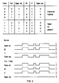
- eine Wertetabelle mit Zeitdiagrammen der Signale in der Abschaltlogik.a table of values with time diagrams of the signals in the shutdown logic.
In der Figur 1 ist die Einbeziehung einer Abschaltlogik AL in die elektronische Datenverarbeitungsanlage eines Automatisierungssystems AS ersichtlich, an deren Signaleingang SE ein oder mehrere Signale S anliegen. Die Signale S wirken steuernd auf einen Prozessor P oder andere entsprechende Funktionseinheiten des redundanten, fehlersicheren Automatisierungssystems AS, von dem hier nur einer der redundant ausgeführten Teile dargestellt ist. Das Signal S kann, wenn es fehlerhaft ist, z. B. zu schnelles Pulsen oder sogenanntes Einfrieren des Signalpegels, den Programmablauf im Prozessor P erheblich stören. Wird das Signal S jedoch in einer Überwachungsschaltung ÜW überwacht und bei einem erkannten Fehler gesperrt, bleibt insbesondere die fehlersichere Funktion des Automatisierungssystems AS voll erhalten. Die Abschaltlogik AL wird von zwei Eingängen gesteuert. Der Fehlereingang FE aktiviert das Sperren der Signale durch die Abschaltlogik AL. Der Testeingang TE bringt die Abschaltlogik AL in den Testmodus. Wird nur der Fehlereingang FE angesteuert, wird das Signal S gesperrt. Wird der Testeingang TE angesteuert, wird ein Fehler zusätzlich simuliert, das Signal S jedoch nicht gesperrt.FIG. 1 shows the inclusion of a shutdown logic AL in the electronic data processing system of an automation system AS, at the signal input SE of which one or more signals S are present. The signals S have a controlling effect on a processor P or other corresponding functional units of the redundant, fail-safe automation system AS, of which only one of the redundant parts is shown here. The signal S, if it is faulty, e.g. B. too fast pulsing or so-called freezing of the signal level, significantly disrupt the program flow in the processor P. However, if the signal S is monitored in a monitoring circuit ÜW and blocked when an error is detected, the fail-safe function of the automation system AS in particular remains fully intact. The shutdown logic AL is controlled by two inputs. The error input FE activates the blocking of the signals through the shutdown logic AL. The test input TE brings the shutdown logic AL into the test mode. If only error input FE is activated, signal S is blocked. If the test input TE is activated, an error is additionally simulated, but the signal S is not blocked.
Die detaillierte Funktion der Abschaltlogik AL soll anhand der Figuren 2 und 3 erläutert werden.The detailed function of the shutdown logic AL will be explained with reference to FIGS. 2 and 3.
Der Testeingang TE und der Fehlereingang FE sind auf die Eingänge von zwei NOR-Gattern G1 und G2 geführt, deren Ausgänge jeweils mit einem Eingang eines Betriebstores BT und eines Testtores TT verbunden sind. Das Signal S kann ebenfalls durch die zwei Tore BT, TT an den Ausgang durchgeschaltet werden, die als AND-Gatter ausgeführt sind. Im fehlerfreien Fall (Fehlersignal = 0) wird das Signal S durch das Betriebstor BT und ein Exklusiv-ODER-Gatter G3 an den Ausgang A geschaltet, das Testtor TT dagegen sperrt das Signal. Im Testbetrieb (Testsignal = 1) sperrt das Betriebstor BT das Signal S, und das Testtor TT läßt das Signal S durch, wie es auch aus der Wertetabelle gemäß Figur 3 ersichtlich ist. Im Testmodus wird somit das Signal S nicht gesperrt. Kann eines der beiden Tore BT oder TT nicht mehr sperren, so liegt das Signal S an beiden Eingängen des Exklusiv-ODER-Gatters G3, so daß sich eine statische Null am Ausgang A einstellt. Wenn beide Tore BT, TT durch einen Fehler gesperrt werden, ergibt sich ebenfalls auch eine statische Null am Ausgang A. Da ein Signalwechsel am Signaleingang des Prozessors P eine bestimmte Reaktion hervorruft, führt ein statisch anliegendes Signal S natürlich zu einer Abweichung der Programmbearbeitung des Prozessors P in der Redundanz mit der defekten Abschaltlogik AL. Die Software der elektronischen Datenverarbeitungsanlage erkennt diese Asynchronität jedoch auf einfache Weise (u. U. unterstützt durch einen Hardware-Vergleicher) und veranlaßt eine entsprechende Fehlermeldung.The test input TE and the error input FE are connected to the inputs of two NOR gates G1 and G2, the outputs of which are each connected to an input of an operating gate BT and a test gate TT. The signal S can also be switched through to the output by the two gates BT, TT, which are designed as AND gates. In the error-free case (error signal = 0), the signal S is switched to the output A by the operating gate BT and an exclusive-OR gate G3, but the test gate TT blocks the signal. In test mode (test signal = 1), the operating gate BT blocks the signal S, and the test gate TT lets the signal S pass, as can also be seen from the table of values in FIG. 3. The signal S is thus not blocked in the test mode. If one of the two gates BT or TT can no longer block, then the signal S is present at both inputs of the exclusive OR gate G3, so that a static zero is set at the output A. If both gates BT, TT are blocked by an error, there is also a static zero at output A. Since a signal change at the signal input of processor P causes a certain reaction, a statically applied signal S naturally leads to a deviation in the program processing of the processor P in redundancy with the defective shutdown logic AL. The software of the electronic data processing system recognizes this asynchrony in a simple manner (possibly supported by a hardware comparator) and triggers a corresponding error message.
Die Dauer der Testphase ist so zu bemessen, daß mindestens ein Signalwechsel des Signals S stattfindet, weil dann erst die Sperrfunktion zu testen ist. Die Tests können per Software oder durch einen Hardware-Timer angestoßen werden. Der Signalpegel des Ausgangssignals am Ausgang A im gesperrten Zustand sollte so sein, daß die nachfolgenden Funktionseinheiten keine Reaktion zeigen.The duration of the test phase is to be dimensioned such that at least one signal change of the signal S takes place, because only then is the blocking function to be tested. The tests can be initiated by software or by a hardware timer. The signal level of the output signal at output A in the blocked state should be such that the subsequent functional units show no reaction.
Claims (3)
- An arrangement for monitoring an electronic data processing installation which
- on the occurrence of a faulty signal (S) at the signal input (SE) of the electronic data processing installation blocks the signal (S) by means of a deactivating logic circuit (AL),
characterised in that the signal (S) to be blocked occurs at the signal input (SE) of the deactivating logic circuit (AL), the output signal of a monitoring circuit (ÜW) occurs at the fault input (FE) of said deactivating logic circuit, and a test signal, which in a test mode serves to test the blocking function, occurs at the test input (TE) of said deactivating logic circuit, where- a fault signal ("1") at the fault input (FE) leads to the blockage of the signal (S) at the signal input (SE) and- a test signal ("1") at the test input (TE) and a fault signal ("1") at the fault input (FE) does not lead to the blockage of the signal (S) at the signal input (SE). - An arrangement as claimed in Claim 1, characterised in that- the deactivating logic circuit (AL) comprises the following elements:- a first NOR-gate (G1), at the two inputs of which the fault signal and the test signal respectively occur,- a second NOR-gate (G2), at the first input of which the fault signal occurs and at the second input of which the test signal occurs in negated form,- a first AND-gate (BT), at the first input of which the negated output signal of the first NOR-gate (G1) and at the second input of which the signal to be blocked occur,- a second AND-gate (TT), to the first input of which the output of the second NOR gate (G2) is connected and at the second input of which the signal to be blocked occurs and- an exclusive-OR-gate (G3), the inputs of which are connected to the outputs of the two AND-gates (BT, TT).
- An arrangement as claimed in Claim 1 or Claim 2, characterised in that
- in the case of a redundant arrangement comprising two electronic data processing installations a respective deactivating logic circuit (AL) is provided for each data processing installation.
Applications Claiming Priority (2)
| Application Number | Priority Date | Filing Date | Title |
|---|---|---|---|
| DE3821228 | 1988-06-23 | ||
| DE3821228A DE3821228A1 (en) | 1988-06-23 | 1988-06-23 | ARRANGEMENT FOR MONITORING AN ELECTRONIC DATA PROCESSING SYSTEM |
Publications (3)
| Publication Number | Publication Date |
|---|---|
| EP0347659A2 EP0347659A2 (en) | 1989-12-27 |
| EP0347659A3 EP0347659A3 (en) | 1991-03-27 |
| EP0347659B1 true EP0347659B1 (en) | 1994-11-17 |
Family
ID=6357102
Family Applications (1)
| Application Number | Title | Priority Date | Filing Date |
|---|---|---|---|
| EP89110419A Expired - Lifetime EP0347659B1 (en) | 1988-06-23 | 1989-06-08 | Monitoring arrangement for an electronic data processing facility |
Country Status (3)
| Country | Link |
|---|---|
| EP (1) | EP0347659B1 (en) |
| AT (1) | ATE114197T1 (en) |
| DE (2) | DE3821228A1 (en) |
Families Citing this family (2)
| Publication number | Priority date | Publication date | Assignee | Title |
|---|---|---|---|---|
| US5448684A (en) * | 1993-11-12 | 1995-09-05 | Motorola, Inc. | Neural network, neuron, and method for recognizing a missing input valve |
| DE29919388U1 (en) | 1999-11-04 | 2000-04-20 | Siemens AG, 80333 München | Fail-safe, testable reading circuit for binary signals |
Family Cites Families (1)
| Publication number | Priority date | Publication date | Assignee | Title |
|---|---|---|---|---|
| US3479650A (en) * | 1966-06-30 | 1969-11-18 | Rca Corp | Memory driver monitoring circuit |
-
1988
- 1988-06-23 DE DE3821228A patent/DE3821228A1/en not_active Withdrawn
-
1989
- 1989-06-08 AT AT89110419T patent/ATE114197T1/en not_active IP Right Cessation
- 1989-06-08 DE DE58908642T patent/DE58908642D1/en not_active Expired - Fee Related
- 1989-06-08 EP EP89110419A patent/EP0347659B1/en not_active Expired - Lifetime
Also Published As
| Publication number | Publication date |
|---|---|
| DE58908642D1 (en) | 1994-12-22 |
| EP0347659A3 (en) | 1991-03-27 |
| DE3821228A1 (en) | 1989-12-28 |
| EP0347659A2 (en) | 1989-12-27 |
| ATE114197T1 (en) | 1994-12-15 |
Similar Documents
| Publication | Publication Date | Title |
|---|---|---|
| DE3688265T2 (en) | DIGITAL AUTOMATIC FLIGHT CONTROL SYSTEM WITH MONITORING OF UNIQUE FUNCTIONS. | |
| DE69431374T2 (en) | Logical circuit with error detection function | |
| EP0742502A2 (en) | Device for checking an actual value in relation to values of a tolerance window | |
| EP1873915B1 (en) | Secure input circuit with single channel peripheral connection for the input of a bus participant | |
| DE4132139C2 (en) | Microcomputer with watchdog timer | |
| DE3600092C2 (en) | ||
| CH654425A5 (en) | Redundant control arrangement | |
| DE4446314A1 (en) | Method and circuit arrangement for monitoring the function of a program-controlled circuit | |
| DE2651314C2 (en) | Safety output circuit for a data processing system that emits binary signals | |
| DE19847986C2 (en) | Single processor system | |
| EP0347659B1 (en) | Monitoring arrangement for an electronic data processing facility | |
| DE19622639B4 (en) | Wafer stepper with one interface | |
| DE3938735A1 (en) | DEVICE AND METHOD FOR MONITORING A NAVIGATION SYSTEM | |
| DE3938501A1 (en) | METHOD FOR OPERATING A MULTI-CHANNEL FAILSAFE COMPUTER SYSTEM AND DEVICE FOR IMPLEMENTING THE METHOD | |
| EP1807760B1 (en) | Data processing system with a variable clock speed | |
| DE10303654A1 (en) | Integrated semiconductor circuit with built-in self-test function and associated system | |
| EP0108284B1 (en) | Clock current supply for a multimicrocomputer system in railways safety equipments | |
| WO2002037680A1 (en) | Electronic safety switching device | |
| DE19857396C2 (en) | Fail-safe binary comparator with ternary result and status display | |
| DE2949827A1 (en) | Error reset for microprocessor - has error reset unit generating control signals automatically setting digital control unit to basic mode operation | |
| DE19805518B4 (en) | Method and device for analyzing protection signals for a number of safety-relevant plant parts of a technical installation | |
| DE3644248C2 (en) | ||
| DE4303048A1 (en) | Alarm recognition apparatus for redundant layout circuit in radio equipment - has input circuits delaying alarm recognition signals when circuits are switched to be operational systems | |
| DE4100751A1 (en) | Port expansion unit for engine management controller - includes comparator units coupled to interrupt generator to indicate faults in load circuits | |
| EP1291746A2 (en) | Electronic safety circuit |
Legal Events
| Date | Code | Title | Description |
|---|---|---|---|
| PUAI | Public reference made under article 153(3) epc to a published international application that has entered the european phase |
Free format text: ORIGINAL CODE: 0009012 |
|
| AK | Designated contracting states |
Kind code of ref document: A2 Designated state(s): AT BE DE FR GB NL |
|
| 17P | Request for examination filed |
Effective date: 19901205 |
|
| PUAL | Search report despatched |
Free format text: ORIGINAL CODE: 0009013 |
|
| AK | Designated contracting states |
Kind code of ref document: A3 Designated state(s): AT BE DE FR GB NL |
|
| 17Q | First examination report despatched |
Effective date: 19940316 |
|
| GRAA | (expected) grant |
Free format text: ORIGINAL CODE: 0009210 |
|
| AK | Designated contracting states |
Kind code of ref document: B1 Designated state(s): AT BE DE FR GB NL |
|
| REF | Corresponds to: |
Ref document number: 114197 Country of ref document: AT Date of ref document: 19941215 Kind code of ref document: T |
|
| REF | Corresponds to: |
Ref document number: 58908642 Country of ref document: DE Date of ref document: 19941222 |
|
| GBT | Gb: translation of ep patent filed (gb section 77(6)(a)/1977) |
Effective date: 19950110 |
|
| ET | Fr: translation filed | ||
| PLBE | No opposition filed within time limit |
Free format text: ORIGINAL CODE: 0009261 |
|
| STAA | Information on the status of an ep patent application or granted ep patent |
Free format text: STATUS: NO OPPOSITION FILED WITHIN TIME LIMIT |
|
| 26N | No opposition filed | ||
| REG | Reference to a national code |
Ref country code: GB Ref legal event code: IF02 |
|
| PGFP | Annual fee paid to national office [announced via postgrant information from national office to epo] |
Ref country code: AT Payment date: 20020529 Year of fee payment: 14 |
|
| PGFP | Annual fee paid to national office [announced via postgrant information from national office to epo] |
Ref country code: GB Payment date: 20020610 Year of fee payment: 14 |
|
| PGFP | Annual fee paid to national office [announced via postgrant information from national office to epo] |
Ref country code: NL Payment date: 20020620 Year of fee payment: 14 |
|
| PGFP | Annual fee paid to national office [announced via postgrant information from national office to epo] |
Ref country code: FR Payment date: 20020625 Year of fee payment: 14 Ref country code: BE Payment date: 20020625 Year of fee payment: 14 |
|
| PGFP | Annual fee paid to national office [announced via postgrant information from national office to epo] |
Ref country code: DE Payment date: 20020819 Year of fee payment: 14 |
|
| PG25 | Lapsed in a contracting state [announced via postgrant information from national office to epo] |
Ref country code: GB Free format text: LAPSE BECAUSE OF NON-PAYMENT OF DUE FEES Effective date: 20030608 Ref country code: AT Free format text: LAPSE BECAUSE OF NON-PAYMENT OF DUE FEES Effective date: 20030608 |
|
| PG25 | Lapsed in a contracting state [announced via postgrant information from national office to epo] |
Ref country code: BE Free format text: LAPSE BECAUSE OF NON-PAYMENT OF DUE FEES Effective date: 20030630 |
|
| BERE | Be: lapsed |
Owner name: *SIEMENS A.G. Effective date: 20030630 |
|
| PG25 | Lapsed in a contracting state [announced via postgrant information from national office to epo] |
Ref country code: NL Free format text: LAPSE BECAUSE OF NON-PAYMENT OF DUE FEES Effective date: 20040101 Ref country code: DE Free format text: LAPSE BECAUSE OF NON-PAYMENT OF DUE FEES Effective date: 20040101 |
|
| GBPC | Gb: european patent ceased through non-payment of renewal fee |
Effective date: 20030608 |
|
| PG25 | Lapsed in a contracting state [announced via postgrant information from national office to epo] |
Ref country code: FR Free format text: LAPSE BECAUSE OF NON-PAYMENT OF DUE FEES Effective date: 20040227 |
|
| NLV4 | Nl: lapsed or anulled due to non-payment of the annual fee |
Effective date: 20040101 |
|
| REG | Reference to a national code |
Ref country code: FR Ref legal event code: ST |