EP0347322B1 - Stabilisierte Versorgung mit reduziertem Brummspannungsverhältnis - Google Patents
Stabilisierte Versorgung mit reduziertem Brummspannungsverhältnis Download PDFInfo
- Publication number
- EP0347322B1 EP0347322B1 EP89401678A EP89401678A EP0347322B1 EP 0347322 B1 EP0347322 B1 EP 0347322B1 EP 89401678 A EP89401678 A EP 89401678A EP 89401678 A EP89401678 A EP 89401678A EP 0347322 B1 EP0347322 B1 EP 0347322B1
- Authority
- EP
- European Patent Office
- Prior art keywords
- circuit
- voltage
- transformers
- power supply
- rectifier
- Prior art date
- Legal status (The legal status is an assumption and is not a legal conclusion. Google has not performed a legal analysis and makes no representation as to the accuracy of the status listed.)
- Expired - Lifetime
Links
- 230000010363 phase shift Effects 0.000 claims description 6
- 230000001960 triggered effect Effects 0.000 claims description 5
- 238000004804 winding Methods 0.000 claims description 5
- 239000003990 capacitor Substances 0.000 description 14
- 238000001914 filtration Methods 0.000 description 4
- 238000010586 diagram Methods 0.000 description 2
- 238000009434 installation Methods 0.000 description 2
- 230000035939 shock Effects 0.000 description 2
- 230000000903 blocking effect Effects 0.000 description 1
- 230000001276 controlling effect Effects 0.000 description 1
- 239000006185 dispersion Substances 0.000 description 1
- 230000000694 effects Effects 0.000 description 1
- 230000009931 harmful effect Effects 0.000 description 1
- 238000009413 insulation Methods 0.000 description 1
- 238000002955 isolation Methods 0.000 description 1
- 238000004519 manufacturing process Methods 0.000 description 1
- 244000045947 parasite Species 0.000 description 1
- 230000002688 persistence Effects 0.000 description 1
- 230000001105 regulatory effect Effects 0.000 description 1
- 230000000630 rising effect Effects 0.000 description 1
Images
Classifications
-
- H—ELECTRICITY
- H02—GENERATION; CONVERSION OR DISTRIBUTION OF ELECTRIC POWER
- H02M—APPARATUS FOR CONVERSION BETWEEN AC AND AC, BETWEEN AC AND DC, OR BETWEEN DC AND DC, AND FOR USE WITH MAINS OR SIMILAR POWER SUPPLY SYSTEMS; CONVERSION OF DC OR AC INPUT POWER INTO SURGE OUTPUT POWER; CONTROL OR REGULATION THEREOF
- H02M7/00—Conversion of AC power input into DC power output; Conversion of DC power input into AC power output
- H02M7/42—Conversion of DC power input into AC power output without possibility of reversal
- H02M7/44—Conversion of DC power input into AC power output without possibility of reversal by static converters
- H02M7/48—Conversion of DC power input into AC power output without possibility of reversal by static converters using discharge tubes with control electrode or semiconductor devices with control electrode
- H02M7/497—Conversion of DC power input into AC power output without possibility of reversal by static converters using discharge tubes with control electrode or semiconductor devices with control electrode sinusoidal output voltages being obtained by combination of several voltages being out of phase
-
- H—ELECTRICITY
- H02—GENERATION; CONVERSION OR DISTRIBUTION OF ELECTRIC POWER
- H02M—APPARATUS FOR CONVERSION BETWEEN AC AND AC, BETWEEN AC AND DC, OR BETWEEN DC AND DC, AND FOR USE WITH MAINS OR SIMILAR POWER SUPPLY SYSTEMS; CONVERSION OF DC OR AC INPUT POWER INTO SURGE OUTPUT POWER; CONTROL OR REGULATION THEREOF
- H02M3/00—Conversion of DC power input into DC power output
- H02M3/22—Conversion of DC power input into DC power output with intermediate conversion into AC
- H02M3/24—Conversion of DC power input into DC power output with intermediate conversion into AC by static converters
- H02M3/28—Conversion of DC power input into DC power output with intermediate conversion into AC by static converters using discharge tubes with control electrode or semiconductor devices with control electrode to produce the intermediate AC
- H02M3/305—Conversion of DC power input into DC power output with intermediate conversion into AC by static converters using discharge tubes with control electrode or semiconductor devices with control electrode to produce the intermediate AC using devices of a thyratron or thyristor type requiring extinguishing means
- H02M3/315—Conversion of DC power input into DC power output with intermediate conversion into AC by static converters using discharge tubes with control electrode or semiconductor devices with control electrode to produce the intermediate AC using devices of a thyratron or thyristor type requiring extinguishing means using semiconductor devices only
- H02M3/3155—Conversion of DC power input into DC power output with intermediate conversion into AC by static converters using discharge tubes with control electrode or semiconductor devices with control electrode to produce the intermediate AC using devices of a thyratron or thyristor type requiring extinguishing means using semiconductor devices only with automatic control of the output voltage or current
-
- H—ELECTRICITY
- H05—ELECTRIC TECHNIQUES NOT OTHERWISE PROVIDED FOR
- H05G—X-RAY TECHNIQUE
- H05G1/00—X-ray apparatus involving X-ray tubes; Circuits therefor
- H05G1/08—Electrical details
- H05G1/26—Measuring, controlling or protecting
- H05G1/30—Controlling
- H05G1/32—Supply voltage of the X-ray apparatus or tube
Definitions
- the subject of the present invention is a stabilized power supply with a reduced ripple rate, usable in particular in the medical field for electrically supplying X-ray tubes. It can nevertheless be applied to other fields where the need for large powers is encountered.
- electric of the order of one hundred kilowatts (KW) and at very high voltages, for example of the order of 100 kilovolts (KV). It mainly relates to voltage rise supplies, of the continuous continuous type, provided with an inverter.
- a DC-type voltage rise supply generally comprises a first rectifier connectable to an electrical distribution network.
- the rectified and filtered voltage delivered by this rectifier is introduced into a variable frequency inverter which delivers a wavy signal.
- the rippled signal is then applied to a step-up transformer, itself in connection with a second rectifier to produce a rectified high voltage.
- a rectified high voltage can for example be used to control an X-ray tube by providing the necessary potential difference between the cathode and the anode of this tube.
- the regulation of the high voltage delivered is generally obtained by varying the ripple frequency of the inverter, so as to act on its power transfer function as a function of the frequency.
- inverters in DC-type voltage rise power supplies
- the reinjection into the electrical network of reactive energy due to the switching in the inverter is simply doubled, tripled, multiplied by n, when the power thus produced doubles, triples, or is multiplied n times.
- it is necessary to place in the filter circuit of the first rectifier very important filters, therefore very bulky and very expensive. These filters then become all the more expensive as the power is increased.
- Such power supplies are for example described in document WO 86/04749. However, we find there both the industrialization problems and the switching problems mentioned.
- the object of the invention is to remedy these drawbacks by recommending a solution which, at multiple power, borrows exactly the already tried industrial solutions, including the ripple rate of the high voltage across the load, and whose energy reactive feed back into the network are significantly reduced. In practice, a reduction is obtained in a ratio 4.
- the principle of the invention is based on the use of two, three, n identical inverters connected in parallel to the output of the first rectifier, and the triggering of which is out of phase with the relative to each other, in phase quadrature, with a 2 ⁇ / 3 phase shift, with a 2 ⁇ / n phase shift. We can then show that each inverter can provide a fraction P / n of the total power P to be transmitted.
- the structure of a high-voltage block must also ensure perfect balancing between a positive and a negative channel. As it is unlikely that, despite all the precautions taken, the 2 or n inverters thus put into service have equal transfer characteristics, in an improvement we share the contribution of each of these inverters to the positive path of a on the one hand and the negative path on the other. In this improvement, the voltage elevation circuit at the output of the ripple circuit is then a little more complex in its connection to allow, with the use of already proven step-up transformers, balancing between the channels. This balancing is independent of the characteristics of the inverters, and, for each inverter when they are two-wave, between one wave and the other.
- the subject of the invention is therefore a stabilized power supply with a reduced ripple rate according to claim 1 and 2.
- the inverters are of the double-alternation type, and the phase shifts are therefore equal to ⁇ / n.
- the invention relates to a stabilized power supply with a reduced ripple rate according to claim 2.
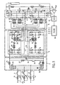
- FIG. 1 shows a stabilized power supply with a reduced ripple rate according to the invention.
- This is in particular intended to supply an X-ray tube 1 usable in a medical application.
- This supply essentially comprises a first rectifier 2 connected to an electrical network 3.
- a ripple circuit 4 makes it possible to ripple a rectified and filtered direct voltage delivered by the first rectifier 2.
- a voltage rise circuit 5 raises the voltage of the signal delivered by the ripple circuit.
- the circuit 5 is connected to a second rectifier 6 intended to produce a high direct voltage from an alternating high voltage delivered by the booster circuit 5.
- the circuit 4 comprises the inverters 7 and 8 respectively.
- these inverters 7 and 8 are of the bi-alternation type and each comprise 2 sets of switches for passing the current alternately in one direction and then in another, in a resonant circuit.
- the operation of the power supply according to the invention is as follows.
- a set of switches 9 to 11 is switched to allow connection of the rectifier 2 to the electrical network 3 by means of resistors in series respectively 12 to 14.
- resistors 12 to 14 are justified by the high power available nature of the power supply to be produced and by the concern to limit the inrush current at ignition in the electrical network.
- Resistors 12 to 14 are only used for precharging the capacitors of the downstream filter. They are only used when the converters are energized, which in turn ensure the rise of high voltage.
- Resistors 12 to 14 play, with the filtering capacities of rectifier 2, a role of low-pass circuit: the starting current does not increase too suddenly.
- the alternating signal delivered by the network 3 is thus applied to the input of a conventional rectifier 2 with diodes 18 to 23.
- the diode rectifier supplies a rectified voltage in a filter cell essentially comprising a filtering capacitor 24 and two shock inductors 25 and 26.
- the capacitor 24 is connected in series between the inductors 25 and 26, the whole is connected in parallel to the diode rectifier.
- a voltage thus rectified and filtered is then available across the capacitor 24.
- a resistor 27 in series with a switch 28 is also placed in parallel on the capacitor 24.
- the ripple circuit comprises n inverters, and in the example a preferred solution will be described with two inverters 7 and 8.
- Each inverter is connected, at its input, in parallel with the output of the first rectifier 2.
- the two inverters are similar.
- the inverter 7 comprises two sets of thyristors respectively T1 T4 and T3 T respectivement. Each set of thyristors is connected in series on either side of a resonant circuit comprising an inductor 29, a capacitor 30 and a primary winding 31 of a transformer 32.
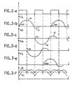
- this inverter is as follows, see Figures 2a to 2c.
- the triggers of the thyristors T1 and T4 are triggered by an order issued by a pilot circuit 33.
- the current then passes through the thyristor T1, in the inductor 29, in the capacitor 30, and in the primary of the transformer 31, to close by thyristor T4 on the output of rectifier 2.
- a positive alternation 34 then arises in the resonant circuit 29 to 31. This alternation gives rise by resonance to a negative reaction alternation 35.
- the current of the reaction alternation 35 is fed back into rectifier 2 via diodes D4 and D1 respectively in parallel on the thyristors T4 and T1.
- the diodes D1 and D4 which allow the passage of the alternation of reaction allow the blocking of the thyristors T1 and T4 until their next triggering.
- the pilot circuit 33 triggers the play of the thyristors T3 and T2 also tending to pass a charge current, but in the opposite direction , in the resonant circuit 29 to 31.
- the thyristors T3 and T2 then give rise to a negative alternation 36 which combines with the alternation 35.
- the alternation 36 gives in the same way as the alternation 34 birth to an alternation of reaction 37.
- the inverter 8 is comparable in all respects to the inverter 7 except that the triggering of its thyristors T5 T8 or T7 T6 is caused in phase quadrature, at times t ⁇ / 2 or t 3 ⁇ / 2 , with respect to at the instants at which the thyristors T1 T4 and T3 T2 are triggered. It follows that the secondary 39 of the transformer 40 of the resonant circuit of the inverter 8 delivers a signal, also sinusoidal, but phase-shifted in quadrature with respect to the signal delivered by secondary 38. We can easily generalize in the case where there are n inverters. In this case the signals delivered by these inverters would be phase-shifted by 2 ⁇ / n, or more exactly by ⁇ / n with, as here, full-wave inverters.
- the signals available on the secondary 38 and 39 are then sent in a booster circuit 5 which, according to a variant, comprises two transformers 41 and 42.
- the two primary respectively 43 and 44 of these transformers 41 and 42 are connected to the secondary, respectively 38 and 39.
- the secondaries 45 and 46 respectively of transformers 41 and 42 are in series with each other and supply a second diode rectifier circuit 47 to 50 of the same type as the first rectifier 2.
- This second rectifier is connected in parallel with two capacitors in series 51 and 52. To balance the assembly, the midpoint of the capacitors 51 and 52 is even connected to the midpoint of the secondaries 45 and 46.
- Other variants are possible.
- this combination of the signals in phase quadrature in two transformers 41, 42 with secondary in series, or in a single transformer with n primary has the effect of delivering a rectified signal with n times more peaks than if there were only one inverter.
- FIG. 2f shows comparatively the undulations 53 obtained after rectification of a signal according to the invention, and the less frequent undulations 54, but at the same time much larger when there is only one inverter.
- the reactive currents compensate each other, which further improves performance.
- the invention naturally has the advantage of using two similar inverters twice, that is to say having successfully undergone a previous industrialization test. Ultimately, the definition of a stabilized power supply with a low ripple rate but at a higher power is thus greatly facilitated.
- the inverters 7 and 8 are not strictly identical. To remedy this drawback, it is recommended to duplicate the transformers such as 41 and 42 in the booster circuit. Two other (n others) 55 and 56 are then mounted, the primaries of which are connected in parallel with the primaries of the transformers 41 and 42 and whose secondary 57 and 58 are connected in series with each other. These secondary 57 and 58 are also connected to another second rectifier circuit, identical to circuit 48-52.
- This second identical rectifier comprises in particular two capacitors in series 59 and 60 at output. We can consider that in parallel with the capacitors 51 and 52 we have the positive channel, and that in parallel with the capacitors 59 and 60 we have a negative channel. It is then possible, by connecting the capacitors 52 and 59 in series, to have a midpoint connectable to ground. In this way, the difficulties of electrical isolation in very high voltage use are reduced. In practice, the insulation constraints are then divided by 2.
- a resistance divider bridge 61 and 62 is connected, the midpoint of which is connected to a comparator 63.
- the comparator 63 also receives a reference voltage V on a comparison input. ref .
- the error signal delivered by the comparator 63 is introduced in a known manner into a voltage frequency converter 64 (VCO) which outputs a square signal, of duty cycle 1, in the pilot circuit 33.
- VCO voltage frequency converter
- FIG. 2a changes so as to keep the phase shift in quadrature of attack of the inverters 7 and 8.
- a duty cycle of 1 corresponds to a pulse signal whose pulse duration is equal to the duration during which the pulse is absent.
- the frequency of the voltage-frequency converter 64 is even twice (or n times) that of the resonance frequency of the inverters. It then suffices to control the triggers of the thyristors of an inverter by the rising edges of the pulse, and the triggers of the thyristors of the other inverter by the falling edges of these pulses. Because the frequency is double from one pulse to another, it is in each inverter, a thyristor set or the other which is triggered. Logic circuits contained in the pilot circuit 33 for carrying out this operation are within the reach of those skilled in the art.
Landscapes
- Engineering & Computer Science (AREA)
- Power Engineering (AREA)
- Health & Medical Sciences (AREA)
- General Health & Medical Sciences (AREA)
- Toxicology (AREA)
- Dc-Dc Converters (AREA)
- Rectifiers (AREA)
- X-Ray Techniques (AREA)
Claims (6)
Applications Claiming Priority (2)
| Application Number | Priority Date | Filing Date | Title |
|---|---|---|---|
| FR8808112 | 1988-06-17 | ||
| FR8808112A FR2633115B1 (fr) | 1988-06-17 | 1988-06-17 | Alimentation stabilisee a taux d'ondulation reduit |
Publications (2)
| Publication Number | Publication Date |
|---|---|
| EP0347322A1 EP0347322A1 (de) | 1989-12-20 |
| EP0347322B1 true EP0347322B1 (de) | 1991-08-14 |
Family
ID=9367393
Family Applications (1)
| Application Number | Title | Priority Date | Filing Date |
|---|---|---|---|
| EP89401678A Expired - Lifetime EP0347322B1 (de) | 1988-06-17 | 1989-06-15 | Stabilisierte Versorgung mit reduziertem Brummspannungsverhältnis |
Country Status (6)
| Country | Link |
|---|---|
| US (1) | US4967333A (de) |
| EP (1) | EP0347322B1 (de) |
| JP (1) | JP2747532B2 (de) |
| DE (1) | DE68900202D1 (de) |
| ES (1) | ES2024719B3 (de) |
| FR (1) | FR2633115B1 (de) |
Families Citing this family (28)
| Publication number | Priority date | Publication date | Assignee | Title |
|---|---|---|---|---|
| US5060130A (en) * | 1990-08-23 | 1991-10-22 | General Electric Company | High-efficiency, high-density, power supply including an input boost power supply |
| NL9101453A (nl) * | 1990-09-10 | 1992-04-01 | Barmag Barmer Maschf | Frequentie-omvormer. |
| FR2672166B1 (fr) * | 1991-01-25 | 1995-04-28 | Gen Electric Cgr | Dispositif pour obtenir une tension continue a faible ondulation residuelle. |
| US5119283A (en) * | 1991-06-10 | 1992-06-02 | General Electric Company | High power factor, voltage-doubler rectifier |
| US5283727A (en) * | 1992-09-16 | 1994-02-01 | General Electric Company | Independent control of the AC line current and output DC voltage of a high power factor AC-to-DC converter |
| US5339349A (en) * | 1992-10-26 | 1994-08-16 | Xeno Millan Y | Portable x-ray unit |
| DE4443551A1 (de) * | 1994-12-07 | 1996-06-20 | Philips Patentverwaltung | Anordnung zur Leistungsversorgung eines elektrischen Verbrauchers, insbesondere Röntgen-Apparat |
| GB2327157B (en) * | 1996-04-04 | 2000-06-14 | Council Cent Lab Res Councils | DC power converter |
| GB9607381D0 (en) * | 1996-04-04 | 1996-06-12 | Council Cent Lab Res Councils | Dc power converter |
| JP3713521B2 (ja) * | 1997-11-10 | 2005-11-09 | 東北電力株式会社 | 電源装置およびこれが搭載される電気自動車 |
| US6091610A (en) * | 1998-04-06 | 2000-07-18 | Lucent Technologies Inc. | System and method for reducing transient switch currents in an asymmetrical half bridge converter |
| GB9820643D0 (en) | 1998-09-22 | 1998-11-18 | Cit Alcatel | A power feed for a submarine communications system |
| US6738275B1 (en) * | 1999-11-10 | 2004-05-18 | Electromed Internationale Ltee. | High-voltage x-ray generator |
| US8571179B2 (en) * | 1999-11-10 | 2013-10-29 | Robert Beland | Computed tomography systems |
| EP2605393A3 (de) * | 1999-11-10 | 2014-08-13 | EMD Technologies, Inc. | Hochspannungsröntgenstrahlgenerator |
| DE10060429A1 (de) | 1999-12-16 | 2001-07-12 | Caterpillar Inc | Verfahren und Vorrichtung zur Leistungsübertragung |
| US6191957B1 (en) * | 2000-01-31 | 2001-02-20 | Bae Systems Controls, Inc. | Extended range boost converter circuit |
| EP1845755A3 (de) | 2006-04-10 | 2014-04-02 | EMD Technologies, Inc. | Beleuchtungssysteme |
| US7593243B2 (en) * | 2006-10-09 | 2009-09-22 | Honeywell International Inc. | Intelligent method for DC bus voltage ripple compensation for power conversion units |
| US8179701B2 (en) * | 2009-01-09 | 2012-05-15 | Yaskawa America, Inc. | Variable frequency drive soft charge circuit |
| EP2385747A3 (de) | 2010-05-08 | 2012-05-16 | EMD Technologies, Inc. | LED-Beleuchtungssysteme |
| US9113541B2 (en) * | 2011-12-30 | 2015-08-18 | Analogic Corporation | Voltage ripple reduction |
| US8605469B2 (en) | 2012-02-13 | 2013-12-10 | Yasakawa America, Inc. | AC side soft charge circuit for variable frequency drives |
| EP2806549A1 (de) * | 2013-05-21 | 2014-11-26 | GE Energy Power Conversion Technology Ltd | Steuerverfahren für Stromwandler |
| CN106134293B (zh) * | 2014-03-27 | 2019-06-25 | 株式会社尼康 | X射线产生装置、x射线装置以及结构物的制造方法 |
| US10262829B2 (en) * | 2015-12-14 | 2019-04-16 | General Electric Company | Protection circuit assembly and method for high voltage systems |
| US9837924B1 (en) * | 2016-06-02 | 2017-12-05 | Rockwell Automation Technologies, Inc. | Precharge apparatus for power conversion system |
| RU2710200C1 (ru) * | 2019-07-16 | 2019-12-25 | Илья Николаевич Джус | Преобразователь высокого напряжения |
Family Cites Families (8)
| Publication number | Priority date | Publication date | Assignee | Title |
|---|---|---|---|---|
| US3697717A (en) * | 1971-11-19 | 1972-10-10 | Gen Electric | Induction cooking appliance with multicylinder power circuits |
| DE2814320C2 (de) * | 1978-04-03 | 1984-02-16 | Siemens AG, 1000 Berlin und 8000 München | Röntgendiagnostikgenerator mit einer seinen Hochspannungstransformator aus einem Netzgleichrichter speisenden, zwei Wechselrichter aufweisenden Wechselrichterschaltung |
| DE2831093A1 (de) * | 1978-07-14 | 1980-01-24 | Siemens Ag | Roentgendiagnostikgenerator |
| JPS58133170A (ja) * | 1982-01-29 | 1983-08-08 | Matsushita Electric Works Ltd | 直流電源装置 |
| US4504985A (en) * | 1982-12-14 | 1985-03-19 | Societe Civile Professionnelle Gazzano & Blais | Swimming pool coping |
| FR2538183A1 (fr) * | 1982-12-21 | 1984-06-22 | Thomson Csf | Systeme d'alimentation haute tension d'une charge telle que par exemple un generateur de rayons x |
| US4695933A (en) * | 1985-02-11 | 1987-09-22 | Sundstrand Corporation | Multiphase DC-DC series-resonant converter |
| SU1300664A1 (ru) * | 1985-10-01 | 1987-03-30 | Московский Научно-Исследовательский Рентгено-Радиологический Институт | Рентгеновский генератор |
-
1988
- 1988-06-17 FR FR8808112A patent/FR2633115B1/fr not_active Expired - Fee Related
-
1989
- 1989-06-13 US US07/365,366 patent/US4967333A/en not_active Expired - Lifetime
- 1989-06-15 DE DE8989401678T patent/DE68900202D1/de not_active Expired - Fee Related
- 1989-06-15 ES ES89401678T patent/ES2024719B3/es not_active Expired - Lifetime
- 1989-06-15 EP EP89401678A patent/EP0347322B1/de not_active Expired - Lifetime
- 1989-06-16 JP JP1154405A patent/JP2747532B2/ja not_active Expired - Fee Related
Also Published As
| Publication number | Publication date |
|---|---|
| ES2024719B3 (es) | 1992-03-01 |
| US4967333A (en) | 1990-10-30 |
| FR2633115B1 (fr) | 1993-02-12 |
| DE68900202D1 (de) | 1991-09-19 |
| EP0347322A1 (de) | 1989-12-20 |
| JP2747532B2 (ja) | 1998-05-06 |
| FR2633115A1 (fr) | 1989-12-22 |
| JPH0246170A (ja) | 1990-02-15 |
Similar Documents
| Publication | Publication Date | Title |
|---|---|---|
| EP0347322B1 (de) | Stabilisierte Versorgung mit reduziertem Brummspannungsverhältnis | |
| EP0039279B1 (de) | Statischer Hochspannungsschalter und seine Verwendung für einen umschaltbaren Hochspannungsgenerator | |
| WO1993002501A1 (fr) | Dispositif electronique de conversion d'energie electrique | |
| FR3004870A1 (fr) | Procede et dispositif de commande d'un convertisseur multiphase courant continu-courant continu a resonance, et convertisseur multiphase correspondant | |
| EP0755111B1 (de) | Spannungsabwärtswandler und denselben benutzendes, von einem Einphasennetz gespeistes, asynchrones Betriebssystem | |
| EP2641323A1 (de) | Drehzahlvariabler antrieb mit superkondensatormodul | |
| FR2824203A1 (fr) | Convertisseur d'alimentation electrique | |
| FR2936113A1 (fr) | Dispositif convertisseur et alimentation sans interruption equipee d'un tel dispositif | |
| EP0670624B1 (de) | Angepasstes Schaltnetzteil um Kommutierungen bei niedriger Spannung auszuführen | |
| WO2022171947A1 (fr) | Convertisseur modulaire multiniveaux pour application basse tension comprenant des branches de courant en mode de conduction discontinue | |
| EP2100363A2 (de) | Generator und verfahren zur erzeugung einer direktstrom-hochspannung sowie staubfänger mit einem solchen generator | |
| EP3707800B1 (de) | Verfahren zur steuerung eines batterieladegerätes für elektrische akkumulatoren | |
| EP2683069B1 (de) | Modulares Leistungsumrichtungssystem auf Basis einer asymetrischen einphasigen Brücke mit zwei Schaltern und zwei Freilaufdioden und mit Isolationsdioden. | |
| FR2557399A1 (fr) | Amplificateur de puissance lineaire | |
| EP0507663B1 (de) | Verfahren und Vorrichtung zum Dämpfen des Funkstörungseffektes auf Leitern im mehrphasigen Wechselstromnetz | |
| EP0101629A1 (de) | Statische elektrische Energieumwandlungseinheit mit Halbleitern | |
| FR2860660A1 (fr) | Convertisseur elevateur de tension | |
| WO2021038158A1 (fr) | Convertisseur modulaire multiniveaux pour application basse tension avec dimensionnement optimise des condensateurs | |
| FR2627915A1 (fr) | Convertisseur de puissance de courant continu en courant continu | |
| EP0086679B1 (de) | Stabilisation für veränderliche elektrische Energie | |
| FR2990310A1 (fr) | Convertisseur electrique, dispositif de conversion d'un courant alternatif en un courant continu comportant un tel convertisseur, et borne de rechargement d'une batterie electrique comportant un tel convertisseur ou dispositif de conversion | |
| EP0928057B1 (de) | Hochspannungsschalter aus reihengeschalteten resonanten Zellen | |
| FR2740275A1 (fr) | Dispositif de conversion alternatif-continu a absorption sinusoidale de courant, et procede mis en oeuvre dans celui-ci | |
| EP0385845A1 (de) | Elektronisches Gerät zum elektrischen Speisen einer Last, vorzugsweise kapazitiver Art, wie insbesondere eine Entladungsröhre, mit periodischem Kurzschluss ohne Zerstörung des obengenannten Speisegerätes | |
| EP2297840A1 (de) | Bogenschweissungsset mit einem optimierten quasiresonanten weichumschaltungswandler |
Legal Events
| Date | Code | Title | Description |
|---|---|---|---|
| PUAI | Public reference made under article 153(3) epc to a published international application that has entered the european phase |
Free format text: ORIGINAL CODE: 0009012 |
|
| AK | Designated contracting states |
Kind code of ref document: A1 Designated state(s): DE ES GB IT NL |
|
| 17P | Request for examination filed |
Effective date: 19900115 |
|
| 17Q | First examination report despatched |
Effective date: 19900405 |
|
| GRAA | (expected) grant |
Free format text: ORIGINAL CODE: 0009210 |
|
| AK | Designated contracting states |
Kind code of ref document: B1 Designated state(s): DE ES GB IT NL |
|
| ITF | It: translation for a ep patent filed | ||
| REF | Corresponds to: |
Ref document number: 68900202 Country of ref document: DE Date of ref document: 19910919 |
|
| GBT | Gb: translation of ep patent filed (gb section 77(6)(a)/1977) | ||
| REG | Reference to a national code |
Ref country code: ES Ref legal event code: FG2A Ref document number: 2024719 Country of ref document: ES Kind code of ref document: B3 |
|
| PGFP | Annual fee paid to national office [announced via postgrant information from national office to epo] |
Ref country code: ES Payment date: 19920617 Year of fee payment: 4 |
|
| PLBE | No opposition filed within time limit |
Free format text: ORIGINAL CODE: 0009261 |
|
| STAA | Information on the status of an ep patent application or granted ep patent |
Free format text: STATUS: NO OPPOSITION FILED WITHIN TIME LIMIT |
|
| PGFP | Annual fee paid to national office [announced via postgrant information from national office to epo] |
Ref country code: NL Payment date: 19920630 Year of fee payment: 4 |
|
| 26N | No opposition filed | ||
| PGFP | Annual fee paid to national office [announced via postgrant information from national office to epo] |
Ref country code: DE Payment date: 19930521 Year of fee payment: 5 |
|
| PG25 | Lapsed in a contracting state [announced via postgrant information from national office to epo] |
Ref country code: GB Effective date: 19930615 |
|
| PG25 | Lapsed in a contracting state [announced via postgrant information from national office to epo] |
Ref country code: ES Free format text: LAPSE BECAUSE OF NON-PAYMENT OF DUE FEES Effective date: 19930616 |
|
| PG25 | Lapsed in a contracting state [announced via postgrant information from national office to epo] |
Ref country code: NL Effective date: 19940101 |
|
| GBPC | Gb: european patent ceased through non-payment of renewal fee |
Effective date: 19930615 |
|
| NLV4 | Nl: lapsed or anulled due to non-payment of the annual fee | ||
| PG25 | Lapsed in a contracting state [announced via postgrant information from national office to epo] |
Ref country code: DE Effective date: 19950301 |
|
| REG | Reference to a national code |
Ref country code: ES Ref legal event code: FD2A Effective date: 19990503 |
|
| PG25 | Lapsed in a contracting state [announced via postgrant information from national office to epo] |
Ref country code: IT Free format text: LAPSE BECAUSE OF NON-PAYMENT OF DUE FEES Effective date: 20050615 |