EP0928057B1 - Hochspannungsschalter aus reihengeschalteten resonanten Zellen - Google Patents
Hochspannungsschalter aus reihengeschalteten resonanten Zellen Download PDFInfo
- Publication number
- EP0928057B1 EP0928057B1 EP98403161A EP98403161A EP0928057B1 EP 0928057 B1 EP0928057 B1 EP 0928057B1 EP 98403161 A EP98403161 A EP 98403161A EP 98403161 A EP98403161 A EP 98403161A EP 0928057 B1 EP0928057 B1 EP 0928057B1
- Authority
- EP
- European Patent Office
- Prior art keywords
- diode
- make
- voltage
- inductor
- terminal
- Prior art date
- Legal status (The legal status is an assumption and is not a legal conclusion. Google has not performed a legal analysis and makes no representation as to the accuracy of the status listed.)
- Expired - Lifetime
Links
Images


Classifications
-
- H—ELECTRICITY
- H02—GENERATION; CONVERSION OR DISTRIBUTION OF ELECTRIC POWER
- H02M—APPARATUS FOR CONVERSION BETWEEN AC AND AC, BETWEEN AC AND DC, OR BETWEEN DC AND DC, AND FOR USE WITH MAINS OR SIMILAR POWER SUPPLY SYSTEMS; CONVERSION OF DC OR AC INPUT POWER INTO SURGE OUTPUT POWER; CONTROL OR REGULATION THEREOF
- H02M3/00—Conversion of dc power input into dc power output
- H02M3/02—Conversion of dc power input into dc power output without intermediate conversion into ac
- H02M3/04—Conversion of dc power input into dc power output without intermediate conversion into ac by static converters
- H02M3/10—Conversion of dc power input into dc power output without intermediate conversion into ac by static converters using discharge tubes with control electrode or semiconductor devices with control electrode
- H02M3/145—Conversion of dc power input into dc power output without intermediate conversion into ac by static converters using discharge tubes with control electrode or semiconductor devices with control electrode using devices of a triode or transistor type requiring continuous application of a control signal
- H02M3/155—Conversion of dc power input into dc power output without intermediate conversion into ac by static converters using discharge tubes with control electrode or semiconductor devices with control electrode using devices of a triode or transistor type requiring continuous application of a control signal using semiconductor devices only
- H02M3/156—Conversion of dc power input into dc power output without intermediate conversion into ac by static converters using discharge tubes with control electrode or semiconductor devices with control electrode using devices of a triode or transistor type requiring continuous application of a control signal using semiconductor devices only with automatic control of output voltage or current, e.g. switching regulators
- H02M3/158—Conversion of dc power input into dc power output without intermediate conversion into ac by static converters using discharge tubes with control electrode or semiconductor devices with control electrode using devices of a triode or transistor type requiring continuous application of a control signal using semiconductor devices only with automatic control of output voltage or current, e.g. switching regulators including plural semiconductor devices as final control devices for a single load
-
- H—ELECTRICITY
- H03—ELECTRONIC CIRCUITRY
- H03K—PULSE TECHNIQUE
- H03K17/00—Electronic switching or gating, i.e. not by contact-making and –breaking
- H03K17/10—Modifications for increasing the maximum permissible switched voltage
-
- Y—GENERAL TAGGING OF NEW TECHNOLOGICAL DEVELOPMENTS; GENERAL TAGGING OF CROSS-SECTIONAL TECHNOLOGIES SPANNING OVER SEVERAL SECTIONS OF THE IPC; TECHNICAL SUBJECTS COVERED BY FORMER USPC CROSS-REFERENCE ART COLLECTIONS [XRACs] AND DIGESTS
- Y02—TECHNOLOGIES OR APPLICATIONS FOR MITIGATION OR ADAPTATION AGAINST CLIMATE CHANGE
- Y02B—CLIMATE CHANGE MITIGATION TECHNOLOGIES RELATED TO BUILDINGS, e.g. HOUSING, HOUSE APPLIANCES OR RELATED END-USER APPLICATIONS
- Y02B70/00—Technologies for an efficient end-user side electric power management and consumption
- Y02B70/10—Technologies improving the efficiency by using switched-mode power supplies [SMPS], i.e. efficient power electronics conversion e.g. power factor correction or reduction of losses in power supplies or efficient standby modes
Definitions
- the invention relates to a switch high voltage electronics made from a plurality of resonant cells, connected in series.
- This high voltage switch is intended to be used, in particular, in DC / DC converters high voltage (DC: direct current).
- High voltage DC / DC converters are systems powered by a DC voltage and which allow to deliver, at the output, a high voltage continuous, that is to say a voltage greater than 1 kV. They can be used, for example, within a high-voltage DC power supply, that is, in a system designed to transform electrical energy from the national power grid into a high DC voltage.
- High voltage DC power supplies comprise, generally a voltage booster stage.
- This voltage booster stage transforms the voltage alternative of the national power grid into another alternating voltage of the same frequency, but of amplitude higher. Regulation of the high voltage must therefore be operated, either upstream or downstream, from the elevator stage.
- high voltage power supplies some operate at the network frequency, either 50 Hz in France.
- These power supplies include, for example, two high-voltage converters, which use the frequency of the electricity network. These two converters, are described in the articles "The realization of the power converters for the CERN EN system of LEP ", A. DELIZEE, J.-C. CARLIER, P. PROUDLOCK, IEEE Proceedings, 1990 Nineteenth Power Modulator Symposium and "Thigh voltage d. c. power supplies, J. S. BEKINK, J. J. J. COLIJN, Holec Projects, EPE Journal, June 1994.
- Converters described in these articles include magnetic transformers that raise the AC voltage at the mains frequency; they also include a rectifier and a system thyristor control system. The voltage, thus regulated, is introduced into an elevator stage, then into a rectification stage and filtering; we obtain thus, at the output of the converter, a high voltage keep on going. These converters are generally used for very high powers and allow the realization of a power supply close to 1 MW.
- High power supplies voltage operate at high frequency, that is, at a frequency of at least 10 kHz.
- the current coming from the network electrical power is first straightened and filtered, allowing thus to obtain a low DC voltage. It is then introduced into an inverter stage which consists of transform the low DC voltage into a voltage alternative, thanks to the inverter. This tension is then introduced into the elevator stage, then into a another stage of straightening and filtering before become a continuous high voltage.
- the regulation of the voltage, in this type feeding, can take place at different levels. First, it can take place on the turnaround the voltage coming from the network, by means of a bridge GRAETZ, as described in the article "Power electronics in imaging medical ", J. LAEUFFER and J. SALESSES, Revue covering of Electricity, June 1992.
- the amplitude of the AC voltage provided at the input of the step-up stage is set at level of the inverter stage.
- This operation is realized by means of, for example, a resonant inverter, as described in the document "Electronics of power in medical imaging ", J. LAEUFFER and J. SALESSES, General Review of Electricity, June 1992 or in the article “Insulated grid components in thyristor-dual mode ", H. FOCH, M. METZ, J. P. ARCHES, C. SAUBION, General Review of Electricity, February 1994 or in the book entitled “Soft switching in conversion static of electrical energy ", Y. CHERON, 1989, Lavoisier editions.
- the transformer is usually a magnetic transformer; he may be associated, at his output, to a capacitive multiplier, or to a double capacitive multiplier.
- the regulation on the high voltage requires high voltage components and often a high power.
- a linear regulator on the high voltage.
- vacuum tubes for regulating specifies, as described in "Analysis and control of a 130 kV pulsed tetrode regulator ", C. R. ROSE, J. C. CRON, Seventh IEEE Pulsed Power Conference, Monterey, 1989 and in "A 1 MW (CW) modulator-regulator system for gyroklystrons ", Raymond C. BLACK, John KLOUZEK, IEEE Proceedings, 1984 Sixteenth Power Modulator Symposium.
- linear regulators In general, regulators linear, by their principle of operation, have generally mediocre returns. Otherwise, linear regulators, used in high voltage, to know the tetrodes, have a relatively long life limited. They also have a high cost.
- Regulation on high voltage can also be achieved by means of a power supply to cutting with width modulation chopper pulse.
- switching power supplies have the advantage of presenting good reliability and higher efficiency. Through cons, these power supplies require one (or more) fast high voltage switch (es).
- the articles "Serialization of power transistors, presentation of a 200 kW - 4 kV chopper, J. M. ANDREJAK, J. P. ARCHES and P. C. CABALEIRO, Power Electronics # 10 and High Voltage converters promising technical developments ", J. M. ANDREJAK, M. LESCURE, Proceedings of EPE 87 Grenoble, present a chopper made by means of a serialization of bipolar power transistors. This chopper operates at 4 kV output for a power of 200 kW. However, such a chopper is difficult to implement for a high voltage.
- EP-A-353406 shows a high-voltage switch realized by serialization of MOSFETs.
- Low-voltage regulation systems are used, in order to process high power, to manage large currents, which generally involves making a very high-current switch by paralleling semiconductors, if the current capacity of the different semiconductors is insufficient. . There is then a problem in terms of the reliability of this device because the destruction of one of the components in parallel involves the short-circuiting of all semiconductors and therefore the failure of the power supply.
- Another problem is that of the value of the capacitive output filter. Indeed, in case of default on equipment powered by high voltage, by example in case of short circuit, the energy contained in the output filter dissipates in the equipment, which can then be damaged; degradation is all the more important as the stored energy is great. Also, it is necessary to limit the energy contained in the filter by decreasing the value of the filtering ability. On the other hand, the effectiveness of filter, that is, its ability to mitigate voltage ripples, increases with the value of filter capacitor and with the frequency of cutting of the regulating system, except, of course, in the case of the linear regulator. So, for decrease the value of a filter, while maintaining its efficiency, it is necessary to realize a system of regulation with high switching frequency. However, for frequencies above 10 kHz, this problem is significantly reduced.
- This switching power supply is, in fact, a DC / DC converter (that is to say a chopper) powered at high voltage and having a switch K.
- the capacitance C p represents parasitic capacitances of the assembly.
- FIG. 1 there is shown such a DC / DC converter. It is a chopper-step-down.
- This converter comprises a freewheel diode D RL connected by its terminal N to an inductance B and its terminal P to a capacitor A, itself connected to the inductor B.
- a switch K is connected between the terminal N of the diode D RL and inductance B.
- the capacitance C p represents parasitic capacitances of the assembly.
- This DC / DC converter is powered by a DC input voltage E and delivers a voltage continuous output S, which is lower than the voltage E.
- the switch K is realized, as explained previously, by a plurality of semiconductors connected in series. However, such a structure operates in hard commutation, that is to say that switches of the switch K operate with a simultaneous presence of current and voltage, which causes switching losses.
- Such a high voltage DC / DC converter poses a problem from the point of view of the parasitic capacitances of the macro-switch K with the environment. Indeed, in the example of Figure 1, at the time of the boot of the switch K, parasitic capacitances C p load, which causes a strong pulse current. In other words, when the semiconductors close, the freewheeling diode is blocked and parasitic capacitances C p are charged, causing high parasitic currents. These in turn cause significant dissipation at the semiconductor level. The energy contained in these parasitic capacitances can be important if the voltage is very high, which can lead to deterioration of the semiconductors.
- the purpose of the invention is precisely to to overcome the disadvantages of DC / DC converters, previously described.
- a high voltage electronic switch intended for replace the K switch of the converter described above.
- This switch is made from a plurality of resonant switching cells connected in series. Each of these cells is consisting of one or more switches controllable upon closing and opening, of one or several diodes, one or more inductors, one resonance capacitor and clipping means.
- each cell comprises a first and a second means of interruption and a first and a second diodes, the first interruption means being connected to the P terminal of the first diode, the second means of interruption being connected to the terminal N of the second diode and the inductance of the cell being connected between the terminal P of the first diode and the N terminal of the second diode, this set means interrupt-diodes-inductor forming a circuit inductor connected in parallel with the capacitor of resonance, itself in parallel with the medium clipper.
- each cell has a first and a second inductance connected in series and coupled magnetically, the first inductor being connected, by the way, by means of interruption and the second inductance at the diode, this average set interrupt-diode-inductors forming a circuit inductor connected, on the one hand, by a terminal between two inductances and, on the other hand, by the means of interruption, to the resonance capacitor, itself connected in parallel with the clipping means.
- the inductance (s) of each cell are magnetically coupled with the inductances of other cells.
- the invention also relates to a high voltage DC / DC converter with a diode freewheel, an inductor, at least one capacitance filtering, and a high-voltage switch, such as described above.
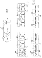
- FIG. 2 there is shown the wiring diagram of a switch K for use in the DC / DC converter, shown in FIG.
- This switch K has a plurality of cells resonant, also called “switching cells”, associated in series with each other.
- the high-voltage switch K comprises n resonance cells, referenced 1a, 1b, ..., 1n.
- Each of these resonance cells comprises two switches K1 and K2, two diodes D1 and D2, an inductor L, a resonance capacitor C and a clipping means M e .
- the diode D1 is connected by its terminal P, by means of interruption K2 (also called switch) and the diode D2 is connected by its terminal N to the switch K1 (also called interruption means).
- An inductor L is connected between the terminal P of the diode D1 and the terminal N of the diode D2. This set D1, D2, K1, K2 and L form what will be called, by the next, "the inductive circuit".
- a resonance capacitor C is connected in parallel on this inductor circuit; a limiter means M e is also connected in parallel to the resonance capacitor.
- This limiter means M e serves to limit the maximum voltage across the capacitor C and to protect voltage switches K1 and K2 and diodes D1 and D2.
- the inductive circuit realized by the diodes D1, D2, the switches K1 and K2 and the inductance L, with, in parallel on this inductor circuit, the resonance capacitor C.
- the clipping means M e n has not been shown because it does not affect the general operation of the resonance cells.
- Closing switches K1 and K2 causes a resonant discharge in the capacitor of resonance C which then yields its energy to the inductor resonance L.
- the main current of the switch K then crosses the switches K1 and K2 and the resonance inductance L of each cell of resonance of the switch K.
- the opening of the switches K1 and K2 of each resonance cell causes the return of the energy of the resonance inductance L towards the resonance capacitor C via the diodes D1 and D2.
- the voltage across the capacitor C has the same polarity as the origin, that is to say, it has the same polarity whatever the state of the switches K1 and K2; the tension at capacitor terminals C does not reverse.
- Figures 4A to 4F show the different phases of circuit operation chopper-depressor, of Figure 3.
- FIG. 4A represents the initial phase of the operation, called the freewheel phase.
- this phase which is the initial phase of operation, the switches K1 and K2 are open, and the diodes D1 and D2 are blocked, while the freewheeling diode D RL is conducting. It's a stable phase. The current across the inductor is zero.
- FIG. 4B shows the second phase of the operation of the chopper-depressor circuit of FIG. 3.
- the switches K1 and K2 are closed.
- the inductance L is then subjected to the voltage E.
- the capacitor C remains charged to E.
- FIG. 4C the third phase of the operation of the circuit of FIG. 3 is shown.
- the freewheeling diode D RL is blocked, the inductance L and the capacitance C come into resonance.
- the current in the inductor increases, while the capacitance is discharged.
- the diodes D1 and D2 go into conduction.
- FIG. 4D the fourth phase of the chopper-step circuit is shown.
- the switches K1 and K2 and the diodes D1 and D2 are conductive.
- the current contained in the inductance L flows freely through K1 / D1 and K2 / D2.
- the current I 0 passes through D1 / K2 and K1 / D2.
- the capacitance C is short-circuited.
- This phase is stable and evolves only at the opening of the switches K1 and K2.
- FIG. 4E shows the fourth phase of circuit operation chopper-down.
- this phase when the switches K1 and K2 are simultaneously opened, a resonance occurs between the inductance L and the capacitance C.
- the capacitor C charges, while the current in inductance L decreases.
- E tension at the terminals of the capacitor C is equal to E, then the freewheeling diode starts.
- FIG. 4F the sixth phase of circuit operation chopper-down.
- capacitor C remains charged to voltage E, while the current in the inductor L decreases linearly.
- the diodes D1 and D2 are blocked and one returns to the initial freewheel phase, represented in Figure 4A.
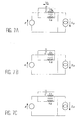
- FIG 5 there is shown another embodiment of the electronic switch high voltage K intended to be used in the DC / DC converter.
- This switch K has, as in the first embodiment, a plurality of resonant cells (or switching cells) connected in series and referenced 2a, 2b, ..., 2n.
- Each of these resonance cells has an inductor circuit consisting of two inductors L1 and L2 connected in series and coupled magnetically.
- the inductive circuit further includes a switch K3 (also called interruption means), connected at the input of the inductor L1, and a diode D3 connected at the output of the inductor L2.
- a resonance capacitor C is connected in parallel on the switch K3 and the inductor L1; it is itself connected in parallel with a clipping means M e .
- FIG. 6 shows the diagram of operation of the cell 2a, in the structure chopper-depressor described above.
- FIG. 6 the following electrical diagram is obtained in FIG. 6, in which the cell 2a receives a voltage E at the input and outputs a current I 0 , represented by the voltage source.
- a freewheeling diode D RL is connected in parallel with the current source.
- FIGS. 7A to 7F there is shown the six different phases of circuit operation of Figure 6.
- the initial phase that is to say the freewheeling phase
- the switch K3 and the diode D3 are blocked, while the freewheeling diode D RL leads. It's a stable phase; K3 and D3 each support a voltage E.
- FIG. 7B schematizes the second operating phase of the step-down chopper circuit of FIG. 6.
- the switch K3 is closed.
- the inductances L1 and L2 are then subjected to the voltage E.
- the resonance capacitance C remains charged to E.
- the secondary of the inductances imposes a voltage - E which keeps the diode D3 blocked.
- This diode D3 then supports a voltage of 2E.
- the current in the freewheeling diode is canceled after a time t, which is equal to L x I 0 / E, which causes, at this instant, the opening of the freewheeling diode D RL .
- FIG. 7C the third phase of operation of the chopper-depressor circuit of FIG. 6 is shown.
- the freewheeling diode is blocked, the inductances L1 and L2 and the capacitance C come into resonance. The current in the inductances increases, while the capacitance C is discharged. When the voltage V C across the capacitance C becomes zero, then the diode D3 comes into conduction.
- FIG. 7D the fourth phase of operation of the chopper-step circuit is shown.
- the switch K3 and the diode D3 are conductive.
- the direct current in the inductances L 1 and L 2 flows freely through the switch K3 and the diode D3.
- the current I 0 passes through this switch and this diode.
- the capacitance C is short-circuited and, consequently, a voltage V C is zero.
- This phase is stable and evolves only when the switches are opened.
- FIG. 7F the sixth phase of circuit operation step-down chopper of Figure 6.
- the capacity C remains loaded at the voltage E, while the current in the inductor decreases linearly; the K3 switch supports a voltage of 2E.
- the diode D3 crashes and we then return to the initial phase of freewheeling.
- the inductance (s) of each of the cells can be coupled with the inductances of other cells, which allows to balance the voltages of the cells.
- FIG. 8 the diagram is represented wiring a switch K intended to be used in the DC / DC converter, shown in FIG.
- This switch K has a plurality of cells resonant, also called “switching cells”, associated in series with each other.
- the high-voltage switch K has n cells resonance, referenced 3a, 3b, ..., 3n.
- Each of these resonance cells has two switches K1 and K2, two diodes D1 and D2, an inductor L, a resonance capacitor C and two clipping means E1 and E2.
- first K1 switch (or means of interruption) is connected at the terminal P of the second diode D2; at the same time, first diode D1 is connected by its terminal N to second switch K2.
- Capacitor C is connected between the P terminal of the D2 diode and the N terminal of the diode D1.
- a first clipping means E1 is connected in parallel on the set consisting of the switch K1 and diode D2 so as to protect this set, in tension.
- Another way to achieve this function is to use an E2 clipper means connected in parallel on the capacitor C so as to limit the maximum voltage at the terminals of the latter.
- An inductor L is connected between the input of the cell and the terminal P of the diode D1, that is to say on the input terminal e of the set consisting of diodes D1, D2, switches K1, K2, clipping means E1, E2 and capacitor C.
- Closing switches K1 and K2 causes a resonant discharge in the capacitor of resonance C which then yields its energy to the inductor resonance L.
- the main current of the switch K then crosses the switches K1 and K2 and the resonance inductance L of each cell of resonance of the high-voltage switch K.
- the opening of the switches K1 and K2 of each resonance cell causes the return of the resonance inductance energy L to the resonance capacitor C via the diodes D1 and D2.
- the voltage across the capacitor C has the same polarity as the origin, that is to say, it has the same polarity whatever the state of the switches K1 and K2; the tension at capacitor terminals C does not reverse.
- Figures 10A to 10F show the different phases of circuit operation step-down chopper, of Figure 9.
- FIG 10A shows the initial phase of operation, called the freewheeling phase.
- the switches K1 and K2 are open and the diodes D1 and D2 are off, while the freewheeling diode Dl1 is conductive. It's a stable phase.
- FIG. 10B the second phase of the operation of the chopper-depressor circuit of FIG. 9 is shown.
- the switches K1 and K2 are closed.
- There is a resonance between the inductance L and the capacitor C in which the current I L flowing in the inductance increases, while the capacitor C discharges.
- FIG. 10C shows the third operating phase of the circuit of FIG. 3.
- the freewheeling diode D rl is blocked, the inductance L is traversed by the current I 0 while the capacitor C is discharged. .
- FIG. 10D the fourth phase of the chopper-step circuit is shown.
- the switches K1 and D2 as well as the diodes D1 and D2 conduct.
- This phase is stable and evolves only when the switches are opened.
- FIG. 10F the sixth phase of operation of the chopper-step circuit is shown.
- the diode D rl free wheel begins, there is a resonance between the inductor L and the capacitor C.
- the voltage V c increases while the current I L in the inductor L decreases.
- this current I L is zero, the diodes D1 and D2 are locked and return to the freewheel phase.
- a high voltage DC / DC converter having a high voltage switch as described previously sees its lifespan increase, by compared to the devices proposed in the prior art.
- the switching cells forming the switch being assembled in series, the switch has the advantage of not being totally inoperative when a component of one of cells is defective.
- the power is processed by a high tension; this makes it possible to manage reduced currents.
- An embodiment on a printed circuit is therefore possible, hence the ease of realization and reduction of costs compared to a very common structure, which requires a mechanical assembly often expensive.
- obtaining frequencies of high division that is to say above 10 kHz, allows to reduce the value of the capacitive filter of output, while maintaining effective filtering.
- parasitic capacitances with environment are included in the capabilities of the different stages of the switch.
- the currents parasites are therefore greatly reduced.
- the energy contained in the parasitic capacitances is recycled in the resonance energy, instead of being totally dissipated in semiconductors, as this is the case in the devices of the prior art.
Landscapes
- Engineering & Computer Science (AREA)
- Power Engineering (AREA)
- Dc-Dc Converters (AREA)
Claims (6)
- Elektronischer Hochspannungsschalter, durchquert von einem Hauptstrom, dadurch gekennzeichnet, dass er wenigstens zwei Schaltzellen (1a, ..., 1n) umfasst, die in Serie geschaltet sind und die Rückführung der Energien der Streukapazitäten sicherstellen, wobei jede dieser Schaltzellen umfasst:wenigstens eine Diode (D1, D2) mit Anschlüssen N und P;wenigstens eine Induktivität (L),wenigstens einen die Streukapazitäten enthaltenden Resonanzkondenstator (C);wenigstens eine Spannungsspitzenwert-Begrenzungseinrichtung (Me); undwenigstens eine Unterbrechungseinrichtung (K1, K2) des Stroms in der Zelle, derartig, dass das Schließen dieser Unterbrechungseinrichtung eine Entladung des Resonanz- und Streukapazitätenkondensators in die Induktivität bewirkt, so dass der Hauptstrom jede Zelle durchquert, und dass das öffnen dieser Unterbrechungseinrichtung das Laden des Resonanz- und Streukapazitätenkondensators aus der Induktivität bewirkt, über die Diode, wobei der genannte Kondensator unabhängig vom jeweiligen Zustand der Unterbrechungseinrichtungen an seinen Anschlüssen eine Spannung derselben Polarität aufweist und die Induktivität unabhängig vom jeweiligen Zustand der Unterbrechungseinrichtungen von einem Strom derselben Richtung durchquert wird.
- Schalter nach Anspruch 1, dadurch gekennzeichnet, dass jede Zelle (1., ..., 1n) eine erste und eine zweite Unterbrechungseinrichtung (K1, K2) und eine erste und eine zweite Diode (D1, D2) umfasst, wobei die erste Unterbrechungseinrichtung (K2) mit dem Anschluss P der ersten Diode (D1) verbunden ist, die zweite Unterbrechungseinrichtung (K1) mit dem Anschluss N der zweiten Diode (D2) verbunden ist, und die Induktivität (L) der Zelle zwischen dem Anschluss P der ersten Diode und dem Anschluss N der zweiten Diode angeschlossen ist, wobei dieses Unterbrechung-Dioden-Induktivitäts-System einen zu dem Resonanzkondensator (C) parallelgeschalteten Induktionskreis bildet, der seinerseits zu der Spitzenwertbegrenzungseinrichtung (Me) parallelgeschaltet ist.
- Schalter nach Anspruch 1, dadurch gekennzeichnet, das jede Zelle (2a, ..., 2n) eine erste und eine zweite Induktivität (L1, L2) umfasst, in Serie geschaltet und magnetisch gekoppelt, wobei die erste Induktivität (L1 ) außerdem mit der Unterbrechungseinrichtung (K3) und die zweite Induktivität (L2) mit der Diode (D3) verbunden ist, und dieses einen Induktionskreis bildende Unterbrechung-Diode-Induktivitäten-System einerseits durch einen Anschluss zwischen den beiden Induktivitäten und andererseits durch die Unterbrechungseinrichtung mit dem Resonanzkondensator verbunden ist, der seinerseits zu der Spitzenwertbegrenzungseinrichtung parallelgeschaltet ist.
- Schalter nach Anspruch 1, dadurch gekennzeichnet, dass jede Zelle umfasst:wobei der Resonanzkondensator (C) zwischen dem Anschluss P der zweiten Diode und dem Anschluss N der ersten Diode angeschlossen ist, und die Induktivität (L) zwischen dem Eingang der Zelle und dem Anschluss P der ersten Diode angeschlossen ist.eine erste und eine zweite Unterbrechungseinrichtung (K1, K2);eine erste und eine zweite Diode (D1, D2), wobei die erste Unterbrechungseinrichtung (K1)mit dem Anschluss der zweiten Diode (D2) verbunden ist, und die zweite Unterbrechungseinrichtung (K2) mit dem Anschluss N der ersten Diode (D1) verbunden ist;eine erste oder eine zweite Spannungsspitzenwert-Begrenzungseinrichtung (E1, E2), jeweils parallelgeschaltet zwischen dem Eingang der ersten Unterbrechungseinrichtung und dem Anschluss N der zweiten Diode oder parallelgeschaltet zum Kondensator;
- Schalter nach einem der Ansprüche 1 bis 4, dadurch gekennzeichnet, dass die Induktivität(en) jeder Zelle magnetisch mit den Induktivitäten der anderen Zellen gekoppelt ist (sind).
- Gleichstrom/Hochspannungsgleichstrom-Umspanner, eine Freilaufdiode (DRL), eine Induktivität (B) und eine Kapazität (A) umfassend, dadurch gekennzeichnet, dass er einen elektronischen Hochspannungsschalter nach einem der Ansprüche 1 bis 5 umfasst.
Applications Claiming Priority (2)
| Application Number | Priority Date | Filing Date | Title |
|---|---|---|---|
| FR9716070 | 1997-12-18 | ||
| FR9716070A FR2773010B1 (fr) | 1997-12-18 | 1997-12-18 | Interrupteur haute tension realise a partir de cellules resonantes connectees en serie |
Publications (2)
| Publication Number | Publication Date |
|---|---|
| EP0928057A1 EP0928057A1 (de) | 1999-07-07 |
| EP0928057B1 true EP0928057B1 (de) | 2003-09-24 |
Family
ID=9514777
Family Applications (1)
| Application Number | Title | Priority Date | Filing Date |
|---|---|---|---|
| EP98403161A Expired - Lifetime EP0928057B1 (de) | 1997-12-18 | 1998-12-15 | Hochspannungsschalter aus reihengeschalteten resonanten Zellen |
Country Status (3)
| Country | Link |
|---|---|
| EP (1) | EP0928057B1 (de) |
| DE (1) | DE69818415T2 (de) |
| FR (1) | FR2773010B1 (de) |
Cited By (1)
| Publication number | Priority date | Publication date | Assignee | Title |
|---|---|---|---|---|
| US11251716B2 (en) * | 2019-11-21 | 2022-02-15 | Turbo Power Systems Ltd. | Electricity distribution networks |
Families Citing this family (1)
| Publication number | Priority date | Publication date | Assignee | Title |
|---|---|---|---|---|
| US10651838B2 (en) | 2017-01-13 | 2020-05-12 | Siemens Aktiengesellschaft | DC power switching assembly and method |
Family Cites Families (2)
| Publication number | Priority date | Publication date | Assignee | Title |
|---|---|---|---|---|
| FR2279250A1 (fr) * | 1974-07-16 | 1976-02-13 | Inst Im Gm Krzhizhanovsko | Dispositif de protection contre des surtensions des thyristors d'un convertisseur a haute tension commande |
| DE3822991A1 (de) * | 1988-07-07 | 1990-01-11 | Olympia Aeg | Hochspannungsschalter |
-
1997
- 1997-12-18 FR FR9716070A patent/FR2773010B1/fr not_active Expired - Fee Related
-
1998
- 1998-12-15 EP EP98403161A patent/EP0928057B1/de not_active Expired - Lifetime
- 1998-12-15 DE DE69818415T patent/DE69818415T2/de not_active Expired - Lifetime
Cited By (1)
| Publication number | Priority date | Publication date | Assignee | Title |
|---|---|---|---|---|
| US11251716B2 (en) * | 2019-11-21 | 2022-02-15 | Turbo Power Systems Ltd. | Electricity distribution networks |
Also Published As
| Publication number | Publication date |
|---|---|
| FR2773010A1 (fr) | 1999-06-25 |
| DE69818415D1 (de) | 2003-10-30 |
| EP0928057A1 (de) | 1999-07-07 |
| FR2773010B1 (fr) | 2000-01-14 |
| DE69818415T2 (de) | 2004-06-24 |
Similar Documents
| Publication | Publication Date | Title |
|---|---|---|
| EP0898357B1 (de) | Gleichstromwandlervorrichtung | |
| EP2258037B1 (de) | Stromversorgung mit nichtisolierter dc-dc-teilung | |
| EP0082071B1 (de) | Einrichtung für die Umschaltung einer mit mindestens einem gesteuerten Schalter versehenen Gleichspannungsquelle und Kommutierungshilfsschaltung für eine solche Einrichtung | |
| EP2011220A2 (de) | Verbesserte isolierleistungstransfereinrichtung | |
| EP0680245A2 (de) | Statischer Wandler mit gesteuertem Schalter und Steuerungsschaltung | |
| EP2355331A1 (de) | Wandlervorrichtung und mit einer solchen Vorrichtung ausgerüstete unterbrechungslose Versorgung | |
| FR2845211A1 (fr) | Systeme et procede de conversion vers un facteur de puissance eleve | |
| EP2645569B1 (de) | Steuervorrichtung, die in einem Stromzuführungssystem mit Partitionierung verwendet wird | |
| FR2738417A1 (fr) | Convertisseur de tension continue a commutation douce | |
| FR2627644A1 (fr) | Convertisseur continu-continu, sans pertes de commutation, notamment pour alimentation continue haute frequence ou pour amplificateur a tube a ondes progressives | |
| EP2320553A2 (de) | Stromumwandlungsvorrichtung und unterbrechungsfreie Stromversorgung, die eine solche Vorrichtung umfasst | |
| EP0928057B1 (de) | Hochspannungsschalter aus reihengeschalteten resonanten Zellen | |
| EP0788219B1 (de) | Steuervorrichtung für eine ZVS-Schaltung | |
| WO2008099087A2 (fr) | Generateur et procede de generation de haute tension continue, depoussiereur utilisant ce generateur | |
| EP0670624B1 (de) | Angepasstes Schaltnetzteil um Kommutierungen bei niedriger Spannung auszuführen | |
| EP0924844B1 (de) | Aus einer Reihenschaltung von quasiresonanten Zellen aufgebauter Hochspannungsschalter | |
| EP0101629B1 (de) | Statische elektrische Energieumwandlungseinheit mit Halbleitern | |
| FR2773011A1 (fr) | Interrupteur haute tension realise a partir de cellules a deux interrupteurs aides a la fermeture et a l'ouverture, connectees en serie | |
| EP0184493B1 (de) | Gleichstromregler mit Taktschalter und Transformator | |
| FR2632134A1 (fr) | Procede de linearisation pour convertisseur continu-continu et dispositifs mettant en oeuvre ce procede | |
| EP1444768B1 (de) | Verfahren und einrichtung zur transformation einer gleichspannung und verwendung der einrichtung | |
| FR2860660A1 (fr) | Convertisseur elevateur de tension | |
| EP0405653B1 (de) | Elektrische Energie-Leistungskonverter, deren Kommutierung durch eine aktive Steuerung der Versorgungsspannung der Spannungsumpolschaltung unterstützt wird | |
| EP3276812B1 (de) | Isolierter dc-dc-wandler und elektrische batterie, die einen solchen isolierten dc-dc-wandler umfasst | |
| EP0392420B1 (de) | Gleichstromschaltwandler |
Legal Events
| Date | Code | Title | Description |
|---|---|---|---|
| PUAI | Public reference made under article 153(3) epc to a published international application that has entered the european phase |
Free format text: ORIGINAL CODE: 0009012 |
|
| AK | Designated contracting states |
Kind code of ref document: A1 Designated state(s): CH DE GB IT LI |
|
| AX | Request for extension of the european patent |
Free format text: AL;LT;LV;MK;RO;SI |
|
| 17P | Request for examination filed |
Effective date: 19991122 |
|
| AKX | Designation fees paid |
Free format text: CH DE GB IT LI |
|
| 17Q | First examination report despatched |
Effective date: 20010828 |
|
| GRAH | Despatch of communication of intention to grant a patent |
Free format text: ORIGINAL CODE: EPIDOS IGRA |
|
| RAP1 | Party data changed (applicant data changed or rights of an application transferred) |
Owner name: COMMISSARIAT A L'ENERGIE ATOMIQUE |
|
| GRAS | Grant fee paid |
Free format text: ORIGINAL CODE: EPIDOSNIGR3 |
|
| GRAA | (expected) grant |
Free format text: ORIGINAL CODE: 0009210 |
|
| AK | Designated contracting states |
Kind code of ref document: B1 Designated state(s): CH DE GB IT LI |
|
| REG | Reference to a national code |
Ref country code: GB Ref legal event code: FG4D Free format text: NOT ENGLISH |
|
| REG | Reference to a national code |
Ref country code: CH Ref legal event code: EP |
|
| REF | Corresponds to: |
Ref document number: 69818415 Country of ref document: DE Date of ref document: 20031030 Kind code of ref document: P |
|
| GBT | Gb: translation of ep patent filed (gb section 77(6)(a)/1977) |
Effective date: 20040115 |
|
| PLBE | No opposition filed within time limit |
Free format text: ORIGINAL CODE: 0009261 |
|
| STAA | Information on the status of an ep patent application or granted ep patent |
Free format text: STATUS: NO OPPOSITION FILED WITHIN TIME LIMIT |
|
| 26N | No opposition filed |
Effective date: 20040625 |
|
| PGFP | Annual fee paid to national office [announced via postgrant information from national office to epo] |
Ref country code: GB Payment date: 20141218 Year of fee payment: 17 Ref country code: CH Payment date: 20141215 Year of fee payment: 17 |
|
| PGFP | Annual fee paid to national office [announced via postgrant information from national office to epo] |
Ref country code: DE Payment date: 20141211 Year of fee payment: 17 Ref country code: IT Payment date: 20141223 Year of fee payment: 17 |
|
| REG | Reference to a national code |
Ref country code: DE Ref legal event code: R119 Ref document number: 69818415 Country of ref document: DE |
|
| REG | Reference to a national code |
Ref country code: CH Ref legal event code: PL |
|
| GBPC | Gb: european patent ceased through non-payment of renewal fee |
Effective date: 20151215 |
|
| PG25 | Lapsed in a contracting state [announced via postgrant information from national office to epo] |
Ref country code: LI Free format text: LAPSE BECAUSE OF NON-PAYMENT OF DUE FEES Effective date: 20151231 Ref country code: GB Free format text: LAPSE BECAUSE OF NON-PAYMENT OF DUE FEES Effective date: 20151215 Ref country code: DE Free format text: LAPSE BECAUSE OF NON-PAYMENT OF DUE FEES Effective date: 20160701 Ref country code: CH Free format text: LAPSE BECAUSE OF NON-PAYMENT OF DUE FEES Effective date: 20151231 |
|
| PG25 | Lapsed in a contracting state [announced via postgrant information from national office to epo] |
Ref country code: IT Free format text: LAPSE BECAUSE OF NON-PAYMENT OF DUE FEES Effective date: 20151215 |