EP0788219B1 - Steuervorrichtung für eine ZVS-Schaltung - Google Patents
Steuervorrichtung für eine ZVS-Schaltung Download PDFInfo
- Publication number
- EP0788219B1 EP0788219B1 EP97400199A EP97400199A EP0788219B1 EP 0788219 B1 EP0788219 B1 EP 0788219B1 EP 97400199 A EP97400199 A EP 97400199A EP 97400199 A EP97400199 A EP 97400199A EP 0788219 B1 EP0788219 B1 EP 0788219B1
- Authority
- EP
- European Patent Office
- Prior art keywords
- switch
- switching
- current
- load
- decision
- Prior art date
- Legal status (The legal status is an assumption and is not a legal conclusion. Google has not performed a legal analysis and makes no representation as to the accuracy of the status listed.)
- Expired - Lifetime
Links
Images


Classifications
-
- H—ELECTRICITY
- H02—GENERATION; CONVERSION OR DISTRIBUTION OF ELECTRIC POWER
- H02M—APPARATUS FOR CONVERSION BETWEEN AC AND AC, BETWEEN AC AND DC, OR BETWEEN DC AND DC, AND FOR USE WITH MAINS OR SIMILAR POWER SUPPLY SYSTEMS; CONVERSION OF DC OR AC INPUT POWER INTO SURGE OUTPUT POWER; CONTROL OR REGULATION THEREOF
- H02M7/00—Conversion of ac power input into dc power output; Conversion of dc power input into ac power output
- H02M7/42—Conversion of dc power input into ac power output without possibility of reversal
- H02M7/44—Conversion of dc power input into ac power output without possibility of reversal by static converters
- H02M7/48—Conversion of dc power input into ac power output without possibility of reversal by static converters using discharge tubes with control electrode or semiconductor devices with control electrode
- H02M7/53—Conversion of dc power input into ac power output without possibility of reversal by static converters using discharge tubes with control electrode or semiconductor devices with control electrode using devices of a triode or transistor type requiring continuous application of a control signal
- H02M7/537—Conversion of dc power input into ac power output without possibility of reversal by static converters using discharge tubes with control electrode or semiconductor devices with control electrode using devices of a triode or transistor type requiring continuous application of a control signal using semiconductor devices only, e.g. single switched pulse inverters
- H02M7/538—Conversion of dc power input into ac power output without possibility of reversal by static converters using discharge tubes with control electrode or semiconductor devices with control electrode using devices of a triode or transistor type requiring continuous application of a control signal using semiconductor devices only, e.g. single switched pulse inverters in a push-pull configuration
- H02M7/53803—Conversion of dc power input into ac power output without possibility of reversal by static converters using discharge tubes with control electrode or semiconductor devices with control electrode using devices of a triode or transistor type requiring continuous application of a control signal using semiconductor devices only, e.g. single switched pulse inverters in a push-pull configuration with automatic control of output voltage or current
-
- Y—GENERAL TAGGING OF NEW TECHNOLOGICAL DEVELOPMENTS; GENERAL TAGGING OF CROSS-SECTIONAL TECHNOLOGIES SPANNING OVER SEVERAL SECTIONS OF THE IPC; TECHNICAL SUBJECTS COVERED BY FORMER USPC CROSS-REFERENCE ART COLLECTIONS [XRACs] AND DIGESTS
- Y02—TECHNOLOGIES OR APPLICATIONS FOR MITIGATION OR ADAPTATION AGAINST CLIMATE CHANGE
- Y02B—CLIMATE CHANGE MITIGATION TECHNOLOGIES RELATED TO BUILDINGS, e.g. HOUSING, HOUSE APPLIANCES OR RELATED END-USER APPLICATIONS
- Y02B70/00—Technologies for an efficient end-user side electric power management and consumption
- Y02B70/10—Technologies improving the efficiency by using switched-mode power supplies [SMPS], i.e. efficient power electronics conversion e.g. power factor correction or reduction of losses in power supplies or efficient standby modes
Definitions
- the present invention relates to a control device a circuit comprising a resonance inverter intended to supply the minus a load with an inductive component.
- Such circuits are also known as structures ZVS (ZVS being the English initials set for "Zero Voltage Switch ").
- the circuit which interests us in the context of the present invention is an inverter of the type comprising at least two switches Q 1 , Q 2 of the transistor type (bipolar, Mosfet or IGBT) connected in series across a power supply. DC voltage -E, + E.
- the switching transistors Q 1 and Q 2 are controlled at a predetermined frequency so as to be alternately conductive. They transmit the energy from the supply voltage to a load Z via a resonance inductor L and a resonance capacitor C connected in series at the junction point J of the two switches.
- two freewheeling diodes D 1 and D 2 each mounted in parallel on one of the two transistors are necessary.
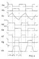
- FIG. 2 illustrates a chronogram of operation of the ZVS half-bridge structure in Figure 1:
- a first control strategy consists in allowing the switch to be closed only when the voltage across its terminals vanishes.
- Such a strategy is for example described in the document FR 2,499,789.
- the major drawback of this type of strategy is that, if for reasons of load variations or input voltage or starting problems, the current I L in the load is not sufficient to charge or to discharge the capacitors C 1 and C 2 , then the voltage across the terminals of the switches does not cancel and the switches do not close.
- the current is not sufficient to drive the freewheeling diode and the other switch, the voltage of which is not s never cancels, cannot be closed.
- a second control strategy consists in allowing the closing of a switch only for a fixed and predetermined duration T M after having opened the other switch. If, for reasons identical to those mentioned above, the current IL is not sufficient for the charges or discharges of the switching aid capacitors, the switches will be closed with a residual voltage across the terminals of the capacitors. It follows an overcurrent in the switches, detrimental to their operation, and can even go as far as their destruction.
- a control strategy is ill-suited to the use of bipolar transistors as switches. Indeed, the bipolar transistors have a certain response time, called storage time, which is difficult to control and which can be of the order of twice the duration T M. We can certainly remedy this by imposing that the instant from which the duration T M runs is no longer the instant of opening of a transistor, but the instant when the current in the transistor is canceled, but it is then necessary to provide special circuits.
- the document EP -A- 0 320 410 describes a control device a resonance inverter in which the closing of the switches is controlled by the zero current crossing in the load.
- the object of the present invention is to propose a device using a new ordering strategy that does not show the aforementioned drawbacks.
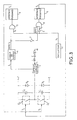
- FIG. 3 represents a possible embodiment of a control device for the implementation of the control strategy used by the invention.
- FIG. 3 shows the ZVS half-bridge structure of FIG. 1, all the other elements of the figure being specific to the control device for this structure.
- FIG. 4 represents the different curves in FIG. 4, representing the shape of the signals over time at different points of the control device and of the ZVS structure.
- Two switching decision signals S 1 and S 2 are created for the opening and closing of each of the switches Q 1 , Q 2 .
- the curves 4a and 4b in FIG. 4 illustrate the shape of these two decision signals over time.
- Each signal S 1 or S 2 has two states 1 or 0 representative of a decision to open or close the associated switch.
- the signal S 1 goes from state 1 to state 0 when one decides to open the switch Q 1 , and goes from state 0 to state 1 when one decides to close it.
- One of the two decision signals, for example S 1 can be obtained from an oscillator 1 (FIG. 3) generating a rectangular signal, and the signal S 2 can be obtained by means of an inverter 2 receiving on its input the signal S 1 .
- curve 4c in FIG. 4 illustrates the shape of the current I L in the load.
- a current sensor 3 in series with the load makes it possible to take this current I L.
- a logic signal SENS_I L with two states is created, representative of the direction of the current I L in the load.
- the curve 4d in FIG. 4 represents the signal SENS_I L obtained when the current I L is compared with the zero reference.
- the current I L can be delivered to the input of a Schmidt trigger 4 which has an internal reference slightly greater than zero so as to obtain a signal L SENS_I slight phase advance with respect to the current I L.
- the particular combination of this signal SENS_I L with the switching decision signals S 1 and S 2 will make it possible to generate two control signals T 1 and T 2 of the switches Q 1 and Q 2 .
- a first control signal T 1 is generated by performing the logical AND function of the decision signal S 1 and of the signal SENS_I L.
- a first AND gate 5 with two inputs and an output connected to a power interface 6 allow the generation of such a control signal T 1 .
- a second control signal T 2 is generated by performing the logical AND function of the decision signal S 2 and of a signal SENS_I L complementary to SENS_I L , obtained using an inverter 7 and the shape of which is shown on the curve 4e of FIG. 4.
- a second AND gate 8 followed by a power interface 9 allow the generation of the signal T 2 .
- the curves 4f and 4g respectively represent the control signals T 1 and T 2 obtained.
- the opening command (change from 1 to 0) of the switch Q 1 takes place as soon as that the opening decision is made.
- the decision is made to close the switch Q 1 (passage from 0 to 1 of the signal T 1 )
- the closing command T 1 does not operate effectively until the current I L has changed direction .
- a similar reasoning can be carried out on the switch Q 2 .
- the previous assembly has the advantage of never stopping, even in the event of a wrong order. Indeed, suppose for example that the current I L is too weak. The switches will still be closed as soon as a change of direction in the current is detected.
- Such an arrangement also makes it possible to return more quickly to a state stable when mounting is subject to external disturbance.
- the charging or discharging times of the switching aid capacitors C 1 and C 2 can be much more variable here than in the case of a dead time command.
- the control device has a current transformer TR used for the production of the control currents of the base of the transistors Q 1 and Q 2 . More specifically, a primary winding TR P of the transformer TR is connected in series between the load and the common junction point between the transistors Q 1 , Q 2 , the freewheeling diodes D 1 , D 2 and the capacitors for assisting switching C 1 , C 2 .
- a first secondary winding TR S1 of the transformer TR is connected between the emitter of the transistor Q 1 and to the positive terminal of a first DC voltage supply E 1 , the negative terminal of which is connected to the base of the transistor Q 1 .
- a second secondary winding TR S2 of the transformer TR is connected between the emitter of the transistor Q 2 and a second DC voltage supply E 2 , the second terminal of which is connected to the base of the transistor Q 2 .
- a third secondary winding TR S3 is connected between the ground of the circuit and the anode of a diode D S3 .
- the cathode of the diode is connected to the source of an FET 2 field effect transistor which serves as an electronic switch.
- a fourth secondary winding TR S4 of the transformer TR is connected to the source of a field effect transistor FET 1 via a diode D S4 .
- the windings TR S3 and TR S4 are coupled respectively to the windings TR S2 and TR S1 .
- the polarizations of the different windings are indicated by the points placed on the sides of the windings.
- This signal B is delivered on the one hand on the gate of the transistor FET 2 , and on the other hand, after inversion by an inverter 11, on the gate of the FET transistor 1 .
- phase 4 ⁇ After phase 4 ⁇ , cycle 1 ⁇ to 4 ⁇ is repeated.
- the transformer described above, makes it possible to obtain galvanic isolation between on the one hand, the controlled part comprising the load Z and the elements in series with it, the transistors Q 1 , Q 2 , the diodes D 1 , D 2 , and the capacitors C 1 , C 2 , and on the other hand the control part comprising the oscillator 10, the switches FET 1 , FET 2 and the diodes D S3 , D S4 .
- the transformer described above, also allows self-supply of the base of the transistors Q 1 , Q 2 , without supply of energy by an external supply.
- control process as just described is good understood applicable to any ZVS structure derived from the half-bridge structure shown in Figure 1.
- the ordering process can also be generalized to a ZVS full bridge structure, comprising two pairs of transistors, or a ZVS structure comprising any number of pairs of transistors.
- Figure 7 illustrates the electrical diagram of a ZVS structure in full bridge:
Claims (4)
- Vorrichtung zum Steuern einer Schaltung, die einen Resonanz-Wechselrichter enthält, der wenigstens eine Last versorgen soll, die eine induktive Komponente (L) enthält, wobei der Wechselrichter von dem Typ ist, der wenigstens umfaßt:wobei der gemeinsame Verbindungspunkt zwischen den beiden Schalttransistoren, die Freilaufdioden und die Kondensatoren mit einem Anschluß der Last in Serie geschaltet sind; wobei die Vorrichtung umfaßt:ein Paar Schalttransistoren (Q1, Q2), die zwischen die Anschlüsse einer Gleichspannungsversorgung (-E, +E; O, E) in der Weise in Serie geschaltet sind, daß zwei Ein/Aus-Schalter gebildet werden, die unter der Wirkung der Steuervorrichtung abwechselnd leiten;zwei Freilaufdioden (D1, D2), die jeweils zu einem der zwei Transistoren parallelgeschaltet sind;zwei Schalthilfskondensatoren (C1, C2), die jeweils zu einem der zwei Transistoren parallelgeschaltet sind;wobei die Vorrichtung dadurch gekennzeichnet ist, daß sie einen Stromtransformator (TR) aufweist, der umfaßt:erste Mittel, die für jeden Ein/Aus-Schalter (Q1, Q2) ein Schalt-Entscheidungssignal (B,
B ) mit zwei Zuständen, die eine Entscheidung zum Öffnen oder zum Schließen des Ein/Aus-Schalters repräsentieren, liefern, wobei die beiden Schalt-Entscheidungssignale jeweils über eine Leistungsschnittstelle den beiden Ein/Aus-Schaltern zugeordnet sind, wobei die beiden Schalt-Entscheidungssignale entgegengesetzte Phase besitzen, so daß abwechselnd das periodische Öffnen und Schließen jedes Ein/Aus-Schalters bestimmt wird;zweite Mittel, die ermöglichen, Änderungen der Stromrichtung (IL) in der Last zu erfassen;wobei die Vorspannungen der verschiedenen Wicklungen in der Weise gewählt sind, daß das Öffnen eines Ein/Aus-Schalters erfolgt, sobald das zugeordnete Schalt-Entscheidungssignal in einem Zustand ist, der die Entscheidung zum Öffnen repräsentiert, und in der Weise, daß das Schließen eines Ein/Aus-Schalters erfolgt, wenn das zugeordnete Schalt-Entscheidungssignal in einem Zustand ist, der die Entscheidung zum Schließen repräsentiert, und im wesentlichen dann, wenn der Strom in der Last seine Richtung geändert hat.eine Primärwicklung (TRP), die zwischen die Last und den gemeinsamen Verbindungspunkt zwischen den Ein/Aus-Schaltern (Q1, Q2), die Freilaufdioden (D1, D2) und die SchaltHilfskondensatoren (C1, C2) in Serie geschaltet ist;eine erste Sekundärwicklung (TRS1), die zwischen den Emitter eines (Q1) der zwei Ein/Aus-Schalter und den ersten Anschluß einer ersten Gleichspannungsversorgung (E1) geschaltet ist, wobei der zweite Versorgungsanschluß mit der Basis des Ein/Aus-Schalters (Q1) verbunden ist;eine zweite Sekundärwicklung (TRS2), die zwischen den Emitter des anderen (Q2) Ein/Aus-Schalters und den ersten Anschluß einer zweiten Gleichspannungsversorgung (E2) geschaltet ist, wobei der zweite Versorgungsanschluß mit der Basis dieses anderen Ein/Aus-Schalters (Q2) verbunden ist;eine dritte (TRS3) und eine vierte (TRS4) Sekundärwicklung, die mit der zweiten bzw. der ersten Sekundärwicklung verbunden sind, wobei die dritten und vierten Sekundärwicklungen (TRS3, TRS4) zwischen Masse und eine der Leistungsschnittstellen geschaltet sind; - Vorrichtung nach Anspruch 1, dadurch gekennzeichnet, daß das Schließen eines Ein/Aus-Schalters dann, wenn das zugeordnete Schalt-Entscheidungssignal in einem Zustand ist, der die Entscheidung zum Schließen repräsentiert, mit einer geringen Phasenvoreilung in bezug auf den Zeitpunkt erfolgt, zu dem der Strom in der Last seine Richtung ändert.
- Vorrichtung nach einem der vorhergehenden Ansprüche, dadurch gekennzeichnet, daß die Leistungsschnittstelle einen elektronischen Schalter (FET2, FET1) sowie eine Diode (DS3, DS4) enthält, wobei jeder elektronische Schalter durch eines der beiden Schalt-Entscheidungssignale (B,
B ) gesteuert wird. - Vorrichtung nach einem der vorhergehenden Ansprüche, dadurch gekennzeichnet, daß die ersten Mittel einen Oszillator enthalten.
Applications Claiming Priority (2)
| Application Number | Priority Date | Filing Date | Title |
|---|---|---|---|
| FR9601059 | 1996-01-30 | ||
| FR9601059A FR2744300B1 (fr) | 1996-01-30 | 1996-01-30 | Procede et dispositif de commande d'un circuit zvs |
Publications (2)
| Publication Number | Publication Date |
|---|---|
| EP0788219A1 EP0788219A1 (de) | 1997-08-06 |
| EP0788219B1 true EP0788219B1 (de) | 2001-06-06 |
Family
ID=9488608
Family Applications (1)
| Application Number | Title | Priority Date | Filing Date |
|---|---|---|---|
| EP97400199A Expired - Lifetime EP0788219B1 (de) | 1996-01-30 | 1997-01-28 | Steuervorrichtung für eine ZVS-Schaltung |
Country Status (5)
| Country | Link |
|---|---|
| US (1) | US5841646A (de) |
| EP (1) | EP0788219B1 (de) |
| DE (1) | DE69705078T2 (de) |
| ES (1) | ES2160898T3 (de) |
| FR (1) | FR2744300B1 (de) |
Families Citing this family (10)
| Publication number | Priority date | Publication date | Assignee | Title |
|---|---|---|---|---|
| US6246598B1 (en) * | 2000-08-02 | 2001-06-12 | Polarity, Inc. | High-voltage modulator system |
| AR030511A1 (es) * | 2000-12-22 | 2003-08-20 | Patricio Lagos Lehuede | Un inversor o convertidor por inyeccion de corriente provisto de un circuito cuya frecuencia de generacion de la tension alterna esta ajustada por la frecuencia de resonancia de la carga, ciclo a ciclo, sin retardos |
| US6696675B2 (en) * | 2001-08-10 | 2004-02-24 | Tocco, Inc. | Induction heating system for internal combustion engine |
| FR2850216B1 (fr) * | 2003-01-21 | 2005-04-08 | Brandt Ind | Generateur d'alimentation d'un circuit oscillant, notamment pour table de cuisson par induction. |
| DE10303779A1 (de) * | 2003-01-31 | 2004-07-22 | Daimlerchrysler Ag | Vorrichtung zum Laden und Entladen piezoelektrischer Elemente |
| TWI325737B (en) * | 2006-12-01 | 2010-06-01 | Full bridge driver | |
| US7504905B1 (en) * | 2008-01-30 | 2009-03-17 | The United States Of America As Represented By The Secretary Of The Navy | Method for coupling a direct current power source across a dielectric membrane or other non-conducting membrane |
| RU2448406C1 (ru) * | 2010-10-12 | 2012-04-20 | Государственное образовательное учреждение высшего профессионального образования "Уфимский государственный авиационный технический университет" | Способ управления резонансным инвертором со встречно-параллельными диодами |
| DE102014226716A1 (de) * | 2014-12-19 | 2016-06-23 | Dialog Semiconductor (Uk) Limited | Spannungsverdoppler und Spannungsverdopplungsverfahren zur Verwendung im PMW-Modus |
| US10993292B2 (en) * | 2017-10-23 | 2021-04-27 | Whirlpool Corporation | System and method for tuning an induction circuit |
Family Cites Families (6)
| Publication number | Priority date | Publication date | Assignee | Title |
|---|---|---|---|---|
| US4342076A (en) * | 1981-02-12 | 1982-07-27 | Westinghouse Electric Corp. | Transistor turn off current sensing circuit |
| JP2585511B2 (ja) * | 1985-07-16 | 1997-02-26 | 株式会社豊田中央研究所 | インバ−タ駆動装置 |
| FR2624671B1 (fr) * | 1987-12-09 | 1990-12-14 | Merlin Gerin | Dispositif de commande d'un interrupteur statique |
| US5027263A (en) * | 1988-09-16 | 1991-06-25 | Kyushu University | Switching power source means |
| DE3901034C1 (en) * | 1989-01-14 | 1990-07-19 | Danfoss A/S, Nordborg, Dk | Inverter |
| FR2644948B1 (fr) * | 1989-03-23 | 1993-11-05 | Electricite De France | Circuit electrique de conversion d'energie |
-
1996
- 1996-01-30 FR FR9601059A patent/FR2744300B1/fr not_active Expired - Fee Related
-
1997
- 1997-01-28 DE DE69705078T patent/DE69705078T2/de not_active Expired - Lifetime
- 1997-01-28 ES ES97400199T patent/ES2160898T3/es not_active Expired - Lifetime
- 1997-01-28 EP EP97400199A patent/EP0788219B1/de not_active Expired - Lifetime
- 1997-01-30 US US08/790,996 patent/US5841646A/en not_active Expired - Lifetime
Also Published As
| Publication number | Publication date |
|---|---|
| FR2744300A1 (fr) | 1997-08-01 |
| DE69705078D1 (de) | 2001-07-12 |
| EP0788219A1 (de) | 1997-08-06 |
| FR2744300B1 (fr) | 1998-03-06 |
| ES2160898T3 (es) | 2001-11-16 |
| US5841646A (en) | 1998-11-24 |
| DE69705078T2 (de) | 2002-03-14 |
Similar Documents
| Publication | Publication Date | Title |
|---|---|---|
| EP0082071B1 (de) | Einrichtung für die Umschaltung einer mit mindestens einem gesteuerten Schalter versehenen Gleichspannungsquelle und Kommutierungshilfsschaltung für eine solche Einrichtung | |
| EP0788219B1 (de) | Steuervorrichtung für eine ZVS-Schaltung | |
| EP0680245A2 (de) | Statischer Wandler mit gesteuertem Schalter und Steuerungsschaltung | |
| EP1564876B1 (de) | Schweisseinrichtung mit sanfschaltendem Quasi-resonanzwechselrichter | |
| EP2320553B1 (de) | Stromumwandlungsvorrichtung und unterbrechungsfreie Stromversorgung, die eine solche Vorrichtung umfasst | |
| FR2627644A1 (fr) | Convertisseur continu-continu, sans pertes de commutation, notamment pour alimentation continue haute frequence ou pour amplificateur a tube a ondes progressives | |
| EP3346597A1 (de) | Wechselstrom-gleichstrom-wandler | |
| EP0329571B1 (de) | Schaltungsanordnung zur Überwachung der Entmagnetisierung für einen Sperrwandler mit primärseitiger und secundärseitiger Regelung | |
| EP0977346A1 (de) | Gleichstrom-Gleichstromwandler | |
| FR2658674A1 (fr) | Convertisseur continu-continu a commutation a tension nulle. | |
| CA2042485A1 (fr) | Procede de limitation d'une surcharge base sur la technique de controle pwm (ou lc3) et dispositif electronique de mise en oeuvre de ce procede | |
| EP0743742B1 (de) | Leistungsfaktorverbesserung für eine gleichgerichtete Leistungsversorgung | |
| FR3106457A1 (fr) | Procédé et dispositif de conversion d’une tension avec commutation douce des interrupteurs. | |
| EP0261018B1 (de) | Spannungsfrequenzselbstgeführter Konverter | |
| EP0320410A1 (de) | Anordnung zum Steuern eines statischen Schalters | |
| EP2940849A2 (de) | Elektrische stromversorgung und steuerverfahren einer solchen elektrischen stromversorgung | |
| EP0928057B1 (de) | Hochspannungsschalter aus reihengeschalteten resonanten Zellen | |
| FR2809234A1 (fr) | Thyristor dual, thyristor diode dual, thysistor, thysistor diode, convertisseur et interrupteur | |
| FR2674723A1 (fr) | Circuit d'alimentation pour une charge electrique comme une lampe a decharge, notamment pour projecteur de vehicule et projecteur de vehicule utilisant un tel circuit. | |
| EP1324478A2 (de) | Hochspannungswandler mit schneller Antwortzeit | |
| EP3829063A1 (de) | Bidirektionale schaltersteuerung | |
| EP0014108A1 (de) | Zeilenablenkschaltung für Fernsehempfänger | |
| FR2969862A1 (fr) | Systeme de conversion d'energie a decoupage, formant un bras de hacheur de tension. | |
| FR2744857A1 (fr) | Convertisseur d'energie electrique a inverseurs resonants "demi-periode" | |
| FR2668020A1 (fr) | Circuit d'alimentation pour une charge electrique comme une lampe a decharge, notamment pour projecteur de vehicule et projecteur de vehicule utilisant un tel circuit. |
Legal Events
| Date | Code | Title | Description |
|---|---|---|---|
| PUAI | Public reference made under article 153(3) epc to a published international application that has entered the european phase |
Free format text: ORIGINAL CODE: 0009012 |
|
| AK | Designated contracting states |
Kind code of ref document: A1 Designated state(s): BE DE ES FR GB IT NL |
|
| 17P | Request for examination filed |
Effective date: 19971121 |
|
| 17Q | First examination report despatched |
Effective date: 19990331 |
|
| GRAG | Despatch of communication of intention to grant |
Free format text: ORIGINAL CODE: EPIDOS AGRA |
|
| GRAG | Despatch of communication of intention to grant |
Free format text: ORIGINAL CODE: EPIDOS AGRA |
|
| GRAH | Despatch of communication of intention to grant a patent |
Free format text: ORIGINAL CODE: EPIDOS IGRA |
|
| RAP1 | Party data changed (applicant data changed or rights of an application transferred) |
Owner name: BRANDT COOKING |
|
| GRAH | Despatch of communication of intention to grant a patent |
Free format text: ORIGINAL CODE: EPIDOS IGRA |
|
| GRAA | (expected) grant |
Free format text: ORIGINAL CODE: 0009210 |
|
| AK | Designated contracting states |
Kind code of ref document: B1 Designated state(s): BE DE ES FR GB IT NL |
|
| REF | Corresponds to: |
Ref document number: 69705078 Country of ref document: DE Date of ref document: 20010712 |
|
| ITF | It: translation for a ep patent filed |
Owner name: JACOBACCI & PERANI S.P.A. |
|
| GBT | Gb: translation of ep patent filed (gb section 77(6)(a)/1977) |
Effective date: 20010907 |
|
| REG | Reference to a national code |
Ref country code: ES Ref legal event code: FG2A Ref document number: 2160898 Country of ref document: ES Kind code of ref document: T3 |
|
| REG | Reference to a national code |
Ref country code: GB Ref legal event code: IF02 |
|
| PLBE | No opposition filed within time limit |
Free format text: ORIGINAL CODE: 0009261 |
|
| STAA | Information on the status of an ep patent application or granted ep patent |
Free format text: STATUS: NO OPPOSITION FILED WITHIN TIME LIMIT |
|
| 26N | No opposition filed | ||
| REG | Reference to a national code |
Ref country code: FR Ref legal event code: TP |
|
| NLS | Nl: assignments of ep-patents |
Owner name: BRANDT INDUSTRIES Effective date: 20071018 |
|
| REG | Reference to a national code |
Ref country code: GB Ref legal event code: 732E |
|
| PGFP | Annual fee paid to national office [announced via postgrant information from national office to epo] |
Ref country code: NL Payment date: 20110128 Year of fee payment: 15 |
|
| PGFP | Annual fee paid to national office [announced via postgrant information from national office to epo] |
Ref country code: GB Payment date: 20110222 Year of fee payment: 15 Ref country code: BE Payment date: 20110218 Year of fee payment: 15 |
|
| REG | Reference to a national code |
Ref country code: FR Ref legal event code: CD Owner name: FAGORBRANDT SAS, FR Effective date: 20110826 |
|
| REG | Reference to a national code |
Ref country code: ES Ref legal event code: PC2A Owner name: FAGORBRANDT SAS Effective date: 20111021 |
|
| REG | Reference to a national code |
Ref country code: NL Ref legal event code: TD Effective date: 20111221 |
|
| REG | Reference to a national code |
Ref country code: DE Ref legal event code: R082 Ref document number: 69705078 Country of ref document: DE Representative=s name: PRINZ & PARTNER MBB PATENTANWAELTE RECHTSANWAE, DE Effective date: 20120322 Ref country code: DE Ref legal event code: R082 Ref document number: 69705078 Country of ref document: DE Representative=s name: PRINZ & PARTNER PATENTANWAELTE RECHTSANWAELTE, DE Effective date: 20120322 Ref country code: DE Ref legal event code: R081 Ref document number: 69705078 Country of ref document: DE Owner name: FAGORBRANDT SAS, FR Free format text: FORMER OWNER: BRANDT INDUSTRIES, RUEIL MALMAISON, FR Effective date: 20120322 |
|
| PGFP | Annual fee paid to national office [announced via postgrant information from national office to epo] |
Ref country code: IT Payment date: 20120130 Year of fee payment: 16 |
|
| BERE | Be: lapsed |
Owner name: FAGORBRANDT SAS Effective date: 20120131 |
|
| REG | Reference to a national code |
Ref country code: NL Ref legal event code: V1 Effective date: 20120801 |
|
| GBPC | Gb: european patent ceased through non-payment of renewal fee |
Effective date: 20120128 |
|
| PG25 | Lapsed in a contracting state [announced via postgrant information from national office to epo] |
Ref country code: GB Free format text: LAPSE BECAUSE OF NON-PAYMENT OF DUE FEES Effective date: 20120128 |
|
| PG25 | Lapsed in a contracting state [announced via postgrant information from national office to epo] |
Ref country code: BE Free format text: LAPSE BECAUSE OF NON-PAYMENT OF DUE FEES Effective date: 20120131 |
|
| PG25 | Lapsed in a contracting state [announced via postgrant information from national office to epo] |
Ref country code: NL Free format text: LAPSE BECAUSE OF NON-PAYMENT OF DUE FEES Effective date: 20120801 |
|
| PGFP | Annual fee paid to national office [announced via postgrant information from national office to epo] |
Ref country code: DE Payment date: 20130211 Year of fee payment: 17 |
|
| PGFP | Annual fee paid to national office [announced via postgrant information from national office to epo] |
Ref country code: FR Payment date: 20131231 Year of fee payment: 18 Ref country code: ES Payment date: 20140224 Year of fee payment: 18 |
|
| REG | Reference to a national code |
Ref country code: DE Ref legal event code: R119 Ref document number: 69705078 Country of ref document: DE |
|
| REG | Reference to a national code |
Ref country code: DE Ref legal event code: R119 Ref document number: 69705078 Country of ref document: DE Effective date: 20140801 |
|
| PG25 | Lapsed in a contracting state [announced via postgrant information from national office to epo] |
Ref country code: DE Free format text: LAPSE BECAUSE OF NON-PAYMENT OF DUE FEES Effective date: 20140801 |
|
| REG | Reference to a national code |
Ref country code: FR Ref legal event code: ST Effective date: 20150930 |
|
| PG25 | Lapsed in a contracting state [announced via postgrant information from national office to epo] |
Ref country code: FR Free format text: LAPSE BECAUSE OF NON-PAYMENT OF DUE FEES Effective date: 20150202 |
|
| REG | Reference to a national code |
Ref country code: ES Ref legal event code: FD2A Effective date: 20160226 |
|
| PG25 | Lapsed in a contracting state [announced via postgrant information from national office to epo] |
Ref country code: ES Free format text: LAPSE BECAUSE OF NON-PAYMENT OF DUE FEES Effective date: 20150129 |
|
| REG | Reference to a national code |
Ref country code: FR Ref legal event code: TP Owner name: GROUPE BRANDT, FR Effective date: 20160420 |
|
| REG | Reference to a national code |
Ref country code: FR Ref legal event code: GC Effective date: 20160426 |
|
| PG25 | Lapsed in a contracting state [announced via postgrant information from national office to epo] |
Ref country code: IT Free format text: LAPSE BECAUSE OF NON-PAYMENT OF DUE FEES Effective date: 20140128 |