EP1324478A2 - Hochspannungswandler mit schneller Antwortzeit - Google Patents
Hochspannungswandler mit schneller Antwortzeit Download PDFInfo
- Publication number
- EP1324478A2 EP1324478A2 EP02354199A EP02354199A EP1324478A2 EP 1324478 A2 EP1324478 A2 EP 1324478A2 EP 02354199 A EP02354199 A EP 02354199A EP 02354199 A EP02354199 A EP 02354199A EP 1324478 A2 EP1324478 A2 EP 1324478A2
- Authority
- EP
- European Patent Office
- Prior art keywords
- switch
- circuit
- oscillator
- voltage
- capacitor
- Prior art date
- Legal status (The legal status is an assumption and is not a legal conclusion. Google has not performed a legal analysis and makes no representation as to the accuracy of the status listed.)
- Withdrawn
Links
Images


Classifications
-
- H—ELECTRICITY
- H02—GENERATION; CONVERSION OR DISTRIBUTION OF ELECTRIC POWER
- H02M—APPARATUS FOR CONVERSION BETWEEN AC AND AC, BETWEEN AC AND DC, OR BETWEEN DC AND DC, AND FOR USE WITH MAINS OR SIMILAR POWER SUPPLY SYSTEMS; CONVERSION OF DC OR AC INPUT POWER INTO SURGE OUTPUT POWER; CONTROL OR REGULATION THEREOF
- H02M3/00—Conversion of dc power input into dc power output
- H02M3/02—Conversion of dc power input into dc power output without intermediate conversion into ac
- H02M3/04—Conversion of dc power input into dc power output without intermediate conversion into ac by static converters
- H02M3/10—Conversion of dc power input into dc power output without intermediate conversion into ac by static converters using discharge tubes with control electrode or semiconductor devices with control electrode
- H02M3/145—Conversion of dc power input into dc power output without intermediate conversion into ac by static converters using discharge tubes with control electrode or semiconductor devices with control electrode using devices of a triode or transistor type requiring continuous application of a control signal
- H02M3/155—Conversion of dc power input into dc power output without intermediate conversion into ac by static converters using discharge tubes with control electrode or semiconductor devices with control electrode using devices of a triode or transistor type requiring continuous application of a control signal using semiconductor devices only
Definitions
- the present invention relates to the production of a high voltage oscillator circuit, i.e. capable of operating with supply voltages up to several hundred volts.
- An example of application of the present invention relates to supply systems intended to provide regulated DC voltage.
- the systems to transformer which have the disadvantage of being heavy, bulky and expensive, and converter type systems with cutting.
- Switching power supplies have drawbacks noticeable dissipation caused by the fact that the switch switching is often hard switching (transistor MOS or IGBT), and the absence of voltage supplied from the start or circuit connection. It is indeed generally necessary that an auxiliary power supply of a control circuit provide sufficient energy to operate the switch switching the supply voltage.
- An example of feeding where we use a high voltage oscillator concerns the field of fluorescent lamps compact (CFL).
- the fluorescent tube supply is generally obtained by means of a controlled H-shaped half-bridge, either by means of a transformer or by means of a integrated circuit oscillator. In the latter case, we then have a voltage reference problem for the transistor control of the upper branch of the bridge, which imposes the use of a level shifter.
- the invention will be described below more particularly in connection with an application to a circuit Power. Note, however, that this applies more generally in all areas where a high oscillator voltage may be required. For example, it could be applications with induction energy transfer, such as wireless battery chargers or hot plates by induction.
- the invention aims to propose a high oscillator voltage capable of starting as soon as power is applied, i.e. as soon as it receives a supply voltage.
- the invention also aims to facilitate filtering possible circuit entry to reduce disturbance electromagnetic.
- the invention also aims to propose an oscillator with low dissipation compared to known switching systems in power supplies.
- the invention further aims to minimize the bulk of the oscillator.
- the invention further aims to solve the reference problems voltage for controlling the switching components.
- the oscillator has a single resonant circuit.
- control circuit has no supply circuit auxiliary.
- said first switch is closed for periods of charging of a capacitor of the series resonant circuit, and is open during a resonance phase.
- the first switch is controlled by comparing the voltage across the resonant circuit with respect to a threshold predetermined.
- control of the second switch is carried out by delaying the instant of closure of this switch relative to the end of conduction of the first switch.
- said switches are bidirectional in current and in voltage.
- said switches are unidirectional.
- the oscillator has a polarized freewheeling diode of reverse to the second switch.
- the resonance phase includes a first discharge cycle of said capacitor through the second switch and a second cycle of discharging said capacitor through said freewheeling diode.
- the second switch consists of a thyristor whose the anode is connected on the first switch side.
- the first switch consists of a bipolar transistor NPN type normally closed by connecting its base and its collector by means of a resistor, the emitter of the bipolar transistor being connected to the resonant circuit.
- the invention also provides a supply circuit continuous with a high voltage oscillator.
- an output capacitor is connected, in parallel with two rectifier diodes in series at the second switch.
- a first rectifying diode connects one end of the circuit resonating to an electrode of the second switch and to an electrode positive of the output capacitor, the anode of the first rectifier diode being connected to the resonant circuit and to the cathode of a second rectifier diode connected to the diode freewheel.
- the polarity of the output voltage is chosen according to the electrode of the output capacitor to which is connected the reference of the supply voltage.
- the supply circuit includes a control circuit having role of delaying the boot time of the second switch depending on the output voltage.
- FIG. 1 very schematically represents a embodiment of an oscillator according to the present invention.
- a first switch K1 is in series with a capacitor C and an inductance L between two terminals 1 and 2 application of a supply or input voltage Ve.
- a diode D is connected in parallel with the resonant circuit CL.
- a second switch K2 is also in parallel on the resonant circuit C-L, therefore in parallel with diode D, the anode of diode D being connected to terminal 2.
- a feature of the invention is to use switches K1 and K2 of the normally closed type. Another characteristic of the invention is to share the same circuit resonant series (inductance L and capacitor C) for all circuit operating phases.
- the switches K1 and K2 are controlled by a circuit 3 providing two separate HS and LS signals for respective switches K1 and K2.
- the switches K1 and K2 are bidirectional in voltage and in current, that is to say capable of holding a high voltage in the state open whatever its polarity and drive in both sense in the closed state.
- the diode D is omitted. If the input voltage is alternating, the circuit then works during all the alternations.
- the switches K1 and K2 are one-way switches, (at less functionally by means of the control circuit 3).
- the input voltage Ve is a voltage alternative (for example, the mains voltage electric) the oscillator only works during half-waves positive (or negative) of alternative food.
- switch K2 could be bidirectional in current and unidirectional in voltage (case of a MOS transistor). In this case, the diode D is short-circuited by the closing of switch K2.
- the circuit 3 is shaped so to prevent, as soon as the oscillator is powered up, a simultaneous conduction of switches K1 and K2 which would have result of shorting the power supply.
- the switch K1 essentially used to charge the capacitor C of the resonant circuit from the voltage Ve while switch K2 allows the resonant circuit to be used for discharge capacitor C, using the freewheeling diode D if switch K2 is unidirectional.
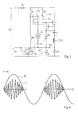
- FIGS. 2A to 2D illustrate, by chronograms, the operation of a high voltage oscillator according to the invention.
- FIG. 2A represents an example of the shape of the current I in the resonant circuit.
- Figure 2B illustrates the appearance of the voltage V across the capacitor C.
- FIG. 2C illustrates the closing periods of switch K1.
- Figure 2D illustrates periods of closure of switch K2.
- diode D could be made up of another switch synchronized, to be combined with switch K2 (stray diode) if the latter is fast enough, or be replaced by the conduction of switch K2 if the latter is bidirectional while running.
- control circuit 3 must force opening of switch K2, switch K1 remaining open for the whole resonance phase.
- a second phase of operation of the oscillator of the invention consists of recharging the capacitor C from the supply voltage Ve. Indeed, part of the energy initially stored in capacitor C has been dissipated during the previous resonance phase or consumed by the load (not shown). The voltage level V is therefore, at time t4, lower than the level of time t0.
- the purpose of the second phase of operation is to recharge the capacitor C at its initial level.
- the switch K1 being a switch normally closed, it naturally becomes conductive as soon as its opening is no longer forced by the control circuit (instant t5).
- the capacitor C is therefore recharged through inductance L in series.
- the current drawn from the source of supply voltage here corresponds to half-wave sinusoidal (instant t5 to t6).
- the switch K1 is chosen so that its opening occurs naturally when the current flowing through it is canceled to avoid overvoltages linked to this opening.
- the command of the switch K1 is particularly simplified as well that filtering against electromagnetic interference generated by the cutting of the current drawn from food.
- control circuit 3 forces the opening of switch K2 so to prevent the two switches K1 and K2 from conducting simultaneously.
- intervals between instants t6 and t0 and t4 and t5 can be deleted if necessary. It depends no only control circuit but also energy consumed by the powered circuit.
- a first advantage is that opening the switch K2 takes place while no current flows through it (instant t2). It is therefore a switching to zero current, which leads to easier filtering if necessary.
- oscillator can operate as well as with alternating input voltage than with a continuous input voltage.
- Another advantage is that a single resonant circuit (therefore, a single inductive element) suffices for the two phases of resonance linked to the recharging of the oscillating circuit.
- An advantage of using switches normally closed is that it reduces the losses of switching. Another advantage is that it also reduces control currents required, and does not require auxiliary power supply to start the circuit.
- FIG. 3 represents an oscillator according to the invention where the control circuit has been functionally illustrated. Note that this can nevertheless correspond to a practical realization, even if it does not constitute a mode of preferred implementation due to local power requirements logic gates and amplifiers used.
- switches K1 and K2 unidirectional. This unidirectional character was symbolized by diodes D1 and D2 respectively in series with each of these switches, the respective anodes of diodes D1 and D2 being directed to terminal 1 for applying the voltage Ve assumed to be the positive terminal.
- a comparator 10 receiving, on its inverting input (-), the voltage across the resonant circuit and, on its non-inverting input (+), a fixed threshold voltage, for example, by a resistive divider bridge R1-R2 connected between terminals 1 and 2, the midpoint of the series association of the resistors R1-R2 being connected to the non-inverting input of the comparator 10.
- the output of the comparator 10 is combined by an OR type door 11 with the result of current detection.
- the exit from gate 11 prevents the conduction of switch K1.
- a delay element can be provided 13 shifting the activation of switch K2 by relative to the instant of closing of the switch K1.
- the delay ⁇ of circuit 13 is chosen to wait for the end of conduction of switch K1 before authorizing the closing of the switch K2.
- Figure 4 shows the electrical diagram of another embodiment of a high voltage oscillator.
- the switch K1 of normally closed type consists of a bipolar transistor T1 type NPN whose base and collector are connected by a ignition resistance R3.
- the emitter of transistor T1 is connected at node 4 and the collector of transistor T1 is connected to the terminal 1.
- the switch K2 here consists of a thyristor Th whose anode is connected to node 4 and whose cathode is connected at terminal 2.
- Comparator 10 consists of a transistor bipolar T2 of type NPN whose base is connected to the midpoint series association of resistors R1 and R2, including collector is connected to the base of transistor T1, and whose the transmitter is connected to node 4.
- the current detector 12 (which detects the current here in diode D and not in the entire oscillating circuit as in Figure 3) consists of a bipolar transistor T3 of NPN type whose collector is connected to the base of transistor T1 and whose transmitter is connected to node 4, the base of the transistor T3 being connected to the cathode of diode D which is not no longer directly connected to node 4.
- Transistor T3 works in switching (blocked-saturated) and can therefore be considered, when driving, as a diode (base-emitter junction) in series with diode D between terminals 2 and 4 for the freewheeling function. In addition, while driving, he blocks transistor T1 by diverting its base current.
- the OR function (11, Figure 3) is performed by direct interconnection of the collectors of the T2 transistors and T3 at the base of transistor T1.
- the retarding element preventing the conduction of the thyristor Th when transistor T1 is on is here consisting of a current source 15 in series with a Cr capacitor connected between terminals 4 and 2.
- the point middle of this serial association is connected to the trigger of the thyristor Th.
- the capacitor Cr At the end of the resonance of the lower stage, that is to say as soon as the transistor T1 is made conductive (instant t5), the capacitor Cr is charged at constant current by source 15. This generates the desired delay for priming thyristor Th.
- the capacitor Cr prevents ignition untimely thyristor under the effect of the voltage rise at the end of the resonance. Indeed, when a current flows in diode D (between times t2 and t3, figure 2), the Cr capacitor is negatively charged. So when the voltage reappears across the thyristor Th, its trigger is negatively polarized, which prevents its initiation.
- FIG. 5 represents an embodiment of a supply circuit based on a high voltage oscillator such as previously described. It is a diet providing a continuous output voltage Vs from a voltage alternative or continuous input Fri. A Dr diode monoalternation rectification is provided at the input of the circuit. The voltage Vs is taken from terminals 20, 21 of a capacitor low filtering voltage Cf whose positive electrode is connected to the cathode of the triac Th of the oscillator of the invention. In the application to a supply circuit, the load of the oscillator, i.e. the capacitor Cf is interposed, associated with two diodes D3 and D4.
- Diode D3 connects the cathode of thyristor Th at the inductance electrode L opposite to capacitor C, the anode of diode D3 being connected to inductance L.
- Diode D4 connects the anode of diode D3 (therefore inductance L) at the anode of diode D, the anode of diode D4 and the anode of diode D being connected together to ground 21.
- the capacitor Cf is charged during all the half-waves of the resonance, i.e. during periods when the thyristor Th leads, during the periods when the diode leads, as well as during the conduction periods of transistor T1.
- the charging circuit of the capacitor Cf includes diode D4, inductance L, capacitor C and thyristor Th.
- the charging circuit of the capacitor Cf comprises the diode D, transistor T3, capacitor C, inductance L and diode D3.
- a control circuit 25 (driver) is provided to delay each oscillator period as a function of the output voltage.
- the role of the control circuit 25 is to add an additional delay between times t6 and t0 depending of a measurement of the output voltage Vs, in order to control this voltage on a predetermined setpoint. Without control circuit, the voltage Vs would increase uncontrollably if the energy was not consumed by a load connected to the terminals of the capacitor Cf.
- the control circuit 25 can be produced from of conventional components, for example by means of amplifiers operational. Its realization is within the reach of the man of the profession based on the functional indications given above.
- the output terminal OUT of circuit 25 is connected to the Th thyristor trigger to control the delay of sound boot.
- Circuit 25 has its supply terminals (VCC and GND) connected to terminals 20 and 21 of capacitor Cf.
- a optional current amplifier 30 has been illustrated in series with resistance R3.
- This current amplifier (buffer) is functionally constituted by a switch 31 connected between resistance R3 and the base of transistor T1.
- Switch 31 is controlled by a comparator 32 whose non-inverting input (+) is connected to the midpoint between resistors R1 and R2 and whose inverting input (-) is connected to the emitter of the transistor T3.
- Comparator 32 is supplied between resistance R3 and the emitter of transistor T3.
- the current amplifier 30 illustrated by figure 5 replaces the transistor T2 of the figure 4. In practice, it may be a Darlington montage produced from bipolar transistors.
- the power circuit of Figure 5 can provide a positive or negative output voltage Vs. It depends only from the terminal used between terminals 20 and 21 for connect the reference of the supply voltage Ve. In taking for example an alternating voltage Ve and a connection from the mains phase to terminal 1, the neutral of the power supply alternative can be connected to terminal 20 or terminal 21 according to the desired sign for the voltage Vs. If the neutral is connected to terminal 20, the negative electrode 21 of the capacitor Cf will present a more negative potential, the voltage Vs will be thus negative. If the neutral of the AC supply is connected to terminal 21 as shown in Figure 5, the Vs voltage will be positive.
- FIG. 5 has been described in relation with a voltage charge of the capacitor Cf. We will note however, this supply circuit also applies to a current load (for example, to form a circuit of an induction hob). This result is permitted as long as the charging current is sinusoidal.
- the control circuit 25 then controls the number of excitation current pulses from the inductive plate.
- a power supply circuit using an oscillator high voltage according to the invention has many benefits.
- a first advantage is the possibility of operating from an alternative or continuous diet without cause modification of the structure of the supply circuit.
- Another advantage is to allow feeding positive or negative without modifying the circuit structure power supply, but simply by changing the terminal connection of the reference potential of the input voltage. This advantage is particularly noticeable, for example, when one wishes to order triacs by negative currents.
- Another advantage of the supply circuit the invention is that it provides continuous power not isolated, which makes it possible to order triacs in particular.
- Another advantage of the present invention is that the power circuit starts as soon as it is energized.
- the oscillator of the invention does not need of a particular command to start operating. This is related to the fact that the switches used are switches normally closed, which is a characteristic essential of the invention. Although circuit 25 is not supplied when the supply circuit is switched on, this does not prevent the high voltage oscillator from starting to function.
- Another advantage is that the circuit allows, when they are necessary, the use of size sector filters lower, thanks to current resonance.
- the frequency of the high voltage oscillator of the invention is significantly higher than the frequency of alternative food.
- the oscillator of the invention chops or cuts the current in relation to the power supply alternative.
- the resonant frequency of the circuit is fixed by the respective dimensions of capacitor C and inductance L, as well as the delays expected for priming of thyristor Th (instant t6 to t0 of FIG. 2).
- the switch is not expected to be delayed K1, that is to say between the instants t4 and t5 of FIGS. 2.
- FIG. 6 illustrates the operation of the circuit of FIG. 5 under an input voltage Ve alternative.
- FIG. 6 represents the shape of the current I in the inductance L and the shape of the alternating voltage Ve.
- the oscillator of the invention does not only works during positive half-waves Ve, i.e. it causes the capacitor Cf to charge that during these positive alternations. Inside these, we can consider that the oscillator of the invention performs a switching the AC supply voltage to charge the capacitor Cf.
- FIG. 6 has been drawn without respect for scale, particularly with regard to the frequency of the oscillations of the current I which is in practice significantly higher than the frequency of the voltage Ve.
- Each current oscillation period I corresponds to the period (t6-t5) illustrated in Figure 2.
- a resonance frequency of several tens of kilo-hertz for example, 80 kHz leading to a frequency of splitting on the order of 35 to 40 kHz.
- normally closed switches can be used at the instead of transistor T1 and thyristor Th.
- a trigger-open thyristor (GTO) and normally closed is a preferred embodiment for its low cost compared to a high voltage MOS transistor or a IGBT type transistor.
- GTO thyristor normally closed is described in US Patent 6,323,718 (B3706).
Landscapes
- Engineering & Computer Science (AREA)
- Power Engineering (AREA)
- Inductance-Capacitance Distribution Constants And Capacitance-Resistance Oscillators (AREA)
- Electronic Switches (AREA)
Applications Claiming Priority (2)
| Application Number | Priority Date | Filing Date | Title |
|---|---|---|---|
| FR0117037 | 2001-12-28 | ||
| FR0117037A FR2834392A1 (fr) | 2001-12-28 | 2001-12-28 | Oscillateur haute tension ayant un temps de reaction rapide |
Publications (2)
| Publication Number | Publication Date |
|---|---|
| EP1324478A2 true EP1324478A2 (de) | 2003-07-02 |
| EP1324478A3 EP1324478A3 (de) | 2003-08-13 |
Family
ID=8871078
Family Applications (1)
| Application Number | Title | Priority Date | Filing Date |
|---|---|---|---|
| EP02354199A Withdrawn EP1324478A3 (de) | 2001-12-28 | 2002-12-30 | Hochspannungswandler mit schneller Antwortzeit |
Country Status (3)
| Country | Link |
|---|---|
| US (1) | US6894575B2 (de) |
| EP (1) | EP1324478A3 (de) |
| FR (1) | FR2834392A1 (de) |
Cited By (1)
| Publication number | Priority date | Publication date | Assignee | Title |
|---|---|---|---|---|
| CN103812338A (zh) * | 2012-11-14 | 2014-05-21 | 罗伯特·博世有限公司 | 用于调节直流电压变换器的测量电路 |
Families Citing this family (2)
| Publication number | Priority date | Publication date | Assignee | Title |
|---|---|---|---|---|
| EP2523336B1 (de) | 2005-08-16 | 2020-10-07 | MKS Instruments, Inc. | Ladungsresonantes Netzteil für einen Ozonisator |
| DE102013021305B3 (de) * | 2013-12-19 | 2014-10-30 | Krohne Messtechnik Gmbh | Schaltungsanordnung zur Temperaturüberwachung und kalorimetrisches Massedurchflussmessgerät |
Citations (5)
| Publication number | Priority date | Publication date | Assignee | Title |
|---|---|---|---|---|
| GB1160803A (en) * | 1966-03-23 | 1969-08-06 | Landis & Gyr Ag | Controlled Rectifier Inverter Circuits |
| US4488214A (en) * | 1982-11-15 | 1984-12-11 | Spellman High Voltage Electronics Corp. | High-power, high-frequency inverter system with combined digital and analog control |
| US4967332A (en) * | 1990-02-26 | 1990-10-30 | General Electric Company | HVIC primary side power supply controller including full-bridge/half-bridge driver |
| EP0758160A1 (de) * | 1995-08-09 | 1997-02-12 | Sony Corporation | Treiberimpuls beschränkter Schaltkreis |
| US6002213A (en) * | 1995-10-05 | 1999-12-14 | International Rectifier Corporation | MOS gate driver circuit with analog input and variable dead time band |
Family Cites Families (3)
| Publication number | Priority date | Publication date | Assignee | Title |
|---|---|---|---|---|
| US4677347A (en) * | 1984-10-26 | 1987-06-30 | Olympus Optical, Co., Ltd. | Electronic flash |
| US5099202A (en) | 1990-02-26 | 1992-03-24 | General Electric Company | Phase shift generator |
| US5227961A (en) | 1990-02-26 | 1993-07-13 | General Electric Company | Symmetrical delay circuit |
-
2001
- 2001-12-28 FR FR0117037A patent/FR2834392A1/fr not_active Withdrawn
-
2002
- 2002-12-19 US US10/325,432 patent/US6894575B2/en not_active Expired - Lifetime
- 2002-12-30 EP EP02354199A patent/EP1324478A3/de not_active Withdrawn
Patent Citations (5)
| Publication number | Priority date | Publication date | Assignee | Title |
|---|---|---|---|---|
| GB1160803A (en) * | 1966-03-23 | 1969-08-06 | Landis & Gyr Ag | Controlled Rectifier Inverter Circuits |
| US4488214A (en) * | 1982-11-15 | 1984-12-11 | Spellman High Voltage Electronics Corp. | High-power, high-frequency inverter system with combined digital and analog control |
| US4967332A (en) * | 1990-02-26 | 1990-10-30 | General Electric Company | HVIC primary side power supply controller including full-bridge/half-bridge driver |
| EP0758160A1 (de) * | 1995-08-09 | 1997-02-12 | Sony Corporation | Treiberimpuls beschränkter Schaltkreis |
| US6002213A (en) * | 1995-10-05 | 1999-12-14 | International Rectifier Corporation | MOS gate driver circuit with analog input and variable dead time band |
Cited By (2)
| Publication number | Priority date | Publication date | Assignee | Title |
|---|---|---|---|---|
| CN103812338A (zh) * | 2012-11-14 | 2014-05-21 | 罗伯特·博世有限公司 | 用于调节直流电压变换器的测量电路 |
| CN103812338B (zh) * | 2012-11-14 | 2018-11-02 | 罗伯特·博世有限公司 | 用于调节直流电压变换器的测量电路 |
Also Published As
| Publication number | Publication date |
|---|---|
| FR2834392A1 (fr) | 2003-07-04 |
| EP1324478A3 (de) | 2003-08-13 |
| US20030132810A1 (en) | 2003-07-17 |
| US6894575B2 (en) | 2005-05-17 |
Similar Documents
| Publication | Publication Date | Title |
|---|---|---|
| EP0496654B1 (de) | Dimmer mit minimalen Filterungsverlusten für eine Leistungslast | |
| EP0680245A2 (de) | Statischer Wandler mit gesteuertem Schalter und Steuerungsschaltung | |
| FR2587156A1 (fr) | Circuit de pompe de charge pour commander des transistors mos a canal n | |
| FR2511830A1 (fr) | Generateur pour la mise et le maintien en fonction d'une charge, et procede d'allumage d'une lampe a conduction ionique | |
| FR3034924A1 (fr) | Convertisseur alternatif-continu a limitation du courant d'appel | |
| FR2627644A1 (fr) | Convertisseur continu-continu, sans pertes de commutation, notamment pour alimentation continue haute frequence ou pour amplificateur a tube a ondes progressives | |
| FR2587155A1 (fr) | Circuit de commande pour des transistors mos de puissance a canal n montes dans des etages push-pull | |
| FR2734429A1 (fr) | Module interrupteur et d'alimentation-application au demarrage d'un tube fluorescent | |
| EP0390699A1 (de) | Versorgungsschaltung einer Bogenlampe, insbesondere eines Automobilscheinwerfers | |
| EP0820141A2 (de) | Nullspannungsansteuerung einer hybriden Brückenschaltung | |
| EP3345456B1 (de) | Elektronischer wandler und beleuchtungssystem mit solch einem wandler | |
| FR2621751A1 (fr) | Procede de production d'une basse tension continue stabilisee | |
| EP1324478A2 (de) | Hochspannungswandler mit schneller Antwortzeit | |
| EP0798838A1 (de) | Schaltung zur Verbesserung des Leistungsfaktors mit doppelter Entladung | |
| FR3068546A1 (fr) | Convertisseur ac/dc reversible a triacs | |
| EP0413806A1 (de) | Anlauf- und versorgungsschaltung für leuchtstofflampen mit vorheizbaren elektroden | |
| EP1061650A1 (de) | Bistabiler Zweirichtungs-Hochspannungsschalter | |
| EP2781023B1 (de) | Leistungsvariator | |
| FR2557399A1 (fr) | Amplificateur de puissance lineaire | |
| EP1473818A1 (de) | Treiber eines Triacs | |
| EP1435691B1 (de) | Schaltungsanordnung zur Steuerung eines Triacs ohne galvanische Trennung | |
| EP1434340B1 (de) | Isolierte Niederspannungsversorgung | |
| CA2033030C (fr) | Circuit d'alimentation electrique d'une charge unidirectionnelle telle qu'un magnetron | |
| EP2268107A1 (de) | Schaltung zur Steuerung einer Beleuchtungsvorrichtung für Leuchtdioden | |
| FR3122793A1 (fr) | Circuit électronique avec thyristor |
Legal Events
| Date | Code | Title | Description |
|---|---|---|---|
| PUAI | Public reference made under article 153(3) epc to a published international application that has entered the european phase |
Free format text: ORIGINAL CODE: 0009012 |
|
| PUAL | Search report despatched |
Free format text: ORIGINAL CODE: 0009013 |
|
| AK | Designated contracting states |
Designated state(s): AT BE BG CH CY CZ DE DK EE ES FI FR GB GR IE IT LI LU MC NL PT SE SI SK TR |
|
| AX | Request for extension of the european patent |
Extension state: AL LT LV MK RO |
|
| AK | Designated contracting states |
Designated state(s): AT BE BG CH CY CZ DE DK EE ES FI FR GB GR IE IT LI LU MC NL PT SE SI SK TR |
|
| AX | Request for extension of the european patent |
Extension state: AL LT LV MK RO |
|
| 17P | Request for examination filed |
Effective date: 20040203 |
|
| AKX | Designation fees paid |
Designated state(s): DE FR GB IT |
|
| STAA | Information on the status of an ep patent application or granted ep patent |
Free format text: STATUS: THE APPLICATION IS DEEMED TO BE WITHDRAWN |
|
| 18D | Application deemed to be withdrawn |
Effective date: 20070703 |