EP0014108A1 - Zeilenablenkschaltung für Fernsehempfänger - Google Patents
Zeilenablenkschaltung für Fernsehempfänger Download PDFInfo
- Publication number
- EP0014108A1 EP0014108A1 EP80400012A EP80400012A EP0014108A1 EP 0014108 A1 EP0014108 A1 EP 0014108A1 EP 80400012 A EP80400012 A EP 80400012A EP 80400012 A EP80400012 A EP 80400012A EP 0014108 A1 EP0014108 A1 EP 0014108A1
- Authority
- EP
- European Patent Office
- Prior art keywords
- capacitor
- switch
- circuit
- thyristor
- series
- Prior art date
- Legal status (The legal status is an assumption and is not a legal conclusion. Google has not performed a legal analysis and makes no representation as to the accuracy of the status listed.)
- Withdrawn
Links
Images
Classifications
-
- H—ELECTRICITY
- H03—ELECTRONIC CIRCUITRY
- H03K—PULSE TECHNIQUE
- H03K4/00—Generating pulses having essentially a finite slope or stepped portions
- H03K4/06—Generating pulses having essentially a finite slope or stepped portions having triangular shape
- H03K4/08—Generating pulses having essentially a finite slope or stepped portions having triangular shape having sawtooth shape
- H03K4/83—Generating pulses having essentially a finite slope or stepped portions having triangular shape having sawtooth shape using as active elements semiconductor devices with more than two PN junctions or with more than three electrodes or more than one electrode connected to the same conductivity region
Definitions
- the invention relates to a line-scanning circuit of a television receiver, comprising thyristors.
- the fundamental horizontal scanning circuit essentially comprises: a source, a first switching device composed of the inductance constituted by the deflection coil connected in series with a high capacity capacitor, and a first thyristor-diode couple operating as a scanning switch , and a second switching device composed of a reactive circuit consisting of an inductance and a capacitive network, and of a second thyristor-diode couple passing an oscillating current through the scanning switch, so as to allow the cancellation of the current in the first thyristor while at the same time ensuring the transfer of energy from the source to the scanning coil associated with its capacitor.
- the trigger of the second thyristor is coupled to the receiver's line oscillator.
- the invention relates to how to generate the trigger signal of the first thyristor operating as a scanning switch.
- the trigger is directly attacked by an active circuit, such as the line oscillator (horizontal).
- an active circuit such as the line oscillator (horizontal).
- a capacitive coupling it is necessary to have a continuous supply voltage of high value (25 volts).
- a strongly negative DC supply voltage (- 25 volts) becomes necessary. At start-up it is difficult to quickly obtain these voltages.
- Another solution consists in using the signal formed on the inductor joining the second switching device to the DC supply voltage source.
- This signal which is positive prior to the conduction of the first thyristor, becomes negative during the recovery time of the latter and the line feed.
- the sampling of this signal requires an auxiliary winding coupled to this inductor joining the scanning circuit to the power source.
- active regulation is used in series with said inductance. But in this case, the voltage available for triggering the trigger drops to zero during the opening period of the active regulating element, and the operation becomes uncertain.
- a third solution consists in using a damping and protection network, consisting of a resistor and a capacitor in series, mounted in parallel with the second thyristor-diode pair, this network being intended to protect the thyristor by reducing the gradient of the voltage applied to it.
- a damping and protection network consisting of a resistor and a capacitor in series, mounted in parallel with the second thyristor-diode pair, this network being intended to protect the thyristor by reducing the gradient of the voltage applied to it.
- the object of the invention is a thyristor line-scanning circuit, which does not have these drawbacks.
- the scanning circuit of FIG. 1 comprises a first bidirectional switching device 3, connected in parallel to the scanning circuit proper, which is composed of the inductor 1 representing the line-deflection coil of the cathode ray tube and of a sweep go capacitor 2, connected in series, the latter supplying the coil 1 during the sweep go.
- This sweep go capacitor 2 has a high capacity in order to conserve during the operation of the circuit a voltage substantially constant.
- the bidirectional switch device 3 consisting of a first pair of thyristor 4 - diode 5 mounted head to tail, is connected to the terminals of the inductor 1 and of the capacitor 2 in series, and functions as a scanning switch.
- a second bidirectional switch device 10 is connected to the first 3 via a reactive circuit composed of an inductor 8 and a capacitive network 9, one terminal 29 of which is connected to ground via a network damping 17, 18, and of which various known variants are illustrated by FIGS. 3a, b, c and d.
- the second switch 10 is preferably constituted by a second thyristor pair 11 - diode 12. When it closes, it first passes an oscillating current, coming from the reactive circuit 8, 9, into the first switch 3, so as to control its opening by blocking the thyristor 4 and then it ensures the transfer of energy from the circuit 8, 9 to the coil 1 and the capacitor 2.
- An inductor 7 of high value joins the common point of the reactive circuit 8 , 9 with the second switch 10 at the source 6.
- This inductor 7 stores the energy supplied by the source 6 during the closing of the second switch 10 and ensures the charging of the capacitive network 9, during its opening.
- a damping network 14, 16 mounted in parallel with the second switch 10 limits the gradient of variation of the voltage applied to the thyristor 11.
- This network essentially consists of a capacitor 14 and a resistor 16 connected in series.
- the damping network consisting of an inductor 17 and a resistor 18 in parallel, which joins the terminal 29 to ground, makes it possible to limit the current in the capacitive network 9.
- the trigger of the second thyristor 11 is controlled in a known manner by the receiver's oscillator-line (not shown).
- the thyristor 4 of the switch 3 is controlled on its trigger by a signal developed from the signal available at function 19 between the inductor 8 and the capacitive network 9.
- the voltage at point 19 which is high (several hundred volts), is lowered to a value compatible with the control of the thyristor by a capacitive voltage divider 21, 22.
- a capacitive voltage divider 21, 22 To delay the peak of the trigger current, as will be explained below, we go up in series, between the output terminal 26 of the capacitive divider 21, 22 and the trigger of the thyristor 4, an inductor 23 and a resistor 24.
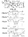
- FIG. 2 represents diagrams of the waveforms at different points of the circuit.
- the curves A, B, C represent the voltages respectively at the terminals of the switches 10 and 3 and at point 19 of the diagram of FIG. 1.
- the curves D and E the intensity of the currents respectively in the switches 10 and 3 (positive for the thyristors 11 and 4 and negative for diodes 12 and 5).
- the instant t is taken at the moment of the reversal of the direction of the current in the scanning inductor 1, that is to say at the moment when the thyristor 4 begins to drive.
- the thyristor 11 is started, the voltage at its terminals becomes zero, and the reactive circuit 8, 9 closes through the two switch devices 10 and 3.
- the oscillating current flowing in the reactive network 8, 9 to through the closed switch 10 is superimposed in the thyristor 4 on the current flowing through the scanning inductance 1.
- the voltage at point 19 passes at time t 2 through zero to then become negative, then it rises according to the period of oscillation of the oscillating circuit constituted by the reactive circuit 8, 9, the scanning inductance 1, and the device 10 But the maximum relative value of this voltage V 19 will not reach at the instant t 4 the initial value that it had before the ignition of the thyristor 11.
- the voltage at point 19 does not resume its initial value until after a second oscillation of an oscillating circuit then formed by the reactive circuit 8, 9 and the scanning inductance 1, the current then passing through the diode 12 by blocking the thyristor 11.
- the thyristor 4 is biased in reverse from the instant t 2 , but it is again subjected to a direct tension from the instant t 3 .
- circuit 8, 9 are chosen so that this time t 3 - t 2 is greater than the recovery time of thyristor 4.
- the negative bias of the trigger of thyristor 4 must begin before time t 2 and continue until at time t 5 at least.
- the voltage V 19 at point 19 of the diagram in FIG. 1 can advantageously be used to develop the drive signal for the trigger of the thyristor 4 provided that the positive peak is eliminated in the interval t 5 - t 3 1 where its anode is positive.
- This voltage V 19 is indeed positive from t 6 to t 2 + T H (where T H is a line period) and negative from t 2 to t 6 .
- T H is a line period
- the driving device therefore comprises a capacitive divider constituted by two capacitors 21 and 22 connected in series between point 19 and earth, through a damping network 17 and 18, and whose output terminal 26 located at the intermediate point between capacitors 21 and 22 is connected to the trigger of thyristor 4 through l inductance 23 and resistor 24, connected in series.
- the value of the capacitors 21 and 22 is chosen so as to lower the voltage at point 26 to a value compatible with the control of the thyristor.
- the function of the inductance 23 and resistance 24 network is to phase-shift the divided voltage waveform V 19 so as to place the peak of the trigger current at the most favorable instant, that is to say approximately at the 'instant t.
- the damping network cons-0 formed by the inductor 17 in parallel with the resistor 18 does not directly intervene in the operation of the trigger drive circuit, but it is necessary to limit the rise of the current at the same time in the capacitive network 9 and the capacitive divider 21, 22.
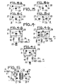
- FIGs 3a, 3b, 3c and 3d give diagrams of different known configurations of the capacitive network 9.
- a single capacitor 31 connects the terminals 27 and 28 of the network, while a capacitor 32 connects the terminal 29 (called ground) to a pole of the capacitor 31.
- the terminals 27 and 28 of the T-shaped network 9 are connected by two capacitors 33 and 34 in series, while terminal 29 is connected by a capacitor 32 to the common pole of capacitors 33 and 34.
- terminals 27 and 28 are joined together by a single capacitor 31, each of the poles of which is connected to terminal 29 by a capacitor respectively 36 and 37, forming a network 9 in ⁇ .
- FIG. 4a represents an assembly of the thyristor drive circuit 4 according to the invention, and adapted to the capacitive network 9 of FIG. 3b, remarkable by the presence of a single capacitor 31 between the terminals 27 and 28 of the capacitive network 9, and a single capacitor 32 between a pole of the capacitor and the terminal 29 connected to ground by the damping network 17 and 18.
- the capacitor 32 of the capacitive network 9 also plays the role of the capacitor 21 of the capacitive divider 21-22 of FIG. 1 and that the capacitor 22 is inserted between the damping network joined to terminal 29 and the mass.
- FIG. 4b represents an assembly of the driving circuit adapted to the configuration in ⁇ of the capacitive network illustrated in FIG. 3d.
- the capacitor 36 is replaced by the two capacitors 21 and 22 of the capacitive divider of FIG. 1.
- FIG. 4c represents another embodiment adapted to the T-shaped assembly of the capacitive network 9 illustrated in FIG. 3c, comprising two capacitors 33 and 34 in series between the inputs 27 and 28.
- the capacitor 32 of the capacitive network 9 is also used as the first capacitor of the capacitive divider (21, figure 1).
- This simplified assembly has however a slight drawback which is constituted by the fact that the presence of the capacitor 33 in this configuration has the effect of increasing the rise in voltage, at time t 4 (curve C in FIG. 2) at the junction. capacitors 33, 34 and 32 and also across capacitor 22. Now we saw above that it was necessary to avoid a positive rise in this voltage at this time. This constraint therefore requires that the capacitor 33 has a much higher capacity than that of the capacitor 34.
- the circuit according to the invention is also of great interest in the case where, in the scanning circuit, the inductor 8 (FIG. 1) is replaced by a transformer.
- the main purpose of this arrangement is to galvanically isolate most of the circuit from the source 6. It can be seen that in the case of such an assembly, it would be contrary to the desired aim to connect, by the drive circuit of the trigger of the scanning thyristor 4, the part of the circuit, which we set out to make "cold", at the "hot” part located between the transformer replacing the inductor 8, and the source 6.
- FIG. 5 represents the partial diagram of a sweeping circuit comprising an isolation transformer 38 in place of the inductor 8.
- This figure shows, in particular the transformer 38, the capacitors 52, 53 and 54 equivalent to capacitors 32, 33 and 34 of the capacitive network 9, which are dispersed, and the output 26 for controlling the trigger of the thyristor 4, the rest of the scanning circuit being the same as that shown in FIG. 1.
- the capacitor 53 is connected here at series with the primary winding of the transformer 38, between one of its terminals and the second switch 10, the other terminal of the primary being connected, with the cathode of the second thyristor 11 and the anode of the second diode 12, to the hot mass C constituted by the negative pole of the source 6.
- the capacitor 54 is connected to one of the terminals of the secondary winding of the transformer 38, the other terminal of which is connected to the cold mass F of the television receiver, which is isolated from the mains .
- the three The fifth capacitor 52 of the capacitive network is connected in series with the second capacitor 22 of the capacitive divider and the resulting series assembly is connected to the terminals of the secondary winding. It can be seen that, as in the case of the capacitor 32 of FIG. 4c, the capacitor 52 is also used as the first capacitor 21 of the capacitive divider (FIG. 1) composed here of the capacitors 22 and 52 whose common point 26 is connected to the circuit of thyristor trigger 4.
Applications Claiming Priority (2)
| Application Number | Priority Date | Filing Date | Title |
|---|---|---|---|
| FR7900420A FR2446572A1 (fr) | 1979-01-09 | 1979-01-09 | Circuit de balayage-ligne pour recepteur de television |
| FR7900420 | 1979-01-09 |
Publications (1)
| Publication Number | Publication Date |
|---|---|
| EP0014108A1 true EP0014108A1 (de) | 1980-08-06 |
Family
ID=9220563
Family Applications (1)
| Application Number | Title | Priority Date | Filing Date |
|---|---|---|---|
| EP80400012A Withdrawn EP0014108A1 (de) | 1979-01-09 | 1980-01-04 | Zeilenablenkschaltung für Fernsehempfänger |
Country Status (5)
| Country | Link |
|---|---|
| US (1) | US4309641A (de) |
| EP (1) | EP0014108A1 (de) |
| ES (1) | ES487493A1 (de) |
| FR (1) | FR2446572A1 (de) |
| PL (1) | PL221284A1 (de) |
Families Citing this family (2)
| Publication number | Priority date | Publication date | Assignee | Title |
|---|---|---|---|---|
| GB0611409D0 (en) * | 2006-06-09 | 2006-07-19 | Rolls Royce Plc | An earthing arrangement |
| TWI334258B (en) * | 2006-12-08 | 2010-12-01 | Delta Networks Inc | Homeplug apparatus and surge protecitng circuit thereof |
Citations (3)
| Publication number | Priority date | Publication date | Assignee | Title |
|---|---|---|---|---|
| DE2524082A1 (de) * | 1975-05-30 | 1976-12-09 | Philips Patentverwaltung | Saegezahn-schaltung |
| FR2313830A1 (fr) * | 1975-06-05 | 1976-12-31 | Int Standard Electric Corp | Circuit d'alimentation pour recepteur de television |
| FR2324167A1 (fr) * | 1975-09-12 | 1977-04-08 | Rca Corp | Circuit de commande de gachette pour un systeme de deviation a thyristors |
Family Cites Families (5)
| Publication number | Priority date | Publication date | Assignee | Title |
|---|---|---|---|---|
| FR1536025A (fr) * | 1966-09-06 | 1968-08-09 | Rca Corp | Circuit de déviation de faisceaux électroniques |
| FR2207354B1 (de) * | 1972-11-22 | 1976-10-29 | Thomson Brandt | |
| GB1545059A (en) * | 1975-05-16 | 1979-05-02 | Rca Corp | Voltage regulator for a television receiver deflection system |
| US4104569A (en) * | 1976-04-26 | 1978-08-01 | Rca Corporation | Horizontal deflection circuit with auxiliary power supply |
| GB1555858A (en) * | 1976-11-23 | 1979-11-14 | Rca Corp | Regulation system for deflection apparatus |
-
1979
- 1979-01-09 FR FR7900420A patent/FR2446572A1/fr not_active Withdrawn
- 1979-12-27 US US06/107,603 patent/US4309641A/en not_active Expired - Lifetime
-
1980
- 1980-01-04 EP EP80400012A patent/EP0014108A1/de not_active Withdrawn
- 1980-01-07 ES ES487493A patent/ES487493A1/es not_active Expired
- 1980-01-09 PL PL22128480A patent/PL221284A1/xx unknown
Patent Citations (3)
| Publication number | Priority date | Publication date | Assignee | Title |
|---|---|---|---|---|
| DE2524082A1 (de) * | 1975-05-30 | 1976-12-09 | Philips Patentverwaltung | Saegezahn-schaltung |
| FR2313830A1 (fr) * | 1975-06-05 | 1976-12-31 | Int Standard Electric Corp | Circuit d'alimentation pour recepteur de television |
| FR2324167A1 (fr) * | 1975-09-12 | 1977-04-08 | Rca Corp | Circuit de commande de gachette pour un systeme de deviation a thyristors |
Also Published As
| Publication number | Publication date |
|---|---|
| ES487493A1 (es) | 1980-06-16 |
| FR2446572A1 (fr) | 1980-08-08 |
| PL221284A1 (de) | 1980-11-03 |
| US4309641A (en) | 1982-01-05 |
Similar Documents
| Publication | Publication Date | Title |
|---|---|---|
| EP0502067B1 (de) | Ladevorrichtung zur elektrischen energiespeicherung mit ladesteuerungsmitteln | |
| EP0680245A2 (de) | Statischer Wandler mit gesteuertem Schalter und Steuerungsschaltung | |
| CA2315893C (fr) | Procede de commande d'un convertisseur de tension continu-continu a stockage inductif | |
| EP0008263B1 (de) | Vertikalabtastschaltung im geschalteten Betrieb für Videofrequenzempfänger und eine solche Schaltung enthaltender Empfänger | |
| FR2538039A1 (fr) | Systeme d'allumage a decharge de condensateur et a etincelles multiples | |
| EP0005391B1 (de) | Einrichtung zur Stabilisierung der Betriebsspannung einer Zeilenablenkschaltung in einem Fernsehempfänger | |
| EP0022380B1 (de) | Mit einer Zeilenablenkschaltung eines Fernsehempfängers kombinierter Sperrwandler zur Erzeugung einer Betriebsspannung, der mittels variabler Phasenverschiebung geregelt wird | |
| EP0043761B1 (de) | Schalttransistorsteuerschaltung in einem statischen Wandler und Wandler mit dieser Schaltung | |
| FR2658674A1 (fr) | Convertisseur continu-continu a commutation a tension nulle. | |
| EP0788219B1 (de) | Steuervorrichtung für eine ZVS-Schaltung | |
| EP0014108A1 (de) | Zeilenablenkschaltung für Fernsehempfänger | |
| EP0430765B1 (de) | Impuls-Stromversorgungssystem für eine Last, mit Mitteln um die durch die Last möglicherweise reflektierte Energie abzuleiten | |
| EP0063974B1 (de) | Schaltungsanordnung einer geregelten Wechselspannungsquelle zur Leistungsstromversorgung aus einer netzartigen Wechselstromquelle | |
| EP0196960A1 (de) | Steuereinrichtung für schnell zu betätigende elektromagnetische Anordnungen | |
| EP0007866B1 (de) | Stabilisierte Speisungsschaltung für einen Videofrequenz-Empfänger und eine solche Schaltung enthaltender Empfänger | |
| FR2471103A1 (fr) | Circuit d'alimentation en courant de deviation et en energie | |
| FR2535551A1 (fr) | Dispositif de commutation electronique a faible dissipation de puissance | |
| EP0424280B1 (de) | Elektronische Ansteuerungsschaltung für einen gleichstromgespeisten Schwingmotor | |
| FR2520958A1 (fr) | Circuit auxiliaire pour televiseur | |
| EP0147306A2 (de) | Linearer Leistungsverstärker | |
| EP0030191A1 (de) | Betriebs-Gleichspannungsgenerator und Fernsehempfänger mit einem solchen Generator | |
| EP0261018B1 (de) | Spannungsfrequenzselbstgeführter Konverter | |
| FR2579039A1 (fr) | Dispositif d'aide a la commutation d'interrupteur et de diode de roue libre | |
| FR2487139A1 (fr) | Circuit hacheur a commutation libre | |
| FR2733648A1 (fr) | Relais statique protege |
Legal Events
| Date | Code | Title | Description |
|---|---|---|---|
| PUAI | Public reference made under article 153(3) epc to a published international application that has entered the european phase |
Free format text: ORIGINAL CODE: 0009012 |
|
| AK | Designated contracting states |
Designated state(s): CH DE GB IT |
|
| 17P | Request for examination filed | ||
| STAA | Information on the status of an ep patent application or granted ep patent |
Free format text: STATUS: THE APPLICATION IS DEEMED TO BE WITHDRAWN |
|
| 18D | Application deemed to be withdrawn |
Effective date: 19820706 |
|
| RIN1 | Information on inventor provided before grant (corrected) |
Inventor name: SHEPERD, JOHN |