EP2806549A1 - Steuerverfahren für Stromwandler - Google Patents
Steuerverfahren für Stromwandler Download PDFInfo
- Publication number
- EP2806549A1 EP2806549A1 EP13168560.4A EP13168560A EP2806549A1 EP 2806549 A1 EP2806549 A1 EP 2806549A1 EP 13168560 A EP13168560 A EP 13168560A EP 2806549 A1 EP2806549 A1 EP 2806549A1
- Authority
- EP
- European Patent Office
- Prior art keywords
- link voltage
- link
- voltage
- inverter
- maximum
- Prior art date
- Legal status (The legal status is an assumption and is not a legal conclusion. Google has not performed a legal analysis and makes no representation as to the accuracy of the status listed.)
- Withdrawn
Links
Images
Classifications
-
- H—ELECTRICITY
- H02—GENERATION; CONVERSION OR DISTRIBUTION OF ELECTRIC POWER
- H02M—APPARATUS FOR CONVERSION BETWEEN AC AND AC, BETWEEN AC AND DC, OR BETWEEN DC AND DC, AND FOR USE WITH MAINS OR SIMILAR POWER SUPPLY SYSTEMS; CONVERSION OF DC OR AC INPUT POWER INTO SURGE OUTPUT POWER; CONTROL OR REGULATION THEREOF
- H02M1/00—Details of apparatus for conversion
- H02M1/14—Arrangements for reducing ripples from dc input or output
- H02M1/15—Arrangements for reducing ripples from dc input or output using active elements
-
- H—ELECTRICITY
- H02—GENERATION; CONVERSION OR DISTRIBUTION OF ELECTRIC POWER
- H02M—APPARATUS FOR CONVERSION BETWEEN AC AND AC, BETWEEN AC AND DC, OR BETWEEN DC AND DC, AND FOR USE WITH MAINS OR SIMILAR POWER SUPPLY SYSTEMS; CONVERSION OF DC OR AC INPUT POWER INTO SURGE OUTPUT POWER; CONTROL OR REGULATION THEREOF
- H02M3/00—Conversion of dc power input into dc power output
- H02M3/02—Conversion of dc power input into dc power output without intermediate conversion into ac
- H02M3/04—Conversion of dc power input into dc power output without intermediate conversion into ac by static converters
- H02M3/10—Conversion of dc power input into dc power output without intermediate conversion into ac by static converters using discharge tubes with control electrode or semiconductor devices with control electrode
- H02M3/145—Conversion of dc power input into dc power output without intermediate conversion into ac by static converters using discharge tubes with control electrode or semiconductor devices with control electrode using devices of a triode or transistor type requiring continuous application of a control signal
- H02M3/155—Conversion of dc power input into dc power output without intermediate conversion into ac by static converters using discharge tubes with control electrode or semiconductor devices with control electrode using devices of a triode or transistor type requiring continuous application of a control signal using semiconductor devices only
- H02M3/156—Conversion of dc power input into dc power output without intermediate conversion into ac by static converters using discharge tubes with control electrode or semiconductor devices with control electrode using devices of a triode or transistor type requiring continuous application of a control signal using semiconductor devices only with automatic control of output voltage or current, e.g. switching regulators
- H02M3/158—Conversion of dc power input into dc power output without intermediate conversion into ac by static converters using discharge tubes with control electrode or semiconductor devices with control electrode using devices of a triode or transistor type requiring continuous application of a control signal using semiconductor devices only with automatic control of output voltage or current, e.g. switching regulators including plural semiconductor devices as final control devices for a single load
- H02M3/1584—Conversion of dc power input into dc power output without intermediate conversion into ac by static converters using discharge tubes with control electrode or semiconductor devices with control electrode using devices of a triode or transistor type requiring continuous application of a control signal using semiconductor devices only with automatic control of output voltage or current, e.g. switching regulators including plural semiconductor devices as final control devices for a single load with a plurality of power processing stages connected in parallel
- H02M3/1586—Conversion of dc power input into dc power output without intermediate conversion into ac by static converters using discharge tubes with control electrode or semiconductor devices with control electrode using devices of a triode or transistor type requiring continuous application of a control signal using semiconductor devices only with automatic control of output voltage or current, e.g. switching regulators including plural semiconductor devices as final control devices for a single load with a plurality of power processing stages connected in parallel switched with a phase shift, i.e. interleaved
Definitions
- the present invention relates to control methods for power converters, and in particular to control methods that minimise current ripple.
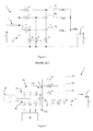
- Figure 1 shows an N -phase interleaved bi-directional buck converter (or step-down converter) topology.
- a converter 1 consists of N converter circuits connected in parallel between a dc link 2 and a dc load/source 4.
- Each converter circuit has a synchronous topology with a first switch 6 1 , 6 2 ...6 N , a second switch 8 1 , 8 2 ...8 N and a reactor (or inductor) 10 1 , 10 2 ...10 N .
- a first converter circuit (or 'phase') of the buck converter 1 includes a first switch 6 1 , a second switch 8 1 and a reactor 10 1 ;
- a second converter circuit includes a first switch 6 2 , a second switch 8 2 and a reactor 10 2 ; and so on for each converter circuit.
- a capacitor 12 is connected across the dc link 2.
- the buck converter is bi-directional, power can flow from the dc link 2 to the dc load/source 4 and power can flow from the dc load/source 4 to the dc link 2 depending on operational requirements.
- the switching strategies of the individual converter circuits are interleaved.
- a higher duty ratio can be defined by: a - 1 N ⁇ D ⁇ a N where a is a positive integer less than N.
- a converter circuits can be 'on' (or charging) at any particular time and ( N - a ) converter circuits can be 'off' (or discharging).
- the present invention provides a method of operating a power converter arrangement comprising: a dc link; a dc load/source; an active rectifier/inverter having dc terminals connected to the dc link and adapted to provide a variable dc link voltage ( V 1 ) between maximum and minimum limits ( V 1,max , V 1,min ); and an interleaved buck (or step-down) converter having N converter circuits connected between the dc link and the dc load/source, each converter circuit including a first switch, a second switch and a reactor; the method comprising the steps of:
- the active rectifier/inverter is controlled to provide a dc link voltage that is substantially the same as a null value of dc link voltage then there will be substantially no ripple on the converter current, i.e., the current experienced by the dc load/source will be substantially ripple-free.
- the active rectifier/inverter is normally controlled to provide a substantially constant dc link voltage.
- the dc link voltage can be varied deliberately (e.g., by a controller for the active rectifier/inverter) in response to changes in the voltage V 2 across the dc load/source in order to try and minimise current ripple.
- the active rectifier/inverter can be controlled to provide a dc link voltage that is substantially the same as any of the null values.
- the highest null value will typically be selected because this lowers the dc link current and reduces losses in the power converter arrangement.
- the method may further comprise the step of controlling the active rectifier/inverter to provide a dc link voltage that is substantially the same as the maximum or minimum limit of the dc link voltage.
- the active rectifier/inverter controls the active rectifier/inverter to provide a dc link voltage that is substantially the same as the maximum or minimum limit reduces the current ripple as much as possible while still keeping the dc link voltage within its practical and operational constraints.
- the selection between the maximum or minimum limit can be based on whichever is closer to a null value and hence will provide the least current ripple.
- the active rectifier/inverter can be controlled to provide a dc link voltage that is substantially the same as whichever of the maximum and minimum limit will provide the least current ripple for the prevailing voltage V 2 .
- the maximum limit can also be selected in preference to the minimum limit because this lowers the dc link current and reduces losses in the power converter arrangement.
- the present invention further provides a power converter arrangement comprising: a dc link; a dc load/source; an active rectifier/inverter having dc terminals connected to the dc link and adapted to provide a variable dc link voltage between maximum and minimum limits; an interleaved buck (or step-down) converter having N converter circuits connected between the dc link and the dc load/source, each converter circuit including a first switch, a second switch and a reactor; and a controller for the active rectifier/inverter adapted to implement the method described above.
- the active rectifier/inverter can have any suitable topology and include any suitable power semiconductor switching devices, optionally controlled using a pulse width modulation (PWM) strategy.
- PWM pulse width modulation
- the active rectifier/inverter can have a two- or three-level topology as appropriate.
- FIG 2 shows a power converter arrangement according to the present invention where an N -phase interleaved bi-directional buck converter 1 is combined with an AC/DC converter, e.g., an active rectifier/inverter 20.
- the buck converter 1 is generally as described above with reference to Figure 1 and like parts have been given the same reference numeral.
- a smoothing capacitor 14 is connected in parallel across the dc load/source 4.
- the buck converter 1 operates as a DC/DC converter.
- the active rectifier/inverter 20 includes a plurality of switches 22 that are typically controlled to open and close in accordance with a pulse width modulation (PWM) strategy.
- the active rectifier/inverter 20 is controlled by a controller 30 which provides gate command signals for opening and closing the switches 22.
- the active rectifier/inverter 20 includes dc terminals 24a, 24b that are connected to the dc link 2 of the buck converter 1 and ac terminals 26 that are connected to an ac network or grid 28. Power can be supplied from the ac network 28 to the dc load/source 4 to charge the dc load/source and in this case the active rectifier/inverter 20 will operate as an active rectifier. Power can be discharged from the dc load/source 4 to the ac network 28 and in this case the active rectifier/inverter 20 will operate as an inverter.
- the active rectifier/inverter 20 can be operated to control the dc link voltage V 1 .
- the applicant has found that the dc link voltage V 1 can be varied deliberately by the controller 30 with reference to the voltage V 2 in order to minimise the ripple on the converter current I .
- null values can also be considered in terms of null values of the duty cycle D of the buck converter 1.
- the null values of dc link voltage can be determined (e.g., by the controller 30) for each value of a and with reference to the prevailing voltage V 2 as shown in equation EQ16.
- the active rectifier/inverter 20 can then be controlled to provide a dc link voltage V 1 that is substantially the same as a null value.
- the active rectifier/inverter 20 can be controlled in this manner irrespective of whether it is operating as an active rectifier or an inverter.
- the buck converter 1 is controlled in a conventional manner to supply power from the dc link 2 to the dc load/source 4 or to supply power from the dc load/source to the dc link depending on whether the dc load/source 4 is being charged or discharged.
- the dc link voltage V 1 will often be constrained to be within maximum and minimum limits. If there is no null value within the maximum and minimum limits then the ripple current cannot be substantially eliminated, but merely minimised as far as possible by controlling the active rectifier/inverter 20 to provide a dc link voltage V 1 that is substantially the same as one of the maximum and minimum limits, typically the limit that is closest to a null value of the dc link voltage or which minimises losses in the power converter arrangement. It will be understood that this still provides a useful improvement over the conventional power converter arrangement where the dc link voltage V 1 remains substantially constant.
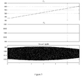
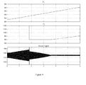
- Figures 3 and 4 show simulated results for the power converter arrangement of Figure 2 .
- the power converter arrangement is controlled according to the method of the present invention such that the dc link voltage V 1 is varied deliberately to minimise current ripple.
- the upper plot of Figures 3 and 4 illustrates a situation where the voltage V 2 across the dc load/source 4 increases at a constant rate from 430 V to 600 V.
- the lower plot of Figures 3 and 4 illustrates current ripple.
- the dc link voltage V 1 cannot be set to either of these null values because they are both outside the maximum and minimum limits.
- the active rectifier/inverter 20 is therefore controlled to provide a dc link voltage V 1 at the maximum limit of 1200 V.
- the dc link voltage V 1 remains constant at the maximum limit of 1200 V and the current ripple gradually increases as the voltage V 2 increases. This is because the dc link voltage V 1 gradually gets further away from the upper null value for the prevailing voltage V 2 .
- the active rectifier/inverter 20 is therefore controlled to switch the dc link voltage V 1 from the maximum limit of 1200 V to the minimum level of 800 V.
- the active rectifier/inverter 20 is controlled to maintain the dc link voltage V 1 constant at the minimum limit of 800 V and the current ripple gradually decreases as the voltage V 2 increases. This is because the dc link voltage V 1 gradually gets closer to the lower null value for the prevailing voltage V 2 .
- the upper null value of 1599 V is still outside the maximum and minimum limits.
- the lower null value of 800 V is at the minimum limit for the dc link voltage V 1 .
- the current ripple illustrated in Figure 4 simulates a power converter arrangement where the reactors 10 1 , 10 2 and 10 3 of the buck converter 1 have ideal characteristics. However, the reactors will have stray (or parasitic) resistances that can have an affect on the current ripple that can actually be achieved in practice.
Landscapes
- Engineering & Computer Science (AREA)
- Power Engineering (AREA)
- Dc-Dc Converters (AREA)
Priority Applications (6)
| Application Number | Priority Date | Filing Date | Title |
|---|---|---|---|
| EP13168560.4A EP2806549A1 (de) | 2013-05-21 | 2013-05-21 | Steuerverfahren für Stromwandler |
| CA2851931A CA2851931A1 (en) | 2013-05-21 | 2014-05-15 | Control methods for power converters |
| IN2465CH2014 IN2014CH02465A (de) | 2013-05-21 | 2014-05-19 | |
| BRBR102014012240-0A BR102014012240A2 (pt) | 2013-05-21 | 2014-05-21 | Método de operação de um arranjo de conversor de energia e arranjo de conversor de energia |
| US14/283,710 US20140347899A1 (en) | 2013-05-21 | 2014-05-21 | Control methods for power converters |
| CN201410216365.8A CN104184330A (zh) | 2013-05-21 | 2014-05-21 | 功率变换器控制方法 |
Applications Claiming Priority (1)
| Application Number | Priority Date | Filing Date | Title |
|---|---|---|---|
| EP13168560.4A EP2806549A1 (de) | 2013-05-21 | 2013-05-21 | Steuerverfahren für Stromwandler |
Publications (1)
| Publication Number | Publication Date |
|---|---|
| EP2806549A1 true EP2806549A1 (de) | 2014-11-26 |
Family
ID=48444247
Family Applications (1)
| Application Number | Title | Priority Date | Filing Date |
|---|---|---|---|
| EP13168560.4A Withdrawn EP2806549A1 (de) | 2013-05-21 | 2013-05-21 | Steuerverfahren für Stromwandler |
Country Status (6)
| Country | Link |
|---|---|
| US (1) | US20140347899A1 (de) |
| EP (1) | EP2806549A1 (de) |
| CN (1) | CN104184330A (de) |
| BR (1) | BR102014012240A2 (de) |
| CA (1) | CA2851931A1 (de) |
| IN (1) | IN2014CH02465A (de) |
Families Citing this family (1)
| Publication number | Priority date | Publication date | Assignee | Title |
|---|---|---|---|---|
| US9748847B2 (en) | 2014-10-23 | 2017-08-29 | Qualcomm Incorporated | Circuits and methods providing high efficiency over a wide range of load values |
Citations (3)
| Publication number | Priority date | Publication date | Assignee | Title |
|---|---|---|---|---|
| FR2790616A1 (fr) * | 1999-03-05 | 2000-09-08 | Sagem | Circuit changeur de tension a decoupages decales et reseau de distribution d'energie en faisant application |
| US20040070283A1 (en) * | 2002-10-09 | 2004-04-15 | Robert Maple | Duty cycle phase number control of polyphase interleaved converters |
| EP1536549A2 (de) * | 2003-11-28 | 2005-06-01 | Kabushiki Kaisha Toshiba | Stromversorgungsvorrichtung |
Family Cites Families (7)
| Publication number | Priority date | Publication date | Assignee | Title |
|---|---|---|---|---|
| US4270078A (en) * | 1979-04-24 | 1981-05-26 | General Electric Company | Method and apparatus for a variable frequency inverter system having commutation fault detection and correction capabilities |
| JPH074067B2 (ja) * | 1986-01-24 | 1995-01-18 | 株式会社明電舍 | 電流形gtoインバ−タの無効電力処理回路 |
| US5198970A (en) * | 1988-04-27 | 1993-03-30 | Mitsubishi Denki Kabushiki Kaisha | A.C. power supply apparatus |
| FR2633115B1 (fr) * | 1988-06-17 | 1993-02-12 | Gen Electric Cgr | Alimentation stabilisee a taux d'ondulation reduit |
| DE69025045T2 (de) * | 1989-12-04 | 1996-05-30 | Toshiba Kawasaki Kk | Leistungswandler vom Brückentyp mit verbessertem Wirkungsgrad |
| JP2006074965A (ja) * | 2004-09-06 | 2006-03-16 | Honda Motor Co Ltd | 電源装置 |
| US9042131B2 (en) * | 2013-02-15 | 2015-05-26 | Ideal Power Inc. | Power-packet-switching converter with sequenced connection to link inductor |
-
2013
- 2013-05-21 EP EP13168560.4A patent/EP2806549A1/de not_active Withdrawn
-
2014
- 2014-05-15 CA CA2851931A patent/CA2851931A1/en not_active Abandoned
- 2014-05-19 IN IN2465CH2014 patent/IN2014CH02465A/en unknown
- 2014-05-21 US US14/283,710 patent/US20140347899A1/en not_active Abandoned
- 2014-05-21 BR BRBR102014012240-0A patent/BR102014012240A2/pt not_active Application Discontinuation
- 2014-05-21 CN CN201410216365.8A patent/CN104184330A/zh active Pending
Patent Citations (3)
| Publication number | Priority date | Publication date | Assignee | Title |
|---|---|---|---|---|
| FR2790616A1 (fr) * | 1999-03-05 | 2000-09-08 | Sagem | Circuit changeur de tension a decoupages decales et reseau de distribution d'energie en faisant application |
| US20040070283A1 (en) * | 2002-10-09 | 2004-04-15 | Robert Maple | Duty cycle phase number control of polyphase interleaved converters |
| EP1536549A2 (de) * | 2003-11-28 | 2005-06-01 | Kabushiki Kaisha Toshiba | Stromversorgungsvorrichtung |
Also Published As
| Publication number | Publication date |
|---|---|
| BR102014012240A2 (pt) | 2015-05-26 |
| CN104184330A (zh) | 2014-12-03 |
| US20140347899A1 (en) | 2014-11-27 |
| CA2851931A1 (en) | 2014-11-21 |
| IN2014CH02465A (de) | 2015-07-03 |
Similar Documents
| Publication | Publication Date | Title |
|---|---|---|
| CN104242651B (zh) | 用于多相转换器的高级相数控制 | |
| CN102132478B (zh) | 具有动态阈值的磁滞降压变换器 | |
| EP2963798B1 (de) | Dc-ac-umwandlungsvorrichtung und steuerschaltung | |
| US20090237016A1 (en) | Motor controller | |
| EP2858225A1 (de) | Stromwandlervorrichtung | |
| CN103683918A (zh) | 开关电源装置 | |
| JP2010239770A (ja) | Dc/dcコンバータおよびそれを用いた給電システム | |
| US20180062498A1 (en) | Power conversion device | |
| CN106464150B (zh) | 电力转换装置 | |
| CN107370389B (zh) | 用于克服异常电网状况的电力转换系统及其操作方法 | |
| US8830701B2 (en) | DC-DC converter | |
| CN104704732A (zh) | 用于调节电流源的方法以及用于此的电流源和过程调节器 | |
| CN103427701A (zh) | 用于运行变流器的方法和变流器控制单元 | |
| JP7001896B2 (ja) | Dc-dcコンバータ | |
| CN104362720B (zh) | 一种蓄电池充电系统 | |
| US20100007211A1 (en) | Control device and control method for power conversion system having instantaneous voltage drop - service interruption counter-measure functions | |
| EP3391543B1 (de) | Spannungsausgleich von spannungsquellenwandlern | |
| EP2806549A1 (de) | Steuerverfahren für Stromwandler | |
| CN102969909B (zh) | 具有可开关pfc的ac/dc转换器及其控制器和操作控制器的方法 | |
| CN104362717B (zh) | 一种蓄电池充电系统 | |
| CN101599692B (zh) | 切换式电源转换器的快速响应装置及方法 | |
| CN110289639B (zh) | 一种级联式变流器及其控制方法和应用系统 | |
| CN113746170A (zh) | 一种储能系统及其离网过载保护方法 | |
| CN102801383A (zh) | 具有充电功能的交流电动机驱动装置及其充电方法 | |
| US20220239146A1 (en) | Power supply device |
Legal Events
| Date | Code | Title | Description |
|---|---|---|---|
| PUAI | Public reference made under article 153(3) epc to a published international application that has entered the european phase |
Free format text: ORIGINAL CODE: 0009012 |
|
| 17P | Request for examination filed |
Effective date: 20130521 |
|
| AK | Designated contracting states |
Kind code of ref document: A1 Designated state(s): AL AT BE BG CH CY CZ DE DK EE ES FI FR GB GR HR HU IE IS IT LI LT LU LV MC MK MT NL NO PL PT RO RS SE SI SK SM TR |
|
| AX | Request for extension of the european patent |
Extension state: BA ME |
|
| R17P | Request for examination filed (corrected) |
Effective date: 20150513 |
|
| RBV | Designated contracting states (corrected) |
Designated state(s): AL AT BE BG CH CY CZ DE DK EE ES FI FR GB GR HR HU IE IS IT LI LT LU LV MC MK MT NL NO PL PT RO RS SE SI SK SM TR |
|
| STAA | Information on the status of an ep patent application or granted ep patent |
Free format text: STATUS: THE APPLICATION IS DEEMED TO BE WITHDRAWN |
|
| 18D | Application deemed to be withdrawn |
Effective date: 20150527 |