EP0346777A1 - Schaltung zur Kodierung eines dreiteiligen Kodes - Google Patents
Schaltung zur Kodierung eines dreiteiligen Kodes Download PDFInfo
- Publication number
- EP0346777A1 EP0346777A1 EP89110496A EP89110496A EP0346777A1 EP 0346777 A1 EP0346777 A1 EP 0346777A1 EP 89110496 A EP89110496 A EP 89110496A EP 89110496 A EP89110496 A EP 89110496A EP 0346777 A1 EP0346777 A1 EP 0346777A1
- Authority
- EP
- European Patent Office
- Prior art keywords
- data
- clock
- time
- transition
- bit
- Prior art date
- Legal status (The legal status is an assumption and is not a legal conclusion. Google has not performed a legal analysis and makes no representation as to the accuracy of the status listed.)
- Withdrawn
Links
Images

Classifications
-
- G—PHYSICS
- G11—INFORMATION STORAGE
- G11B—INFORMATION STORAGE BASED ON RELATIVE MOVEMENT BETWEEN RECORD CARRIER AND TRANSDUCER
- G11B20/00—Signal processing not specific to the method of recording or reproducing; Circuits therefor
- G11B20/10—Digital recording or reproducing
- G11B20/14—Digital recording or reproducing using self-clocking codes
-
- H—ELECTRICITY
- H03—ELECTRONIC CIRCUITRY
- H03M—CODING; DECODING; CODE CONVERSION IN GENERAL
- H03M5/00—Conversion of the form of the representation of individual digits
- H03M5/02—Conversion to or from representation by pulses
- H03M5/04—Conversion to or from representation by pulses the pulses having two levels
- H03M5/06—Code representation, e.g. transition, for a given bit cell depending only on the information in that bit cell
- H03M5/12—Biphase level code, e.g. split phase code, Manchester code; Biphase space or mark code, e.g. double frequency code
Definitions
- This invention relates to electrical circuits suitable for encoding a binary data stream into a three-part code format.
- a novel method for modulating a binary data stream into a code format suitable for encoding and decoding e.g., magnetic information or optical information, is disclosed in the above-cited Application Ser. No. 206,646 to Wash.
- the novel method features self-clocking, velocity insensitive encoding and decoding.
- the Wash disclosure states that preferred electrical circuits that may be employed for realizing the encoding scheme set forth in that disclosure are provided in the present application.
- This application therefore, provides novel electrical circuits that may be advantageously employed, for example, for encoding a binary data stream into a three-part code format in accordance with the Wash disclosure.
- the novel electrical circuits encode the data and preserve the self-clocking, velocity insensitive features of the novel method.
- the invention provides an electrical circuit suitable for encoding a three-part code format from a binary data stream, which circuit comprises:
- the clock means comprises:
- the clock means comprises:
- the serial data encoder preferably comprises:
- the invention provides an electrical circuit suitable for encoding a three-part code format from a binary data stream, which circuit comprises:
- the ratio encodes a data 0 bit, and the ratio encodes a data 1 bit.
- the clock transitions are the opposite polarity of the data transition.
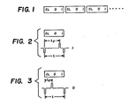
- FIG. 1 reproduces the Wash FIG. 1 three-part code format comprising a [Clock(CL) 0 1] sequence.
- the sequence denotes time locations for logic transitions.
- a term "transition pulse” usually refers to only one edge i.e., either leading (low-to-high) or trailing (high-to-low) of a pulse.
- FIG. 1 three-part code format, in accordance with one aspect of the Wash disclosure, operates on an input binary data stream by the method steps of:
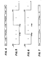
- FIG. 4 shows a three-part code format comprising a [DCL 0 time 1 time] (DCL is an abbreviation of "Data Clock”.) sequence.
- DCL is an abbreviation of "Data Clock”.
- FIG. 5 shows an encoded data 1 bit. The encoding proceeds in accordance with the method steps set forth above.
- a clock transition is written at the beginning or DCL location of the bitcell.
- the logic level goes from high to low.
- the logic level stays low through the location 0 time, and jumps at the data transition to a logic high at the location 1 time.
- the logic level stays high until the adjacent clock transition at the time t, as measured from the previous clock transition.
- a data 1 bit has thus been encoded, since Note that the waveform of FIG. 5 is substantially the same as the waveform for FIG. 2, since both encode a data 1 bit by way of the same method steps.
- FIG. 6 shows a clock transition that is written at the beginning or DCL location of the bitcell, where the logic level goes from high to low. The logic level stays low until the location 0 time, at which point the logic level jumps with the data transition at time t d to a logic high. The logic level stays high until the adjacent clock transition.
- a data 0 bit has thus been encoded, since Note that the waveform of FIG. 6 is substantially the same as the waveform for FIG. 3, since both encode a data 0 bit by way of the same method steps.
- an intermediate low-to-high data transition occurs between two adjacent and successive clock transitions (high-to-low), near one of two predetermined locations, 0 time or 1 time, depending on whether the current data bit to be encoded is a data 0 bit or data 1 bit, respectively.
- FIG. 7 shows a [DCL D 1] sequence.
- the FIG. 7 format may first be distinguished from the FIG. 4 format, in that the "1 time" location of FIG.
- FIG. 7 format replaces the FIG. 4 "0 time” enumeration, by a corresponding D enumeration.
- D signifies the logic transformation, "NOT Data”.
- NOT Data the logic transformation
- a data 1 bit becomes, under the D transformation, a logic low at "0 time”
- a data 0 bit becomes, under the D transformation, a logic high at "0 time”.
- FIG. 8 shows an electrical circuit 10 suitable for encoding a three-part code format from a binary data stream.
- the circuit 10 comprises a three-phase clock circuit 12, and a data encoder 14.
- the clock circuit 12 comprises a modulo-3 counter 16, a 2-3 demultiplexer-decoder 18, and an inverter 20.
- the clock circuit 12 is structurally completed by observing that the modulo-3 counter 16 accepts outside clock pulses from an outside clock 22, along a line 24.
- the modulo-3 counter 16 provides outputs along lines 26, 28 to the decoder 18, and receives an input along a line 30 which is an output from the decoder 18.
- the decoder 18 provides a set of three output information signals, namely [D clock 0 time 1 time] for input, along three lines 32, 34, 38 respectively, to the data encoder 14.
- the data encoder 14 accepts binary data from an outside line 40.
- the binary data is routed through an inverter 42, an AND gate 44, an OR gate 46 and a flip-flop 48.
- the connecting lines 50, 52, 54 and 56 provide the appropriate routing paths.
- the data encoder 14 also includes an inverter 58 which accepts from the clock circuit 12 the 1 time information from line 38, and inputs an inverted 1 time information signal along a line 60 to the OR gate 46.
- the clock circuit 12 generates three one-bit information signals, which signals demarcate the bitcell and demarcate three transition locations within a given bitcell i.e., [DCL 0 time 1 time] per FIGS. 4, 5 or 6 above; the data encoder 14, in coordination with the clock information signals, places the transitions in the proper locations based on the binary data from line 40.
- a data 1 bit is provided along the line 40 for input to the data encoder 14.
- the data 1 bit is first encoded at the location DCL. To do this, the data 1 bit is inverted by the inverter 42, and becomes a data 0 bit i.e., D .
- the data 0 bit, or D in turn, becomes the first of the two inputs to the AND gate 44.
- the second input to the AND gate 44 is the inverted 0 time logic level on line 36, namely, a logic low.
- the AND gate 44 therefore outputs a logic low, given its two logic low inputs. Continuing, the AND gate 44 logic low output becomes the first of two inputs to the OR gate 46.
- the OR gate 46 second input is the inverted 1 time logic level on line 60, namely, a logic low.
- the OR gate 46 accordingly, outputs a logic low, given its two logic low inputs.
- This OR′d logic low output may be stored by the flip-flop 48, and represents the encoded portion of the data 1 bit for the DCL location. This result is in agreement with FIG. 5 above.
- the next location of encoding the data 1 bit occurs at the 0 time location.
- the clock circuit 12 therefore, now outputs a logic high on line 32, a logic low on line 34, and a logic high on line 38.
- the data 1 bit has not changed, however, so that the line 50 input to the AND gate 44, D , is still a logic low.
- the second AND gate 44 input is the inverted 0 time logic, namely, a logic high.
- the logical AND operation determines if a data bit transition is to occur at the 0 time location.
- a data bit 1 should have a logic low. This is in fact what the AND operation provides.
- the AND gate 44 outputs a logic low, given its low and high logic inputs.
- the AND gate 44 logic low output becomes the first of two inputs to the OR gate 46.
- the second OR gate 46 input is the inverted 1 time logic on line 60, namely, a logic low.
- the OR gate 46 accordingly, outputs a logic low, given its two logic low inputs.
- This OR′d logic low output may be stored by the flip-flop 48, and represents the encoded portion of the data bit 1 for the 0 time location. This result is in agreement with FIG. 5 above.
- the AND gate 44 logic low output becomes the first of two inputs to the OR gate 46.
- the OR gate 46 second input is the inverted 1 time logic on line 60, namely, a logic high.
- the logical OR gate 46 operation determines if a data bit transition is to occur at the 1 time location. We know from FIG. 5 above, that at the 1 time location, a data bit 1 should have a logic high. This is in fact what the OR gate 46 provides.
- the OR gate 46 accordingly, outputs a logic high, given its low and high logic inputs.
- This OR′d logic high output may be stored by the flip-flop 48, and represents the encoded portion of the data 1 bit for the 1 time location. This result is in agreement with FIG. 5 above.
- the data bit 1 has now been encoded by the circuit 10 so that it has a complete encoded waveform identical to FIG. 5 above.
- the operation of the circuit 10 for encoding a data 0 bit proceeds mutatis mutandis.
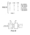
- the clock circuit generates information signals in accordance with Table I.
- D 1 throughout the encoding locations. This difference results in a data 0 bit encoding that is in agreement with FIG. 6 above.
- the clock circuit 12 comprises the modulo-3 counter 16, which accepts clock pulses from the outside clock 22, and the 2-3 demultiplexer-decoder 18.
- the modulo-3 counter 16 receives an outside clock pulse, running at 3 times the frequency of the input data stream, and generates sequentially three binary pairs viz., This sequence of binary pairs, provided in turn as inputs via the line pair 26, 28 to the decoder 18, result in a sequence of binary triplets viz., The decoder 18 output in the FIG.
- this second matrix corresponds to Table I, and represents the information signals.
- a decoder that provides the first sequence may be utilized, thus dispensing with the inverters 20 and 58, and necessitating an inverter (not shown) interrupting line 32.
- the clock circuit 12 operation is completed with the fact that the decoder 18, by way of the 1 time signal on line 30, resets the modulo-3 counter 16, at the end of a bitcell, in anticipation of the start of a new bitcell.
- FIG. 8 electrical circuit 10 The operation of the FIG. 8 electrical circuit 10 is conditioned on the following criteria:
- the three-part code format can also be encoded by a software program running in a microprocessor, thus eliminating the need for discrete hardware.
- One drawback to this, however, is speed, since most microprocessors, without the addition of memory/buffer circuits and output hardware, will not be able to send out the three-part encoded data as fast as, for example, the FIG 8 circuit 10.
- a suitable software encoding routine written in BASIC language is now listed:
Landscapes
- Engineering & Computer Science (AREA)
- Theoretical Computer Science (AREA)
- Signal Processing (AREA)
- Dc Digital Transmission (AREA)
- Compression, Expansion, Code Conversion, And Decoders (AREA)
Applications Claiming Priority (2)
| Application Number | Priority Date | Filing Date | Title |
|---|---|---|---|
| US07/206,408 US4912467A (en) | 1988-06-14 | 1988-06-14 | Three-part encoder circuit |
| US206408 | 1988-06-14 |
Publications (1)
| Publication Number | Publication Date |
|---|---|
| EP0346777A1 true EP0346777A1 (de) | 1989-12-20 |
Family
ID=22766236
Family Applications (1)
| Application Number | Title | Priority Date | Filing Date |
|---|---|---|---|
| EP89110496A Withdrawn EP0346777A1 (de) | 1988-06-14 | 1989-06-09 | Schaltung zur Kodierung eines dreiteiligen Kodes |
Country Status (4)
| Country | Link |
|---|---|
| US (1) | US4912467A (de) |
| EP (1) | EP0346777A1 (de) |
| KR (1) | KR900702529A (de) |
| WO (1) | WO1989012893A1 (de) |
Cited By (2)
| Publication number | Priority date | Publication date | Assignee | Title |
|---|---|---|---|---|
| JPH04156450A (ja) * | 1990-10-19 | 1992-05-28 | Fuji Photo Film Co Ltd | 撮影用写真フィルム処理方法 |
| EP0475447A3 (en) * | 1990-09-14 | 1992-09-23 | Fuji Photo Film Co Ltd | Magnetically recordable photographic film, recording method and system therefor and camera-laboratory system |
Families Citing this family (6)
| Publication number | Priority date | Publication date | Assignee | Title |
|---|---|---|---|---|
| US5115356A (en) * | 1989-08-31 | 1992-05-19 | Eastman Kodak Company | Decoder circuit with missing clock generator |
| US5438461A (en) * | 1991-07-19 | 1995-08-01 | Canon Kabushiki Kaisha | Magnetic reproduction apparatus for a camera |
| US5204708A (en) * | 1991-12-20 | 1993-04-20 | Eastman Kodak Company | Method and apparatus for magnetically communicating via a photographic filmstrip with enhanced reliability |
| US5600499A (en) * | 1993-04-09 | 1997-02-04 | Western Digital Corporation | Tri-bit encoding for disk drive servo track ID information |
| US6493514B1 (en) | 2001-09-04 | 2002-12-10 | Eastman Kodak Company | Method and apparatus for magnetic communication via a photographic filmstrip |
| WO2016084544A1 (ja) * | 2014-11-25 | 2016-06-02 | ソニー株式会社 | 画素ユニット、表示パネル、および信号伝送方法 |
Citations (2)
| Publication number | Priority date | Publication date | Assignee | Title |
|---|---|---|---|---|
| FR2361776A1 (fr) * | 1976-08-09 | 1978-03-10 | Hewlett Packard Co | Appareil decodeur-codeur d'echantillonnage adaptatif et procede de decodage/codage correspondant |
| GB1542398A (en) * | 1976-05-24 | 1979-03-21 | Secr Defence | Recording data |
Family Cites Families (4)
| Publication number | Priority date | Publication date | Assignee | Title |
|---|---|---|---|---|
| US3120927A (en) * | 1963-01-14 | 1964-02-11 | Holland Co J H | Spraybar |
| US4016801A (en) * | 1974-09-30 | 1977-04-12 | Ingersoll-Rand Company | Method for forming threads |
| US4127878A (en) * | 1975-12-24 | 1978-11-28 | Micro Communications Corporation | Magnetic tape recorder/reproducer for ratio recording with synchronized internal and external clock rates |
| US4173026A (en) * | 1978-02-23 | 1979-10-30 | Cubic Western Data | Self clocking speed tolerant magnetic recording method and apparatus |
-
1988
- 1988-06-14 US US07/206,408 patent/US4912467A/en not_active Expired - Fee Related
-
1989
- 1989-06-06 WO PCT/US1989/002447 patent/WO1989012893A1/en not_active Ceased
- 1989-06-06 KR KR1019900700299A patent/KR900702529A/ko not_active Withdrawn
- 1989-06-09 EP EP89110496A patent/EP0346777A1/de not_active Withdrawn
Patent Citations (2)
| Publication number | Priority date | Publication date | Assignee | Title |
|---|---|---|---|---|
| GB1542398A (en) * | 1976-05-24 | 1979-03-21 | Secr Defence | Recording data |
| FR2361776A1 (fr) * | 1976-08-09 | 1978-03-10 | Hewlett Packard Co | Appareil decodeur-codeur d'echantillonnage adaptatif et procede de decodage/codage correspondant |
Cited By (5)
| Publication number | Priority date | Publication date | Assignee | Title |
|---|---|---|---|---|
| EP0475447A3 (en) * | 1990-09-14 | 1992-09-23 | Fuji Photo Film Co Ltd | Magnetically recordable photographic film, recording method and system therefor and camera-laboratory system |
| US5835802A (en) * | 1990-09-14 | 1998-11-10 | Fuji Photo Film Co., Ltd. | Magnetically recordable photographic film recording method and system therefor and camera laboratory system |
| US6201934B1 (en) | 1990-09-14 | 2001-03-13 | Fuji Photo Film Co., Ltd. | Magnetically recordable photographic film recording method and system therefor and camera-laboratory system |
| US6336006B2 (en) | 1990-09-14 | 2002-01-01 | Fuji Photo Film Co., Ltd. | Magnetically recordable photographic film, recording method and system therefor and camera-laboratory system |
| JPH04156450A (ja) * | 1990-10-19 | 1992-05-28 | Fuji Photo Film Co Ltd | 撮影用写真フィルム処理方法 |
Also Published As
| Publication number | Publication date |
|---|---|
| WO1989012893A1 (en) | 1989-12-28 |
| KR900702529A (ko) | 1990-12-07 |
| US4912467A (en) | 1990-03-27 |
Similar Documents
| Publication | Publication Date | Title |
|---|---|---|
| EP0150072B1 (de) | Dekodierschaltung | |
| CA1154873A (en) | Method and apparatus for reducing dc components in a digital information signal | |
| JP3339539B2 (ja) | デジタル変調装置、その方法及び記録媒体 | |
| EP0178813A2 (de) | Verfahren und Vorrichtung zur numerischen Datenkodierung | |
| GB1578635A (en) | Dc free encoding for data transmission system | |
| US4603322A (en) | High-speed sequential serial Manchester decoder | |
| JPH0158705B2 (de) | ||
| US4310860A (en) | Method and apparatus for recording data on and reading data from magnetic storages | |
| EP0346777A1 (de) | Schaltung zur Kodierung eines dreiteiligen Kodes | |
| JPH0588583B2 (de) | ||
| EP0059224B1 (de) | Binäres datenkodier- und -dekodiersystem | |
| EP0346774A1 (de) | Schaltung zur Dekodierung eines dreiteiligen Kodes | |
| US4502036A (en) | Encoding and decoding systems for binary data | |
| EP0273687B1 (de) | Gerät zur digitalen Kodeumwandlung | |
| AU626504B2 (en) | Circuit for decoding binary information | |
| US4551773A (en) | Encoding and decoding apparatus and method utilizing hierarchical code substitution | |
| EP0122083B1 (de) | Verfahren und Anordnung zur Codierung von digitalen Datenwörtern in digitale Codewörter | |
| JPH04501047A (ja) | 自己クロッキング符号化データのためのデータ配列回路及び方法 | |
| KR100529807B1 (ko) | m비트정보워드들의시퀀스를변조신호로변환하는방법,레코드캐리어생성방법,코딩장치,디코딩장치,기록장치,판독장치,신호및레코드캐리어 | |
| JPH01118274A (ja) | デジタルデータの記録方式 | |
| EP0282924B1 (de) | Kodierschaltung mit bipolarer Acht- und Sechsnullfolgensubstitution | |
| US3493962A (en) | Converter for self-clocking digital signals | |
| US5115356A (en) | Decoder circuit with missing clock generator | |
| JP2690154B2 (ja) | 1,5符号変調方法 | |
| US6115548A (en) | Method and apparatus for interfacing data signal and associated clock signal to circuit controlled by local clock signal |
Legal Events
| Date | Code | Title | Description |
|---|---|---|---|
| PUAI | Public reference made under article 153(3) epc to a published international application that has entered the european phase |
Free format text: ORIGINAL CODE: 0009012 |
|
| AK | Designated contracting states |
Kind code of ref document: A1 Designated state(s): ES |
|
| 17P | Request for examination filed |
Effective date: 19900716 |
|
| 18W | Application withdrawn |
Withdrawal date: 19900924 |
|
| STAA | Information on the status of an ep patent application or granted ep patent |
Free format text: STATUS: THE APPLICATION HAS BEEN WITHDRAWN |
|
| R18W | Application withdrawn (corrected) |
Effective date: 19900924 |