EP0346774A1 - Schaltung zur Dekodierung eines dreiteiligen Kodes - Google Patents
Schaltung zur Dekodierung eines dreiteiligen Kodes Download PDFInfo
- Publication number
- EP0346774A1 EP0346774A1 EP89110493A EP89110493A EP0346774A1 EP 0346774 A1 EP0346774 A1 EP 0346774A1 EP 89110493 A EP89110493 A EP 89110493A EP 89110493 A EP89110493 A EP 89110493A EP 0346774 A1 EP0346774 A1 EP 0346774A1
- Authority
- EP
- European Patent Office
- Prior art keywords
- data
- clock
- parameter
- signal pulse
- electrical circuit
- Prior art date
- Legal status (The legal status is an assumption and is not a legal conclusion. Google has not performed a legal analysis and makes no representation as to the accuracy of the status listed.)
- Withdrawn
Links
- 239000013256 coordination polymer Substances 0.000 claims abstract description 38
- 230000007704 transition Effects 0.000 description 17
- 238000000034 method Methods 0.000 description 15
- 230000008569 process Effects 0.000 description 2
- 230000001133 acceleration Effects 0.000 description 1
- 230000009471 action Effects 0.000 description 1
- 230000008602 contraction Effects 0.000 description 1
- 230000001419 dependent effect Effects 0.000 description 1
- 230000000694 effects Effects 0.000 description 1
- 230000003287 optical effect Effects 0.000 description 1
- 238000004321 preservation Methods 0.000 description 1
Images


Classifications
-
- G—PHYSICS
- G11—INFORMATION STORAGE
- G11B—INFORMATION STORAGE BASED ON RELATIVE MOVEMENT BETWEEN RECORD CARRIER AND TRANSDUCER
- G11B20/00—Signal processing not specific to the method of recording or reproducing; Circuits therefor
- G11B20/10—Digital recording or reproducing
- G11B20/10009—Improvement or modification of read or write signals
- G11B20/10037—A/D conversion, D/A conversion, sampling, slicing and digital quantisation or adjusting parameters thereof
-
- G—PHYSICS
- G11—INFORMATION STORAGE
- G11B—INFORMATION STORAGE BASED ON RELATIVE MOVEMENT BETWEEN RECORD CARRIER AND TRANSDUCER
- G11B20/00—Signal processing not specific to the method of recording or reproducing; Circuits therefor
- G11B20/10—Digital recording or reproducing
-
- G—PHYSICS
- G11—INFORMATION STORAGE
- G11B—INFORMATION STORAGE BASED ON RELATIVE MOVEMENT BETWEEN RECORD CARRIER AND TRANSDUCER
- G11B20/00—Signal processing not specific to the method of recording or reproducing; Circuits therefor
- G11B20/10—Digital recording or reproducing
- G11B20/10009—Improvement or modification of read or write signals
-
- G—PHYSICS
- G11—INFORMATION STORAGE
- G11B—INFORMATION STORAGE BASED ON RELATIVE MOVEMENT BETWEEN RECORD CARRIER AND TRANSDUCER
- G11B20/00—Signal processing not specific to the method of recording or reproducing; Circuits therefor
- G11B20/10—Digital recording or reproducing
- G11B20/10009—Improvement or modification of read or write signals
- G11B20/10222—Improvement or modification of read or write signals clock-related aspects, e.g. phase or frequency adjustment or bit synchronisation
-
- H—ELECTRICITY
- H03—ELECTRONIC CIRCUITRY
- H03M—CODING; DECODING; CODE CONVERSION IN GENERAL
- H03M5/00—Conversion of the form of the representation of individual digits
- H03M5/02—Conversion to or from representation by pulses
- H03M5/04—Conversion to or from representation by pulses the pulses having two levels
- H03M5/06—Code representation, e.g. transition, for a given bit cell depending only on the information in that bit cell
- H03M5/12—Biphase level code, e.g. split phase code, Manchester code; Biphase space or mark code, e.g. double frequency code
Definitions
- This invention relates to electrical circuits suitable for decoding an encoded binary data stream.
- a novel method for modulating a binary data stream into a code format suitable for encoding and decoding e.g., magnetic or optical information is disclosed in the above-cited Application Ser. No. 206,646 to Wash.
- the novel method features self -clocking, velocity insensitive encoding and decoding.
- the Wash disclosure states that preferred electrical circuits that may be employed for realizing the decoding scheme set forth in that disclosure are provided in the present application.
- This application therefore, provides novel electrical circuits that may be advantageously employed, for example, in decoding an encoded binary data stream.
- the novel electrical circuits include digital circuitry, and are preferably employed to decode magnetic information or data that has been encoded in a three-part-cell code format in accordance with the Wash disclosure.
- the novel electrical circuits decode the encoded information, and preserve the self-clocking, velocity insensitive features of the novel method.
- the invention provides an electrical circuit suitable for decoding a binary data steam that has been encoded in a sequential bitcell code format, the encoding resulting in an encoded signal waveform that carries clock information and data information, which electrical circuit comprises:
- the novel electrical circuit as defined preserves the self-clocking, velocity insensitive features of the Wash method for encoding and decoding information.
- This preservation factor is provided by the electrical circuit in the following way.
- the electrical circuit inputs the encoded signal wave form, which waveform comprises sequential bitcells defined by a variable time duration ⁇ t.
- This variable time duration ⁇ t is a consequence of the information transfer rate in the encoding and decoding process being dependent on unpredictable and variable transfer rate velocities and accelerations.
- the present electrical circuit accommodates such unpredictable and variable transfer rates by way of e.g., the clock timer.
- the clock timer generates the clock parameter CP that is a measure of the time demarked between the first and second clock signal pulses, which demarked time corresponds to the variable time ⁇ t.
- the data timer receives the first clock signal pulse, in order to initiate the generating of the data parameter.
- This coordination of clock timer/data timer instruction helps provide the self-clocking capability.
- the data parameter is a measure of an instantaneous bitcell data signal pulse "location" that occurs between two successive clock signal pulses of variable time ⁇ t. This data signal pulse "location" itself corresponds to a variable time duration, as defined by the time between the first clock signal pulse and a subsequent data signal pulse.
- the data parameter is velocity insensitive to expansions or contractions between two successive clock signal pulses of variable time ⁇ t.
- the comparer means also acts in cooperation with the clock timer and the data timer, to the end of accommodating the variable sequential bitcell time ⁇ t. The comparer means does this by assigning the decoded signal first and second valuations based on the clock parameter and the data parameter, which parameters are now shown to immanently preserve the self-clocking, velocity insensitive features of the Wash method.
- the separator means separates the encoded signal waveform in accordance with the method of encoding, and subsequent reading of the encoded signal waveform.
- the separator means preferably comprises:
- An encoded signal waveform preferably encodes data information by assigning it a positive polarity, and on the other hand, encodes clock information by assigning it a negative polarity.
- the separator means accordingly, preferably separates the clock information from the data information by detecting waveform peaks i.e., positive pulses or data information, and waveform valleys i.e., negative pulses or clock information.
- the separator means operates on a succession of bitcells, and preferably generates an output pulse train that represents the sequential clock signals, and an output pulse train that represents the sequential data signals.
- the clock timer preferably comprises a digital timing circuit.
- the digital timing circuit may comprise a properly programmed microprocessor, which can perform timing via counting for digital signals applied to inputs on the microprocessor.
- the digital timing circuit may comprise a discrete digital counter.
- the data timer preferably comprises a digital timing circuit.
- the digital timing circuit may comprise a properly programmed microprocessor, which can perform timing via counting for digital signals applied to inputs on the microprocessor.
- the digital timing circuit may comprise a discrete digital counter.
- the comparer means preferably comprises a programmed microprocessor to assign the decoded signal first and second valuations.
- the comparer means can comprise digital circuits.
- the invention provides an electrical circuit suitable for decoding a binary data stream that has been encoded in a sequential bitcell code format, the encoding resulting in an encoded signal waveform that carries clock information and data information, which electrical circuit comprises:
- FIGS. 1A-E provide signal waveforms that explain the operation of the invention
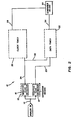
- Figs. 2, 3 and 4 show electrical circuits of the invention.
- FIG. 1a shows a sequence of bitcells. Each bitcell is defined by a variable time t i between two adjacent clock transitions. Within each bitcell, a data 0 bit or a data 1 bit has been encoded in accordance with the ratio as defined. For illustration purposes, a data 0 bit has been encoded by the ratio and a data 1 bit has been encoded by the ratio
- the method of decoding the encoded waveform of magnetic systems first requires the employment of a magnetic reader.
- the magnetic reader may provide a time derivative encoded waveform of that shown in FIG. 1A.
- This time derivative encoded waveform is shown in FIG. 1B.
- FIG. 1B shows an analog encoded waveform, comprising (albeit in a different form from FIG. 1A) the clock information mixed in with the data information.
- FIG. 1B shows that each bitcell is defined by the variable time t i , and that the clock information comprises negative pulses or valleys, and that the data information comprises positive pulses or peaks.
- the encoded waveform of FIG. 1B may be decoded by the step of determining the time between the first clock transition and the data transition, and comparing this time to the variable bitcell time t i .
- Preferred circuitry for realizing this step is shown in FIG. 2.
- FIG. 2 shows an electrical circuit 10 suitable for decoding the encoded signal waveform that carries clock information and data information i.e., the waveform of FIG. 1B.
- the structure of the electric circuit 10 is as follows.
- the electrical circuit 10 comprises a separator means 12 that receives the encoded signal waveform along a line 14.
- the separator means 12 comprises a negative peak detector 16, and a positive peak detector 18 connected in parallel with the negative peak detector 16.
- the positive peak detector 18 is connected in series along a line 20 to a data timer 22.
- the negative peak detector 16 is connected in parallel to the data timer 22 along a line 32, and in series along a line 24 to a clock timer 26.
- the clock timer 26, in turn, is connected in series along a line 28, to a comparer means 30.
- the data timer 22 is connected in series to the comparer means 30 along a line 34.
- the encoded waveform comprising clock information mixed in with the data information (FIG. 1B), is provided as an input along the line 14 to the separator means 12.
- the separator means 12 provides an output clock signal (CS) and an output data signal, for each of a succession of bitcells.
- the separator means 12 accomplishes this by way of the negative peak detector 16, that detects the encoded signal waveform for clock-information, and the positive peak detector 18, that detects the encoded signal waveform for data information.
- the negative peak detector 16 detects the encoded signal waveform for valleys, or negative pulses
- the positive peak detector 18 detects the encoded signal waveform for peaks, or positive pulses.
- the detector 16 outputs a clock signal (CS) pulse train (see FIG.
- the detector 18 outputs a data signal pulse train (see FIG. 1D) for input to the data timer 22 along the line 20.
- the clock timer 26 generates a clock parameter CP that is a measure of the time demarked between a first and a second clock signal pulse.
- CP may be equal to say, 106 units, or 90 units.
- the clock timer 26 generates the clock parameter CP, for input along the line 28 to the comparer means 30.
- the clock timer 26 is then reset to 0 units.
- a suitable clock timer 26 may be constructed using conventional digital counter circuits and oscillators.
- the clock timer 26 initiates its counting upon the advent of the first clock signal pulse.
- This first clock signal pulse is also imputted to the data timer 22 along the line 32.
- the data timer 22 begins to count, and it continues to count until it receives a sequential data signal pulse along the line 20.
- the final count corresponds to the data parameter.
- the data parameter is equal to 70 units for a first bitcell, and equal to 36 units for a second bitcell.
- the data timer 22 generates the data parameter for input along the line 34 to the comparer means 30.
- the data timer 22 is then reset to 0 units.
- a suitable data timer 22 may be constructed using conventional digital counter circuits, oscillators and logic circuits.
- the comparer means 30 inputs the clock parameter CP along the line 28, and the data parameter along the line 34.
- the comparer means 30 generates a new parameter, namely CP 2 .
- the importance of the parameter CP 2 is that it provides an indication of the halfway point of each bitcell.
- the comparer means 30 compares the data parameter for each bitcell, with that bitcell's parameter CP 2 .
- the comparer means 30 assigns a decoded signal a first valuation if the data parameter is less than CP 2 , and a second valuation if the data parameter is greater than CP 2 .
- Fig. 1e shows decoded data information for sequential bitcells; the information was previously embedded in the encoded waveform of Fig. 1a.
- FIG. 3 shows the electrical circuit 10 of Fig. 2, as well as a threshold circuit 36, a time out circuit 38, a counter timer 40, a multiplexer 42, a first logic circuit 44, and a second logic circuit 46.
- the threshold circuit 36 connected as shown between the separator means 12 and the clock timer 26 and the data timer 22, may be employed to suppress noise embedded in the Fig. 1b waveform, to minimize the effects of amplitude changes in the Fig. 1b waveform, and/or to provide a digital variant of the Fig. 1b waveform.
- the time out circuit 38 connected as shown as an output to the clock timer 26, preferably is employed to address the following problem.
- the electrical circuit 10 may input sequential bitcells of unacceptably long duration. Or, a sequential bitcell string may simply come to an end. In either case, the time out circuit 38 may be used to disable further input to the clock timer 26 after a preselected interval.
- the counter timer 40 and multiplexer 42 connected as shown between the clock timer 26, the comparer means 30 and the first logic circuit 44, address the following problem.
- the clock timer 26 inputs the Fig. 1c clock signal pulse train, and generates the clock parameter CP that is a measure of the time demarked between a first and second clock signal pulse.
- This capability implicitly suggests that a second clock signal pulse stops the clock timer 26 from counting, and, at the same time, initiates the start of the next bitcell. This situation suggests an instantaneous overlap of functions.
- the solution to this problem of overlapping functions may be provided by the counter timer 40/multiplexer 42 in combination with the logic circuit 44.
- the multiplexer 42 switches from a counter timer 48 to the independent, but otherwise functionally equivalent counter timer 40, per alternate bitcells.
- the multiplexer 42 switches from a counter timer 48 to the independent, but otherwise functionally equivalent counter timer 40, per alternate bitcells.
- the second logic circuit 46 comprising a suitable set-reset flip-flop, functions to implement one of the stated objectives of the clock timer 26 specified above. Namely, the second logic circuit 46 helps provide the instruction to the data timer 22, in particular, to a counter timer 50, to the end that it should begin counting.
- Fig. 4 shows another aspect of the present invention, namely, an electrical circuit 52 comprising a separator means 54 and a microprocessor 56.
- the separator means 54 inputs along a line 58 the encoded signal waveform of Fig. 1b, separates the clock information from the data information, and outputs along a line pair 60, 62, an output clock signal pulse train and an output data signal pulse train, for input to the microprocessor 56.
- the microprocessor 56 comprises a program that
Landscapes
- Engineering & Computer Science (AREA)
- Signal Processing (AREA)
- Theoretical Computer Science (AREA)
- Synchronisation In Digital Transmission Systems (AREA)
- Dc Digital Transmission (AREA)
Applications Claiming Priority (2)
| Application Number | Priority Date | Filing Date | Title |
|---|---|---|---|
| US206553 | 1988-06-14 | ||
| US07/206,553 US4876697A (en) | 1988-06-14 | 1988-06-14 | Three-part decoder circuit |
Publications (1)
| Publication Number | Publication Date |
|---|---|
| EP0346774A1 true EP0346774A1 (de) | 1989-12-20 |
Family
ID=22766893
Family Applications (1)
| Application Number | Title | Priority Date | Filing Date |
|---|---|---|---|
| EP89110493A Withdrawn EP0346774A1 (de) | 1988-06-14 | 1989-06-09 | Schaltung zur Dekodierung eines dreiteiligen Kodes |
Country Status (4)
| Country | Link |
|---|---|
| US (1) | US4876697A (de) |
| EP (1) | EP0346774A1 (de) |
| KR (1) | KR900702525A (de) |
| WO (1) | WO1989012891A1 (de) |
Cited By (1)
| Publication number | Priority date | Publication date | Assignee | Title |
|---|---|---|---|---|
| CN1042271C (zh) * | 1992-08-31 | 1999-02-24 | 三星电子株式会社 | 用于在数字记录和重放系统中计算直流值的电路 |
Families Citing this family (12)
| Publication number | Priority date | Publication date | Assignee | Title |
|---|---|---|---|---|
| US5251235A (en) * | 1988-06-14 | 1993-10-05 | Bengt Henoch | Single receiver for receiving wireless transmission of signals is for use with a serial two-conductor data bus |
| US5025328A (en) * | 1989-03-22 | 1991-06-18 | Eastman Kodak Company | Circuit for decoding binary information |
| US4979189A (en) * | 1989-08-18 | 1990-12-18 | National Semiconductor Corporation | Self-timing qualification channel |
| DK0489819T3 (da) * | 1989-08-31 | 1993-08-30 | Eastman Kodak Co | Forbedret dekodningskredsløb |
| US5420730A (en) * | 1990-08-17 | 1995-05-30 | Moon; Ronald R. | Servo data recovery circuit for disk drive having digital embedded sector servo |
| US5438461A (en) * | 1991-07-19 | 1995-08-01 | Canon Kabushiki Kaisha | Magnetic reproduction apparatus for a camera |
| US5204708A (en) * | 1991-12-20 | 1993-04-20 | Eastman Kodak Company | Method and apparatus for magnetically communicating via a photographic filmstrip with enhanced reliability |
| US5396240A (en) * | 1993-09-01 | 1995-03-07 | Maxtor Corporation | Missing pulse generator for gray code decoding |
| US5825319A (en) * | 1996-12-23 | 1998-10-20 | Analog Devices, Inc. | High speed wide bandwidth digital peak detector |
| US6493514B1 (en) | 2001-09-04 | 2002-12-10 | Eastman Kodak Company | Method and apparatus for magnetic communication via a photographic filmstrip |
| US7535964B2 (en) * | 2005-08-31 | 2009-05-19 | Maxim Integrated Products, Inc. | Self-clocked two-level differential signaling methods and apparatus |
| KR101866486B1 (ko) * | 2011-01-25 | 2018-06-12 | 에스케이하이닉스 주식회사 | 온도 감지 회로 |
Citations (1)
| Publication number | Priority date | Publication date | Assignee | Title |
|---|---|---|---|---|
| GB1542398A (en) * | 1976-05-24 | 1979-03-21 | Secr Defence | Recording data |
Family Cites Families (4)
| Publication number | Priority date | Publication date | Assignee | Title |
|---|---|---|---|---|
| GB1170684A (en) * | 1967-01-20 | 1969-11-12 | English Electric Co Ltd | Improvements in Electrical Relays |
| US4357634A (en) * | 1979-10-01 | 1982-11-02 | Chung David H | Encoding and decoding digital information utilizing time intervals between pulses |
| US4592072B1 (en) * | 1982-05-07 | 1994-02-15 | Digital Equipment Corporation | Decoder for self-clocking serial data communications |
| US4689802A (en) * | 1986-05-22 | 1987-08-25 | Chrysler Motors Corporation | Digital pulse width modulator |
-
1988
- 1988-06-14 US US07/206,553 patent/US4876697A/en not_active Expired - Fee Related
-
1989
- 1989-06-05 KR KR1019900700300A patent/KR900702525A/ko not_active Withdrawn
- 1989-06-05 WO PCT/US1989/002430 patent/WO1989012891A1/en not_active Ceased
- 1989-06-09 EP EP89110493A patent/EP0346774A1/de not_active Withdrawn
Patent Citations (1)
| Publication number | Priority date | Publication date | Assignee | Title |
|---|---|---|---|---|
| GB1542398A (en) * | 1976-05-24 | 1979-03-21 | Secr Defence | Recording data |
Cited By (1)
| Publication number | Priority date | Publication date | Assignee | Title |
|---|---|---|---|---|
| CN1042271C (zh) * | 1992-08-31 | 1999-02-24 | 三星电子株式会社 | 用于在数字记录和重放系统中计算直流值的电路 |
Also Published As
| Publication number | Publication date |
|---|---|
| US4876697A (en) | 1989-10-24 |
| WO1989012891A1 (en) | 1989-12-28 |
| KR900702525A (ko) | 1990-12-07 |
Similar Documents
| Publication | Publication Date | Title |
|---|---|---|
| EP0346774A1 (de) | Schaltung zur Dekodierung eines dreiteiligen Kodes | |
| US4146743A (en) | Adaptive sampling decoder-encoder apparatus and method | |
| US4045767A (en) | Method of ultrasonic data communication and apparatus for carrying out the method | |
| US4317211A (en) | Manchester code decoding apparatus | |
| JP2621884B2 (ja) | 通信方法及び符号化装置 | |
| US4307381A (en) | Method and means for encoding and decoding digital data | |
| US3968328A (en) | Circuit for automatically correcting the timing of clock pulse in self-clocked pulse signal decoders | |
| US4204199A (en) | Method and means for encoding and decoding digital data | |
| US4292626A (en) | Manchester decoder | |
| IE791412L (en) | Signal decoding | |
| US4567604A (en) | Biphase signal receiver | |
| US4860324A (en) | Information data recovering apparatus | |
| WO1990011650A1 (en) | Digital circuit for encoding binary information | |
| EP0346777A1 (de) | Schaltung zur Kodierung eines dreiteiligen Kodes | |
| JPH04501047A (ja) | 自己クロッキング符号化データのためのデータ配列回路及び方法 | |
| EP0346776A1 (de) | Schaltung zur Dekodierung eines dreiteiligen Kodes | |
| US5454006A (en) | Method and apparatus for bandwidth limited binary signals | |
| US3493962A (en) | Converter for self-clocking digital signals | |
| US6115548A (en) | Method and apparatus for interfacing data signal and associated clock signal to circuit controlled by local clock signal | |
| SU1520591A1 (ru) | Способ управлени одноразр дным запоминающим устройством на ферритовых сердечниках и устройство дл его осуществлени | |
| JP2696812B2 (ja) | クロックパルス再生装置 | |
| GB1442444A (en) | Signal decoder | |
| SU957260A2 (ru) | Устройство цифровой магнитной записи | |
| SU652558A1 (ru) | Устройство дл сортировки чисел | |
| SU1531154A1 (ru) | Устройство дл преобразовани двоичной последовательности в фазомодулированный сигнал |
Legal Events
| Date | Code | Title | Description |
|---|---|---|---|
| PUAI | Public reference made under article 153(3) epc to a published international application that has entered the european phase |
Free format text: ORIGINAL CODE: 0009012 |
|
| AK | Designated contracting states |
Kind code of ref document: A1 Designated state(s): ES |
|
| STAA | Information on the status of an ep patent application or granted ep patent |
Free format text: STATUS: THE APPLICATION IS DEEMED TO BE WITHDRAWN |
|
| 18D | Application deemed to be withdrawn |
Effective date: 19900621 |