EP0345049B1 - Vorrichtung zur Aufnahme thermischer Bilder - Google Patents
Vorrichtung zur Aufnahme thermischer Bilder Download PDFInfo
- Publication number
- EP0345049B1 EP0345049B1 EP89305496A EP89305496A EP0345049B1 EP 0345049 B1 EP0345049 B1 EP 0345049B1 EP 89305496 A EP89305496 A EP 89305496A EP 89305496 A EP89305496 A EP 89305496A EP 0345049 B1 EP0345049 B1 EP 0345049B1
- Authority
- EP
- European Patent Office
- Prior art keywords
- layer
- pyroelectric
- electrodes
- electrode
- patches
- Prior art date
- Legal status (The legal status is an assumption and is not a legal conclusion. Google has not performed a legal analysis and makes no representation as to the accuracy of the status listed.)
- Expired - Lifetime
Links
Images


Classifications
-
- G—PHYSICS
- G01—MEASURING; TESTING
- G01J—MEASUREMENT OF INTENSITY, VELOCITY, SPECTRAL CONTENT, POLARISATION, PHASE OR PULSE CHARACTERISTICS OF INFRARED, VISIBLE OR ULTRAVIOLET LIGHT; COLORIMETRY; RADIATION PYROMETRY
- G01J5/00—Radiation pyrometry, e.g. infrared or optical thermometry
- G01J5/10—Radiation pyrometry, e.g. infrared or optical thermometry using electric radiation detectors
- G01J5/34—Radiation pyrometry, e.g. infrared or optical thermometry using electric radiation detectors using capacitors, e.g. pyroelectric capacitors
-
- H—ELECTRICITY
- H10—SEMICONDUCTOR DEVICES; ELECTRIC SOLID-STATE DEVICES NOT OTHERWISE PROVIDED FOR
- H10N—ELECTRIC SOLID-STATE DEVICES NOT OTHERWISE PROVIDED FOR
- H10N15/00—Thermoelectric devices without a junction of dissimilar materials; Thermomagnetic devices, e.g. using the Nernst-Ettingshausen effect
- H10N15/10—Thermoelectric devices using thermal change of the dielectric constant, e.g. working above and below the Curie point
Definitions
- This invention relates to a thermal imaging device comprising an array of pyroelectric detector elements formed by electrodes carried on the opposing major surfaces of a thin film layer of pyroelectric material, the pyroelectric layer extending over a substrate layer carrying a plurality of electrical signal processing circuits and being supported from the substrate layer by a plurality of pillars which additionally provide electrical connection between the detector elements and the electrical circuits.
- each thermal detector electrode is directly supported by a pillar containing conductive paths. This results in thermal conduction which impairs performance.
- An object of the present invention is to provide an alternative thermal imaging device in which the pyroelectric detector elements are supported by pillars but wherein thermal conduction between the pillars and detector elements is reduced.
- thermo imaging device as defined in the first paragraph above is characterised by the combination of:
- the pyroelectric material may comprise material which is inherently pyroelectric, or material whose pyroelectric characteristics are induced (e.g. by appropriate poling of ferroelectric material).
- the layer is suitably a thin film of pyroelectric material.
- the elongate strip suitably has a length to width ratio of at least 5.
- Patent Abstracts of Japan vol.10 no. 232 p.486 discloses a planar self supporting array having elongate strips of electrically conducting material extending from the discrete electrodes to provide electrical connections close to the edge of the device, and achieves thermal separation between elements by drilling holes in the pyroelectric array.
- the discrete electrodes are arranged in rows and columns and said electrically conductive regions are situated at the centres of respective rectangles formed by the centres of four adjacent discrete electrodes.
- the discrete electrodes are arranged in interleaved rows and interleaved columns and the electrically conductive regions are situated at the centres of respective triangles formed by the centres of three adjacent, discrete electrodes.
- respective supplementary electrodes are provided in the non-electroded regions of the other major surface between each discrete electrode and the adjacent pillars, each supplementary electrode being connected to a respective pillar, the pillar having two independent electrically conductive paths to the signal processing means.
- an improved signal/noise ratio may be achieved.
- received infrared radiation incident on the nonelectroded regions of the layer is diverted into the electroded regions by an optical arrangement.
- a pyroelectric film 21, of for example, polyvinylidene fluoride (PVDF) has a pattern of interconnected electrodes 22 formed on one side and a pattern of discrete electrodes 23 and electrically conductive patches 24 formed on the other side.
- the discrete electrodes 23 are linked to respective patches 24 by narrow electrically conductive strips 25.
- Electrically conductive pillars 26 are bonded at one end to respective patches 24 and at the other end to input pads 27 of an integrated circuit 28 formed on the substrate 29.
- the discrete electrodes 23 are arranged in rows and columns and the patches 24 are arranged in rows and columns which interleave those of the discrete electrodes 23.
- the electrodes 22 and 23 are each of equal size and the patches 24 and pillars 26 are also of equal size, but smaller than the electrodes. Also in this example the electrodes, patches and pillars are all square and arranged so that each of the inter-connected patches and electrodes has one face perpendicular to the conductive strip joining the patch and electrode.
- the inter-connected electrodes 22 are covered by an infrared absorbent layer 30, for example a layer of black gold.
- the inter-connections between these electrodes 22 should be narrow, thin and preferably meandered to increase their length.
- the interconnected electrodes are connected to ground.
- the discrete electrodes 23 are arranged in interleaved rows and columns and the patches 24 are arranged at the centres of the triangles formed by three adjacent electrodes 23, each patch being connected to a respective electrode by a narrow conductor 25.
- the construction of this embodiment is similar to that described hereinbefore with reference to Figure 1.
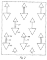
- each discrete electrode 23 has an area around it in which the received radiation is wasted. This is overcome in the third device to be described by the provision of a supplementary electrode around the electrode 23, as shown at 51 in Figure 3.
- the arrangement of electrodes 23 is the same as in Figure 1, but the conducting patches 24 are each split into two patches 24a, 24b.
- Each electrode 23 is connected to a corresponding patch 24a by the narrow conductor 25 and each of the extra electrodes 51 is connected to the corresponding patch 24b by the narrow conductor 52.
- the two patches 24a, 24b are connected to a respective one of a respective pair of input pads of an integrated circuit either by a pair of electrically conductive pillars (not shown) or by an insulative pillar (also not shown) carrying two electrically conductive tracks.
- Both inputs to the processing means are pre-amplified, weighted and added.
- the supplementary electrode has higher thermal losses than the discrete electrode, so the supplementary electrode output is given a lower weighting than the discrete electrode output, but is still able to improve the signal/noise ratio.
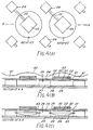
- a plate 61 transparent to infrared covers the array of inter-connected electrodes 30 and is profiled to provide convex surfaces 62 over each electrode area so that received radiation is concentrated towards the electrode area.
- the plate 61 is replaced by concave reflecting surfaces 63 positioned behind each discrete electrode 23, the plate reflecting the energy received around the electrodes back towards the electrodes.
- an infrared absorbent layer for example a layer of black gold, to absorb the energy reflected back by the concave surface 63.
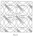
- the sixth device to be described includes two further means for reducing the thermal losses from the pyroelectric detector elements. Firstly the thermal conductance from the electrodes 23 to the corresponding patch 24 and pillar 26 is reduced by replacing the straight narrow conductors in the arrangements of Figures 1 and 2 by meandering conductors 71. Secondly, thermal conductance through the pyroelectric film 21 is reduced by forming holes 72 in the pyroelectric film. Either of these arrangements could also be used with the electrode arrangements of Figure 2. In Figure 5, the electrodes 23 and patches 24 are smaller than in Figure 1, facilitating the use of narrow strips of film 73 between the pairs of adjacent holes 72.
- a convex lens 62 transparent to infrared may be placed over each inter-connected electrode 22, as at 62 in Figure 4b, or a concave mirror 63 may be placed under each discrete electrode 23, as at 63 in Figure 4c.
- the lenses 62 or mirrors 63 are shown schematically as circles in Figure 5.
- the electrodes can be of a complex shape; in an advantageous form, the shape of the electrodes conforms to the isothermal-resistance contours of the device, such that the electrodes are located in regions wherein the thermal resistance to ground has a relatively high value (preferably being at its highest).
- the outer boundary of the inner electrode and the inner boundary of the outer electrode have a similar shape in accordance with the isothermal-resistance contours of the locality, and not necessarily similar to the shape of the outer boundary of the outer electrode which is in accordance with the isothermal-resistance contours of the respective locality.
Landscapes
- Engineering & Computer Science (AREA)
- Power Engineering (AREA)
- Physics & Mathematics (AREA)
- General Physics & Mathematics (AREA)
- Spectroscopy & Molecular Physics (AREA)
- Transforming Light Signals Into Electric Signals (AREA)
- Photometry And Measurement Of Optical Pulse Characteristics (AREA)
- Radiation Pyrometers (AREA)
- Color Television Image Signal Generators (AREA)
- Solid State Image Pick-Up Elements (AREA)
- Carbon And Carbon Compounds (AREA)
- Light Receiving Elements (AREA)
Claims (5)
- Thermische Abbildungsvorrichtung mit einer Anordnung pyroelektrischer Detektorelemente, die durch Elektroden (22, 23) ausgebildet sind, welche auf den entgegengesetzten Hauptoberflächen einer dünnen Filmschicht (21) aus pyroelektrischem Material getragen sind, wobei sich die pyroelektrische Schicht (21) über einer Substratschicht (29) erstreckt, welche eine Mehrzahl von Signalverarbeitungsstromkreisen (28) trägt, und von der Substratschicht (29) durch eine Mehrzahl von Säulen (26) gestützt ist, welche zusätzlich eine elektrische Verbindung zwischen den Detektorelementen und den Stromkreisen (28) schaffen,
gekennzeichnet durch folgende Kombination:a) beide Hauptoberflächen der pyroelektrischen Schicht (21) tragen eine Mehrzahl einzelner Elektroden (22, 23), welche kooperieren, um die Detektorelemente zu bilden, wobei die entsprechenden Elektroden auf jeder Oberfläche der pyroelektrischen Schicht voneinander beabstandet sind, um Bereiche ohne Elektroden der Oberflächen freizulassen;b) die einzelnen Elektroden (22) auf der von der Substratschicht (29) entfernten Oberfläche der pyroelektrischen Schicht sind elektrisch miteinander verbunden;c) die Hauptoberfläche der pyroelektrischen Schicht (21), die zu der Substratschicht (29) benachbart ist, trägt zusätzlich eine Mehrzahl elektrisch leitender Elemente (24), welche in einem Bereich ohne Elektroden der pyroelektrischen Schicht (21) ausgebildet sind und seitlich von den Detektorelementen (21, 22, 23) beabstandet sind, wobei jedes Element (24) jeweils elektrisch mit einer Elektrode (23) auf derselben Hauptoberfläche durch einen Längsstreifen (25) aus elektrisch leitendem Material verbunden ist;d) jeder Längsstreifen (25) weist ein Verhältnis Länge zu Breite von mindestens 5 auf; unde) die Säulen (26) erstrecken sich von den Elementen (24) zu der Substratschicht (29). - Vorrichtung gemäß Anspruch 1, gekennzeichnet durch entsprechende zusätzliche Elektroden (51), welche um jede Elektrode (23) auf der der Substratschicht (29) benachbarten Hauptoberfläche der pyroelektrischen Schicht (21) und in einem Oberflächenbereich ohne Elektroden zur Verfügung gestellt sind, wobei jede zusätzliche Elektrode (51) mit derselben Säule (26) verbunden ist, wie die Elektrode (23), um welche sie angeordnet ist, wobei jede Säule (26) zwei unabhängige elektrisch leitende Pfade zu dem betreffenden Signalverarbeitungsstromkreis (28) aufweist.
- Vorrichtung gemäß einem der vorhergehenden Ansprüche mit einer optischen Anordnung (61, 63), welche zur Ablenkung von Infrarotstrahlung, welche auf die Bereiche ohne Elektroden der pyroelektrischen Schicht (21) auftrifft, in die Elektrodenbereiche wirksam ist.
- Vorrichtung gemäß Anspruch 3, bei der es sich bei der optischen Anordnung um eine Linsenanordnung (61, 62) zwischen der Strahlungsquelle und der pyroelektrischen Schicht (21) handelt.
- Vorrichtung gemäß Anspruch 3, bei der es sich bei der optischen Anordnung um eine Reflexionsanordnung (63) zwischen der pyroelektrischen Schicht (21) und den Signalverarbeitungsstromkreisen (28) handelt.
Applications Claiming Priority (2)
| Application Number | Priority Date | Filing Date | Title |
|---|---|---|---|
| GB8812957 | 1988-06-01 | ||
| GB888812957A GB8812957D0 (en) | 1988-06-01 | 1988-06-01 | Thermal imaging |
Publications (3)
| Publication Number | Publication Date |
|---|---|
| EP0345049A2 EP0345049A2 (de) | 1989-12-06 |
| EP0345049A3 EP0345049A3 (en) | 1990-10-03 |
| EP0345049B1 true EP0345049B1 (de) | 1996-05-01 |
Family
ID=10637883
Family Applications (1)
| Application Number | Title | Priority Date | Filing Date |
|---|---|---|---|
| EP89305496A Expired - Lifetime EP0345049B1 (de) | 1988-06-01 | 1989-05-31 | Vorrichtung zur Aufnahme thermischer Bilder |
Country Status (7)
| Country | Link |
|---|---|
| US (1) | US4996428A (de) |
| EP (1) | EP0345049B1 (de) |
| JP (1) | JP2806972B2 (de) |
| AT (1) | ATE137610T1 (de) |
| CA (1) | CA1323903C (de) |
| DE (1) | DE68926363T2 (de) |
| GB (1) | GB8812957D0 (de) |
Families Citing this family (4)
| Publication number | Priority date | Publication date | Assignee | Title |
|---|---|---|---|---|
| GB9009117D0 (en) * | 1990-04-24 | 1990-08-08 | Emi Plc Thorn | Pyroelectric detector and method of manufacturing the same |
| GB2274543A (en) * | 1993-01-21 | 1994-07-27 | Central Research Lab Ltd | Infrared detector |
| JPH07286894A (ja) * | 1994-04-18 | 1995-10-31 | Fujitsu Ltd | 赤外線検知装置の製造方法 |
| US10651095B2 (en) * | 2016-08-11 | 2020-05-12 | Applied Materials, Inc. | Thermal profile monitoring wafer and methods of monitoring temperature |
Family Cites Families (6)
| Publication number | Priority date | Publication date | Assignee | Title |
|---|---|---|---|---|
| GB2035685B (en) * | 1978-10-28 | 1983-05-05 | Plessey Co Ltd | Pyroelectric detectors |
| US4737642A (en) * | 1983-04-21 | 1988-04-12 | Licentia Patent-Verwaltungs-Gmbh | Arrangement for multispectral imaging of objects, preferably targets |
| US4593456A (en) * | 1983-04-25 | 1986-06-10 | Rockwell International Corporation | Pyroelectric thermal detector array |
| GB2163596B (en) * | 1984-08-24 | 1988-02-03 | Philips Electronic Associated | A thermal imaging device and a method of manufacturing a thermal imaging device |
| US4701618A (en) * | 1985-05-28 | 1987-10-20 | Galileo Electro-Optics Corp. | Middle-infrared imaging device |
| US4754139A (en) * | 1986-04-10 | 1988-06-28 | Aerojet-General Corporation | Uncooled high resolution infrared imaging plane |
-
1988
- 1988-06-01 GB GB888812957A patent/GB8812957D0/en active Pending
-
1989
- 1989-05-31 EP EP89305496A patent/EP0345049B1/de not_active Expired - Lifetime
- 1989-05-31 DE DE68926363T patent/DE68926363T2/de not_active Expired - Fee Related
- 1989-05-31 CA CA000601292A patent/CA1323903C/en not_active Expired - Fee Related
- 1989-05-31 AT AT89305496T patent/ATE137610T1/de not_active IP Right Cessation
- 1989-06-01 US US07/359,881 patent/US4996428A/en not_active Expired - Fee Related
- 1989-06-01 JP JP1137599A patent/JP2806972B2/ja not_active Expired - Lifetime
Non-Patent Citations (2)
| Title |
|---|
| & JP-A- 62 119422 (MATSUSHITA) 30 May 1987, * |
| Patent Abstracts of Japan, vol.10, no.15 (P-422)[2072] 21 January 1986 * |
Also Published As
| Publication number | Publication date |
|---|---|
| CA1323903C (en) | 1993-11-02 |
| JPH02236129A (ja) | 1990-09-19 |
| JP2806972B2 (ja) | 1998-09-30 |
| EP0345049A2 (de) | 1989-12-06 |
| US4996428A (en) | 1991-02-26 |
| EP0345049A3 (en) | 1990-10-03 |
| ATE137610T1 (de) | 1996-05-15 |
| GB8812957D0 (en) | 1988-10-05 |
| DE68926363D1 (de) | 1996-06-05 |
| DE68926363T2 (de) | 1996-11-28 |
Similar Documents
| Publication | Publication Date | Title |
|---|---|---|
| US6049080A (en) | Pyroelectric infrared sensor device | |
| US4558365A (en) | High-resolution high-sensitivity solid-state imaging sensor | |
| US4593456A (en) | Pyroelectric thermal detector array | |
| US4532424A (en) | Pyroelectric thermal detector array | |
| US4029962A (en) | Arrays for infrared image detection | |
| US4403238A (en) | Detector array focal plane configuration | |
| US4575631A (en) | Infra-red detector | |
| US4209347A (en) | Mounting for solar cell | |
| SE8702531L (sv) | Termisk detektoruppsaettning | |
| IL122429A (en) | Electromagnetic wave detector | |
| JPH07218337A (ja) | 放射検出装置及び該装置の製造方法 | |
| EP0345047B1 (de) | Vorrichtung zur Aufnahme thermischer Bilder | |
| EP0345049B1 (de) | Vorrichtung zur Aufnahme thermischer Bilder | |
| US7232998B2 (en) | Bolometer-type infrared solid-state image sensor | |
| US4695861A (en) | Backside mosaic photoconductive infrared detector array | |
| EP0375205B1 (de) | Vorrichtung zur thermischen Abbildung | |
| US6512809B2 (en) | Radiation detector for an X-ray computed tomography apparatus | |
| JPH0821767A (ja) | 赤外線検出器及びその製造方法 | |
| US4859851A (en) | Thermal-radiation imaging devices and systems, and the manufacture of such imaging devices | |
| JPS637611B2 (de) | ||
| US4475040A (en) | Pyroelectric infrared detector | |
| US4942301A (en) | Thermal imaging device | |
| US4900367A (en) | Method of making a reticulated temperature sensitive imaging device | |
| JPH0734482B2 (ja) | 光結合型半導体リレ−装置 | |
| US5315100A (en) | Photoelectric conversion apparatus for detecting movement of object with spatial filter electrode |
Legal Events
| Date | Code | Title | Description |
|---|---|---|---|
| PUAI | Public reference made under article 153(3) epc to a published international application that has entered the european phase |
Free format text: ORIGINAL CODE: 0009012 |
|
| AK | Designated contracting states |
Kind code of ref document: A2 Designated state(s): AT BE CH DE ES FR GB GR IT LI LU NL SE |
|
| PUAL | Search report despatched |
Free format text: ORIGINAL CODE: 0009013 |
|
| AK | Designated contracting states |
Kind code of ref document: A3 Designated state(s): AT BE CH DE ES FR GB GR IT LI LU NL SE |
|
| 17P | Request for examination filed |
Effective date: 19910327 |
|
| 17Q | First examination report despatched |
Effective date: 19930512 |
|
| RAP1 | Party data changed (applicant data changed or rights of an application transferred) |
Owner name: PILKINGTON THORN OPTRONICS LIMITED |
|
| GRAA | (expected) grant |
Free format text: ORIGINAL CODE: 0009210 |
|
| AK | Designated contracting states |
Kind code of ref document: B1 Designated state(s): AT BE CH DE ES FR GB GR IT LI LU NL SE |
|
| PG25 | Lapsed in a contracting state [announced via postgrant information from national office to epo] |
Ref country code: IT Free format text: LAPSE BECAUSE OF FAILURE TO SUBMIT A TRANSLATION OF THE DESCRIPTION OR TO PAY THE FEE WITHIN THE PRESCRIBED TIME-LIMIT;WARNING: LAPSES OF ITALIAN PATENTS WITH EFFECTIVE DATE BEFORE 2007 MAY HAVE OCCURRED AT ANY TIME BEFORE 2007. THE CORRECT EFFECTIVE DATE MAY BE DIFFERENT FROM THE ONE RECORDED. Effective date: 19960501 Ref country code: BE Effective date: 19960501 Ref country code: GR Free format text: LAPSE BECAUSE OF FAILURE TO SUBMIT A TRANSLATION OF THE DESCRIPTION OR TO PAY THE FEE WITHIN THE PRESCRIBED TIME-LIMIT Effective date: 19960501 Ref country code: LI Free format text: LAPSE BECAUSE OF FAILURE TO SUBMIT A TRANSLATION OF THE DESCRIPTION OR TO PAY THE FEE WITHIN THE PRESCRIBED TIME-LIMIT Effective date: 19960501 Ref country code: AT Effective date: 19960501 Ref country code: ES Free format text: THE PATENT HAS BEEN ANNULLED BY A DECISION OF A NATIONAL AUTHORITY Effective date: 19960501 Ref country code: NL Free format text: LAPSE BECAUSE OF FAILURE TO SUBMIT A TRANSLATION OF THE DESCRIPTION OR TO PAY THE FEE WITHIN THE PRESCRIBED TIME-LIMIT Effective date: 19960501 Ref country code: CH Free format text: LAPSE BECAUSE OF FAILURE TO SUBMIT A TRANSLATION OF THE DESCRIPTION OR TO PAY THE FEE WITHIN THE PRESCRIBED TIME-LIMIT Effective date: 19960501 |
|
| REF | Corresponds to: |
Ref document number: 137610 Country of ref document: AT Date of ref document: 19960515 Kind code of ref document: T |
|
| PG25 | Lapsed in a contracting state [announced via postgrant information from national office to epo] |
Ref country code: LU Free format text: LAPSE BECAUSE OF NON-PAYMENT OF DUE FEES Effective date: 19960531 |
|
| REF | Corresponds to: |
Ref document number: 68926363 Country of ref document: DE Date of ref document: 19960605 |
|
| PG25 | Lapsed in a contracting state [announced via postgrant information from national office to epo] |
Ref country code: SE Effective date: 19960801 |
|
| ET | Fr: translation filed | ||
| NLV1 | Nl: lapsed or annulled due to failure to fulfill the requirements of art. 29p and 29m of the patents act | ||
| REG | Reference to a national code |
Ref country code: CH Ref legal event code: PL |
|
| PLBE | No opposition filed within time limit |
Free format text: ORIGINAL CODE: 0009261 |
|
| STAA | Information on the status of an ep patent application or granted ep patent |
Free format text: STATUS: NO OPPOSITION FILED WITHIN TIME LIMIT |
|
| 26N | No opposition filed | ||
| PGFP | Annual fee paid to national office [announced via postgrant information from national office to epo] |
Ref country code: DE Payment date: 19970606 Year of fee payment: 9 |
|
| PGFP | Annual fee paid to national office [announced via postgrant information from national office to epo] |
Ref country code: FR Payment date: 19980511 Year of fee payment: 10 |
|
| PGFP | Annual fee paid to national office [announced via postgrant information from national office to epo] |
Ref country code: GB Payment date: 19980522 Year of fee payment: 10 |
|
| PG25 | Lapsed in a contracting state [announced via postgrant information from national office to epo] |
Ref country code: DE Free format text: LAPSE BECAUSE OF NON-PAYMENT OF DUE FEES Effective date: 19990302 |
|
| PG25 | Lapsed in a contracting state [announced via postgrant information from national office to epo] |
Ref country code: GB Free format text: LAPSE BECAUSE OF NON-PAYMENT OF DUE FEES Effective date: 19990531 |
|
| GBPC | Gb: european patent ceased through non-payment of renewal fee |
Effective date: 19990531 |
|
| PG25 | Lapsed in a contracting state [announced via postgrant information from national office to epo] |
Ref country code: FR Free format text: LAPSE BECAUSE OF NON-PAYMENT OF DUE FEES Effective date: 20000131 |
|
| REG | Reference to a national code |
Ref country code: FR Ref legal event code: ST |