EP0345049A2 - Vorrichtung zur Aufnahme thermischer Bilder - Google Patents
Vorrichtung zur Aufnahme thermischer BilderInfo
- Publication number
- EP0345049A2 EP0345049A2 EP89305496A EP89305496A EP0345049A2 EP 0345049 A2 EP0345049 A2 EP 0345049A2 EP 89305496 A EP89305496 A EP 89305496A EP 89305496 A EP89305496 A EP 89305496A EP 0345049 A2 EP0345049 A2 EP 0345049A2
- Authority
- EP
- European Patent Office
- Prior art keywords
- electrodes
- electrically conductive
- discrete
- layer
- electrode
- Prior art date
- Legal status (The legal status is an assumption and is not a legal conclusion. Google has not performed a legal analysis and makes no representation as to the accuracy of the status listed.)
- Granted
Links
Images

Classifications
-
- G—PHYSICS
- G01—MEASURING; TESTING
- G01J—MEASUREMENT OF INTENSITY, VELOCITY, SPECTRAL CONTENT, POLARISATION, PHASE OR PULSE CHARACTERISTICS OF INFRARED, VISIBLE OR ULTRAVIOLET LIGHT; COLORIMETRY; RADIATION PYROMETRY
- G01J5/00—Radiation pyrometry, e.g. infrared or optical thermometry
- G01J5/10—Radiation pyrometry, e.g. infrared or optical thermometry using electric radiation detectors
- G01J5/34—Radiation pyrometry, e.g. infrared or optical thermometry using electric radiation detectors using capacitors, e.g. pyroelectric capacitors
-
- H—ELECTRICITY
- H10—SEMICONDUCTOR DEVICES; ELECTRIC SOLID-STATE DEVICES NOT OTHERWISE PROVIDED FOR
- H10N—ELECTRIC SOLID-STATE DEVICES NOT OTHERWISE PROVIDED FOR
- H10N15/00—Thermoelectric devices without a junction of dissimilar materials; Thermomagnetic devices, e.g. using the Nernst-Ettingshausen effect
- H10N15/10—Thermoelectric devices using thermal change of the dielectric constant, e.g. working above and below the Curie point
Definitions
- This invention relates to thermal imaging devices and in particular to thermal imaging devices comprising an array of pyroelectric detector elements responsive to infrared radiation.
- the main factor limiting the performance of existing pyroelectric imaging devices in detecting an image of a scene focussed on the array of pyroelectric detector elements is the thermal conductance between adjacent detector elements and between each detector element and the supporting and interrogating structure.
- U.K. Patent Application No. 2163596A discloses a thermal imaging device comprising a ferroelectric slab bearing a common electrode on one main surface and a signal electrode structure on the opposite main surface.
- the signal electrode structure is electrically connected to electrodes of a circuit substrate by means of conductors
- the transverse heat conduction between adjacent conductors is reduced by incorporating conductors each in a respective pillar of thermally insulating material, the pillars also being effective to support the ferroelectric slab.
- It is an object of the present invention is to provide an alternative thermal imaging device in which the pyroelectric detector elements are supported by pillars but wherein the thermal losses between the detector elements and supporting pillars are reduced.
- a thermal imaging device comprises: a layer comprising pyroelectric material; an array of interconnected electrodes carried on one major surface of the layer; an array of discrete electrodes carried on the other major surface of the layer; a plurality of pillars effective to support the layer and to cause the passage of electrical signals between the discrete electrodes and an electrical signal processing means, each pillar being located at a respective electrically conductive region formed on said other major surface, each discrete electrode being separated from, but not substantially surrounding, a respective one of the first electrically conductive regions, each discrete electrode and respective electrically conductive region being electrically connected by a respective elongate strip of electrically conductive material.
- the pyroelectric material may comprise material which is inherently pyroelectric, or material whose pyroelectric characteristics are induced (e.g. by appropriate poling of ferroelectric material).
- the layer is suitably a thin film of pyroelectric material.
- the elongate strip suitably has a length to width ratio of at least 5.
- the discrete electrodes are arranged in rows and columns and said electrically conductive regions are situated at the centres of respective rectangles formed by the centres of four adjacent discrete electrodes.
- the discrete electrodes are arranged in interleaved rows and interleaved columns and the electrically conductive regions are situated at the centres of respective triangles formed by the centres of three adjacent, discrete electrodes.
- respective supplementary electrodes are provided in the non-electroded regions of the other major surface between each discrete electrode and the adjacent pillars, each supplementary electrode being connected to a respective pillar, the pillar having two independent electrically conductive paths to the signal processing means.
- an improved signal/noise ratio may be achieved.
- received infrared radiation incident on the nonelectroded regions of the layer is diverted into the electroded regions by an optical arrangement.
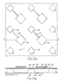
- a pyroelectric film 21, of for example, polyvinylidene fluoride (PVDF) has a pattern of interconnected electrodes 22 formed on one side and a pattern of discrete electrodes 23 and electrically conductive patches 24 formed on the other side.
- the discrete electrodes 23 are linked to respective patches 24 by narrow electrically conductive strips 25.
- Electrically conductive pillars 26 are bonded at one end to respective patches 24 and at the other end to input pads 27 of an integrated circuit 28 formed on the substrate 29.
- the discrete electrodes 23 are arranged in rows and columns and the patches 24 are arranged in rows and columns which interleave those of the discrete electrodes 23.
- the electrodes 22 and 23 are each of equal size and the patches 24 and pillars 26 are also of equal size, but smaller than the electrodes. Also in this example the electrodes, patches and pillars are all square and arranged so that each of the inter-connected patches and electrodes has one face perpendicular to the conductive strip joining the patch and electrode.
- the inter-connected electrodes 22 are covered by an infrared absorbent layer 30, for example a layer of black gold.
- the inter-connections between these electrodes 22 should be narrow, thin and preferably meandered to increase their length.
- the interconnected electrodes are connected to ground.
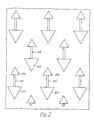
- the discrete electrodes 23 are arranged in interleaved rows and columns and the patches 24 are arranged at the centres of the triangles formed by three adjacent electrodes 23, each patch being connected to a respective electrode by a narrow conductor 25.
- the construction of this embodiment is similar to that described hereinbefore with reference to Figure 1.
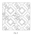
- each discrete electrode 23 has an area around it in which the received radiation is wasted. This is overcome in the third device to be described by the provision of a supplementary electrode around the electrode 23, as shown at 51 in Figure 3.
- the arrangement of electrodes 23 is the same as in Figure 1, but the conducting patches 24 are each split into two patches 24a, 24b.
- Each electrode 23 is connected to a corresponding patch 24a by the narrow conductor 25 and each of the extra electrodes 51 is connected to the corresponding patch 24b by the narrow conductor 52.
- the two patches 24a, 24b are connected to a respective one of a respective pair of input pads of an integrated circuit either by a pair of electrically conductive pillars (not shown) or by an insulative pillar (also not shown) carrying two electrically conductive tracks.
- Both inputs to the processing means are pre-amplified, weighted and added.
- the supplementary electrode has higher thermal losses than the discrete electrode, so the supplementary electrode output is given a lower weighting than the discrete electrode output, but is still able to improve the signal/noise ratio.
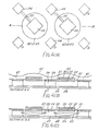
- a plate 61 transparent to infrared covers the array of inter-connected electrodes 30 and is profiled to provide convex surfaces 62 over each electrode area so that received radiation is concentrated towards the electrode area.
- the plate 61 is replaced by concave reflecting surfaces 63 positioned behind each discrete electrode 23, the plate reflecting the energy received around the electrodes back towards the electrodes.
- an infrared absorbent layer for example a layer of black gold, to absorb the energy reflected back by the concave surface 63.
- the sixth device to be described includes two further means for reducing the thermal losses from the pyroelectric detector elements. Firstly the thermal conductance from the electrodes 23 to the corresponding patch 24 and pillar 26 is reduced by replacing the straight narrow conductors in the arrangements of Figures 1 and 2 by meandering conductors 71. Secondly, thermal conductance through the pyroelectric film 21 is reduced by forming holes 72 in the pyroelectric film. Either of these arrangements could also be used with the electrode arrangements of Figure 2. In Figure 5, the electrodes 23 and patches 24 are smaller than in Figure 1, facilitating the use of narrow strips of film 73 between the pairs of adjacent holes 72.
- a convex lens 62 transparent to infrared may be placed over each inter-connected electrode 22, as at 62 in Figure 4b, or a concave mirror 63 may be placed under each discrete electrode 23, as at 63 in Figure 4c.
- the lenses 62 or mirrors 63 are shown schematically as circles in Figure 5.
- the electrodes can be of a complex shape; in an advantageous form, the shape of the electrodes conforms to the isothermal-resistance contours of the device, such that the electrodes are located in regions wherein the thermal resistance to ground has a relatively high value (preferably being at its highest).
- the outer boundary of the inner electrode and the inner boundary of the outer electrode have a similar shape in accordance with the isothermal-resistance contours of the locality, and not necessarily similar to the shape of the outer boundary of the outer electrode which is in accordance with the isothermal-resistance contours of the respective locality.
Landscapes
- Engineering & Computer Science (AREA)
- Power Engineering (AREA)
- Physics & Mathematics (AREA)
- General Physics & Mathematics (AREA)
- Spectroscopy & Molecular Physics (AREA)
- Transforming Light Signals Into Electric Signals (AREA)
- Photometry And Measurement Of Optical Pulse Characteristics (AREA)
- Radiation Pyrometers (AREA)
- Color Television Image Signal Generators (AREA)
- Solid State Image Pick-Up Elements (AREA)
- Carbon And Carbon Compounds (AREA)
- Light Receiving Elements (AREA)
Applications Claiming Priority (2)
| Application Number | Priority Date | Filing Date | Title |
|---|---|---|---|
| GB8812957 | 1988-06-01 | ||
| GB888812957A GB8812957D0 (en) | 1988-06-01 | 1988-06-01 | Thermal imaging |
Publications (3)
| Publication Number | Publication Date |
|---|---|
| EP0345049A2 true EP0345049A2 (de) | 1989-12-06 |
| EP0345049A3 EP0345049A3 (en) | 1990-10-03 |
| EP0345049B1 EP0345049B1 (de) | 1996-05-01 |
Family
ID=10637883
Family Applications (1)
| Application Number | Title | Priority Date | Filing Date |
|---|---|---|---|
| EP89305496A Expired - Lifetime EP0345049B1 (de) | 1988-06-01 | 1989-05-31 | Vorrichtung zur Aufnahme thermischer Bilder |
Country Status (7)
| Country | Link |
|---|---|
| US (1) | US4996428A (de) |
| EP (1) | EP0345049B1 (de) |
| JP (1) | JP2806972B2 (de) |
| AT (1) | ATE137610T1 (de) |
| CA (1) | CA1323903C (de) |
| DE (1) | DE68926363T2 (de) |
| GB (1) | GB8812957D0 (de) |
Cited By (1)
| Publication number | Priority date | Publication date | Assignee | Title |
|---|---|---|---|---|
| EP0454398A3 (en) * | 1990-04-24 | 1992-03-25 | Thorn Emi Plc | Thermal detector device |
Families Citing this family (3)
| Publication number | Priority date | Publication date | Assignee | Title |
|---|---|---|---|---|
| GB2274543A (en) * | 1993-01-21 | 1994-07-27 | Central Research Lab Ltd | Infrared detector |
| JPH07286894A (ja) * | 1994-04-18 | 1995-10-31 | Fujitsu Ltd | 赤外線検知装置の製造方法 |
| US10651095B2 (en) * | 2016-08-11 | 2020-05-12 | Applied Materials, Inc. | Thermal profile monitoring wafer and methods of monitoring temperature |
Family Cites Families (6)
| Publication number | Priority date | Publication date | Assignee | Title |
|---|---|---|---|---|
| GB2035685B (en) * | 1978-10-28 | 1983-05-05 | Plessey Co Ltd | Pyroelectric detectors |
| US4737642A (en) * | 1983-04-21 | 1988-04-12 | Licentia Patent-Verwaltungs-Gmbh | Arrangement for multispectral imaging of objects, preferably targets |
| US4593456A (en) * | 1983-04-25 | 1986-06-10 | Rockwell International Corporation | Pyroelectric thermal detector array |
| GB2163596B (en) * | 1984-08-24 | 1988-02-03 | Philips Electronic Associated | A thermal imaging device and a method of manufacturing a thermal imaging device |
| US4701618A (en) * | 1985-05-28 | 1987-10-20 | Galileo Electro-Optics Corp. | Middle-infrared imaging device |
| US4754139A (en) * | 1986-04-10 | 1988-06-28 | Aerojet-General Corporation | Uncooled high resolution infrared imaging plane |
-
1988
- 1988-06-01 GB GB888812957A patent/GB8812957D0/en active Pending
-
1989
- 1989-05-31 EP EP89305496A patent/EP0345049B1/de not_active Expired - Lifetime
- 1989-05-31 DE DE68926363T patent/DE68926363T2/de not_active Expired - Fee Related
- 1989-05-31 CA CA000601292A patent/CA1323903C/en not_active Expired - Fee Related
- 1989-05-31 AT AT89305496T patent/ATE137610T1/de not_active IP Right Cessation
- 1989-06-01 US US07/359,881 patent/US4996428A/en not_active Expired - Fee Related
- 1989-06-01 JP JP1137599A patent/JP2806972B2/ja not_active Expired - Lifetime
Cited By (2)
| Publication number | Priority date | Publication date | Assignee | Title |
|---|---|---|---|---|
| EP0454398A3 (en) * | 1990-04-24 | 1992-03-25 | Thorn Emi Plc | Thermal detector device |
| US5193911A (en) * | 1990-04-24 | 1993-03-16 | Thorn Emi Plc | Thermal detector device |
Also Published As
| Publication number | Publication date |
|---|---|
| CA1323903C (en) | 1993-11-02 |
| JPH02236129A (ja) | 1990-09-19 |
| JP2806972B2 (ja) | 1998-09-30 |
| US4996428A (en) | 1991-02-26 |
| EP0345049A3 (en) | 1990-10-03 |
| ATE137610T1 (de) | 1996-05-15 |
| GB8812957D0 (en) | 1988-10-05 |
| DE68926363D1 (de) | 1996-06-05 |
| EP0345049B1 (de) | 1996-05-01 |
| DE68926363T2 (de) | 1996-11-28 |
Similar Documents
| Publication | Publication Date | Title |
|---|---|---|
| KR0135119B1 (ko) | 적외선 검출기 | |
| KR100376925B1 (ko) | 적외선 고체 촬상소자 | |
| US4593456A (en) | Pyroelectric thermal detector array | |
| US4558365A (en) | High-resolution high-sensitivity solid-state imaging sensor | |
| US6777681B1 (en) | Infrared detector with amorphous silicon detector elements, and a method of making it | |
| US5424544A (en) | Inter-pixel thermal isolation for hybrid thermal detectors | |
| US4532424A (en) | Pyroelectric thermal detector array | |
| US4575631A (en) | Infra-red detector | |
| EP1022551A2 (de) | Thermischer Infrarotmatrixsensor zur Detektion mehrerer Infrarotwellenlängebänder | |
| US7405403B2 (en) | Bolometric detector, device for detecting infrared radiation using such a detector and method for producing this detector | |
| US4581625A (en) | Vertically integrated solid state color imager | |
| KR100860184B1 (ko) | 적외선 어레이 검출 장치 | |
| KR20030063489A (ko) | 높은 흡수율을 갖는 볼로미터 어레이용 광대역 픽셀 | |
| JPH07218337A (ja) | 放射検出装置及び該装置の製造方法 | |
| CA1326059C (en) | Thermal imaging device | |
| US4996428A (en) | Thermal imaging device | |
| US7232998B2 (en) | Bolometer-type infrared solid-state image sensor | |
| JP3549363B2 (ja) | 赤外線固体撮像素子 | |
| JPH0821767A (ja) | 赤外線検出器及びその製造方法 | |
| EP0375205B1 (de) | Vorrichtung zur thermischen Abbildung | |
| JPS637611B2 (de) | ||
| US4148052A (en) | Radiant energy sensor | |
| US4475040A (en) | Pyroelectric infrared detector | |
| US5517029A (en) | Dual-band IR scanning focal plane assembly having two monolithically integrated linear detector arrays for simultaneous image readout | |
| US4942301A (en) | Thermal imaging device |
Legal Events
| Date | Code | Title | Description |
|---|---|---|---|
| PUAI | Public reference made under article 153(3) epc to a published international application that has entered the european phase |
Free format text: ORIGINAL CODE: 0009012 |
|
| AK | Designated contracting states |
Kind code of ref document: A2 Designated state(s): AT BE CH DE ES FR GB GR IT LI LU NL SE |
|
| PUAL | Search report despatched |
Free format text: ORIGINAL CODE: 0009013 |
|
| AK | Designated contracting states |
Kind code of ref document: A3 Designated state(s): AT BE CH DE ES FR GB GR IT LI LU NL SE |
|
| 17P | Request for examination filed |
Effective date: 19910327 |
|
| 17Q | First examination report despatched |
Effective date: 19930512 |
|
| RAP1 | Party data changed (applicant data changed or rights of an application transferred) |
Owner name: PILKINGTON THORN OPTRONICS LIMITED |
|
| GRAA | (expected) grant |
Free format text: ORIGINAL CODE: 0009210 |
|
| AK | Designated contracting states |
Kind code of ref document: B1 Designated state(s): AT BE CH DE ES FR GB GR IT LI LU NL SE |
|
| PG25 | Lapsed in a contracting state [announced via postgrant information from national office to epo] |
Ref country code: IT Free format text: LAPSE BECAUSE OF FAILURE TO SUBMIT A TRANSLATION OF THE DESCRIPTION OR TO PAY THE FEE WITHIN THE PRESCRIBED TIME-LIMIT;WARNING: LAPSES OF ITALIAN PATENTS WITH EFFECTIVE DATE BEFORE 2007 MAY HAVE OCCURRED AT ANY TIME BEFORE 2007. THE CORRECT EFFECTIVE DATE MAY BE DIFFERENT FROM THE ONE RECORDED. Effective date: 19960501 Ref country code: BE Effective date: 19960501 Ref country code: GR Free format text: LAPSE BECAUSE OF FAILURE TO SUBMIT A TRANSLATION OF THE DESCRIPTION OR TO PAY THE FEE WITHIN THE PRESCRIBED TIME-LIMIT Effective date: 19960501 Ref country code: LI Free format text: LAPSE BECAUSE OF FAILURE TO SUBMIT A TRANSLATION OF THE DESCRIPTION OR TO PAY THE FEE WITHIN THE PRESCRIBED TIME-LIMIT Effective date: 19960501 Ref country code: AT Effective date: 19960501 Ref country code: ES Free format text: THE PATENT HAS BEEN ANNULLED BY A DECISION OF A NATIONAL AUTHORITY Effective date: 19960501 Ref country code: NL Free format text: LAPSE BECAUSE OF FAILURE TO SUBMIT A TRANSLATION OF THE DESCRIPTION OR TO PAY THE FEE WITHIN THE PRESCRIBED TIME-LIMIT Effective date: 19960501 Ref country code: CH Free format text: LAPSE BECAUSE OF FAILURE TO SUBMIT A TRANSLATION OF THE DESCRIPTION OR TO PAY THE FEE WITHIN THE PRESCRIBED TIME-LIMIT Effective date: 19960501 |
|
| REF | Corresponds to: |
Ref document number: 137610 Country of ref document: AT Date of ref document: 19960515 Kind code of ref document: T |
|
| PG25 | Lapsed in a contracting state [announced via postgrant information from national office to epo] |
Ref country code: LU Free format text: LAPSE BECAUSE OF NON-PAYMENT OF DUE FEES Effective date: 19960531 |
|
| REF | Corresponds to: |
Ref document number: 68926363 Country of ref document: DE Date of ref document: 19960605 |
|
| PG25 | Lapsed in a contracting state [announced via postgrant information from national office to epo] |
Ref country code: SE Effective date: 19960801 |
|
| ET | Fr: translation filed | ||
| NLV1 | Nl: lapsed or annulled due to failure to fulfill the requirements of art. 29p and 29m of the patents act | ||
| REG | Reference to a national code |
Ref country code: CH Ref legal event code: PL |
|
| PLBE | No opposition filed within time limit |
Free format text: ORIGINAL CODE: 0009261 |
|
| STAA | Information on the status of an ep patent application or granted ep patent |
Free format text: STATUS: NO OPPOSITION FILED WITHIN TIME LIMIT |
|
| 26N | No opposition filed | ||
| PGFP | Annual fee paid to national office [announced via postgrant information from national office to epo] |
Ref country code: DE Payment date: 19970606 Year of fee payment: 9 |
|
| PGFP | Annual fee paid to national office [announced via postgrant information from national office to epo] |
Ref country code: FR Payment date: 19980511 Year of fee payment: 10 |
|
| PGFP | Annual fee paid to national office [announced via postgrant information from national office to epo] |
Ref country code: GB Payment date: 19980522 Year of fee payment: 10 |
|
| PG25 | Lapsed in a contracting state [announced via postgrant information from national office to epo] |
Ref country code: DE Free format text: LAPSE BECAUSE OF NON-PAYMENT OF DUE FEES Effective date: 19990302 |
|
| PG25 | Lapsed in a contracting state [announced via postgrant information from national office to epo] |
Ref country code: GB Free format text: LAPSE BECAUSE OF NON-PAYMENT OF DUE FEES Effective date: 19990531 |
|
| GBPC | Gb: european patent ceased through non-payment of renewal fee |
Effective date: 19990531 |
|
| PG25 | Lapsed in a contracting state [announced via postgrant information from national office to epo] |
Ref country code: FR Free format text: LAPSE BECAUSE OF NON-PAYMENT OF DUE FEES Effective date: 20000131 |
|
| REG | Reference to a national code |
Ref country code: FR Ref legal event code: ST |