EP0344515A2 - Process for producing a beam-forming aperture for a lithography apparatus - Google Patents
Process for producing a beam-forming aperture for a lithography apparatus Download PDFInfo
- Publication number
- EP0344515A2 EP0344515A2 EP89108869A EP89108869A EP0344515A2 EP 0344515 A2 EP0344515 A2 EP 0344515A2 EP 89108869 A EP89108869 A EP 89108869A EP 89108869 A EP89108869 A EP 89108869A EP 0344515 A2 EP0344515 A2 EP 0344515A2
- Authority
- EP
- European Patent Office
- Prior art keywords
- layer
- semiconductor substrate
- semiconductor
- dielectric layer
- produced
- Prior art date
- Legal status (The legal status is an assumption and is not a legal conclusion. Google has not performed a legal analysis and makes no representation as to the accuracy of the status listed.)
- Withdrawn
Links
Images


Classifications
-
- H—ELECTRICITY
- H01—ELECTRIC ELEMENTS
- H01J—ELECTRIC DISCHARGE TUBES OR DISCHARGE LAMPS
- H01J9/00—Apparatus or processes specially adapted for the manufacture, installation, removal, maintenance of electric discharge tubes, discharge lamps, or parts thereof; Recovery of material from discharge tubes or lamps
- H01J9/02—Manufacture of electrodes or electrode systems
-
- H—ELECTRICITY
- H01—ELECTRIC ELEMENTS
- H01J—ELECTRIC DISCHARGE TUBES OR DISCHARGE LAMPS
- H01J37/00—Discharge tubes with provision for introducing objects or material to be exposed to the discharge, e.g. for the purpose of examination or processing thereof
- H01J37/02—Details
- H01J37/04—Arrangements of electrodes and associated parts for generating or controlling the discharge, e.g. electron-optical arrangement, ion-optical arrangement
- H01J37/09—Diaphragms; Shields associated with electron or ion-optical arrangements; Compensation of disturbing fields
Definitions
- the invention relates to a method for producing a beam shaping diaphragm for a lithography device according to the preamble of claim 1.
- a lithography device (electron beam recorder) is known from US Pat. No. 4,724,328, the electron-optical column of which has an aperture diaphragm for producing a large number of individually deflectable electron probes.
- the aperture diaphragm described in more detail in EP-O 191 439 A1 consists of a silicon membrane provided with a line-shaped multi-hole structure, on the surface of which an electrode system acting as a deflection unit is arranged.
- the invention is based on the object of specifying a method for producing a beam-shaped diaphragm for a lithography device, the diaphragm having a primary particle beam having a semiconductor membrane with recesses for producing a multiplicity of particle probes.
- This object is achieved according to the invention by the method according to patent claims 1, 2 and 3.
- the subclaims relate to advantageous developments of the method according to the invention.
- the advantage that can be achieved with the invention is, in particular, that the recesses defining the beam cross section of the particle probes can be produced with high accuracy.
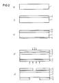
- the beam shape diaphragm shown schematically in FIG. 1, for an electron or ion beam recorder essentially consists of a semiconductor body 1, on the surface of which a silicon layer 2 has been epitaxially deposited.
- the epitaxial layer 2 which is designed as a self-supporting membrane in the central region, has a preferably line-shaped arrangement of square recesses 14 with vertical boundary surfaces. If a primary particle beam 15 is applied to this membrane, a large number of particle probes 16 are obtained on the side facing away from the particle source, the beam cross section of which is predetermined by the geometry of the recesses 14.
- the particle probes 16 can then be individually deflected or blanked using the known aperture diaphragm and mapped onto the object to be structured with the aid of a particle-optical unit.
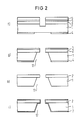
- the process for producing such a beam-shaped diaphragm comprises the following process steps (see FIG. 2): - Epitaxial deposition of a semiconductor layer 2, for example a silicon layer, on a semiconductor substrate 1 of a first conductivity type, for example p-doped silicon with (1, 0, 0) or (1, 1, 0) orientation (FIGS. 2a, b). - Doping the epitaxial layer 2 with boron (protection of the epitaxial layer 2 during later etching processes) and germanium (reduction of the mechanical stresses), the boron concentration should exceed 1 x 10²⁰ boron atoms / cm3 (the doping is preferably carried out during the epitaxial deposition).
- the beam shape diaphragm shown schematically in FIG. 1 can also be produced in low-doped epitaxial or diffusion layers using electrochemical etching processes.
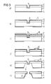
- the manufacturing process then comprises the following process steps (see Figure 3): - Epitaxial deposition of an n-doped silicon layer 2 on a semiconductor substrate 1, for example p-doped silicon (1, 0, 0) or (1, 1, 0) orientation (FIGS. 3a, b). - Coating the front of the wafer (epitaxial layer 2) and the back of the wafer (semiconductor substrate 1) with a dielectric 3 or 4, for example silicon nitride or silicon oxide (Figure 3c).
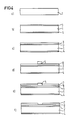
- the beam shape diaphragm can also be produced by using lithographic processes and galvanic molding.
- the manufacturing process then comprises the following process steps (see Figure 4): - Coating on both sides of a semiconductor substrate 1, for example silicon with (1, 0, 0) or (1, 1, 0) orientation, with a dielectric 3 or 4, for example silicon oxide or silicon nitride (FIGS. 4a, b).
- a dielectric 3 or 4 for example silicon oxide or silicon nitride
- an electroplating start layer 8 for example a chrome / gold or titanium / gold layer, on the front of the wafer (FIG. 4c).
- - Lithographic transfer of the geometry and arrangement of the recesses 14 to a photoresist layer 5 spun onto the electroplating start layer 8 (FIG. 4d).
Abstract
Description
Die Erfindung bezieht sich auf ein Verfahren zur Herstellung einer Strahlformblende für ein Lithographiegerät nach dem Oberbegriff des Patentanspruchs 1.The invention relates to a method for producing a beam shaping diaphragm for a lithography device according to the preamble of claim 1.
Aus der US-A-4 724 328 ist ein Lithographiegerät (Elektronenstrahlschreiber) bekannt, dessen elektronenoptische Säule eine Aperturblende zur Erzeugung einer Vielzahl individuell ablenkbarer Elektronensonden aufweist. Die in der EP-O 191 439 Al näher beschriebene Aperturblende besteht aus einer mit einer zeilenförmigen Mehrlochstruktur versehenen Siliziummembran, auf deren Oberfläche ein als Ablenkeinheit wirkendes Elektrodensystem angeordnet ist.A lithography device (electron beam recorder) is known from US Pat. No. 4,724,328, the electron-optical column of which has an aperture diaphragm for producing a large number of individually deflectable electron probes. The aperture diaphragm described in more detail in EP-O 191 439 A1 consists of a silicon membrane provided with a line-shaped multi-hole structure, on the surface of which an electrode system acting as a deflection unit is arranged.
Der Erfindung liegt die Aufgabe zugrunde, ein Verfahren zur Herstellung einer Strahlformblende für ein Lithographiegerät anzugeben, wobei die mit einem primären Teilchenstrahl beaufschlagte Blende eine Halbleitermembran mit Ausnehmungen zur Erzeugung einer Vielzahl von Teilchensonden aufweist. Diese Aufgabe wird erfindungsgemäß durch die Verfahren nach den Patentansprüchen 1, 2 und 3 gelöst. Die Unteransprüche betreffen vorteilhafte Weiterbildungen der erfindungsgemäßen Verfahren.The invention is based on the object of specifying a method for producing a beam-shaped diaphragm for a lithography device, the diaphragm having a primary particle beam having a semiconductor membrane with recesses for producing a multiplicity of particle probes. This object is achieved according to the invention by the method according to
Der mit der Erfindung erzielbare Vorteil besteht insbesondere darin, daß die den Strahlquerschnitt der Teilchensonden definierenden Ausnehmungen mit hoher Genauigkeit erzeugt werden können.The advantage that can be achieved with the invention is, in particular, that the recesses defining the beam cross section of the particle probes can be produced with high accuracy.
Die Erfindung wird im folgenden anhand der Zeichnungen näher erläutert. Hierbei zeigt
- Figur 1 den schematischen Aufbau der herzustellenden Strahlformblende,
Figur 2 bis 4 verschiedene Prozeßfolgen zur Herstellung der Strahlformblende.
- FIG. 1 shows the schematic structure of the beam shape diaphragm to be produced,
- Figure 2 to 4 different process sequences for the production of the beam aperture.
Die in Figur 1 schematisch dargestellte Strahlformblende für einen Elektronen- oder Ionenstrahlschreiber besteht im wesentlichen aus einem Halbleiterkörper 1, auf dessen Oberfläche eine Siliziumschicht 2 epitaktisch abgeschieden wurde. Die im mittleren Bereich als freitragende Membran ausgebildete Epitaxieschicht 2 besitzt eine vorzugsweise zeilenförmige Anordnung quadratischer Ausnehmungen 14 mit senkrechten Begrenzungsflächen. Wird diese Membran mit einem primären Teilchenstrahl 15 beaufschlagt, so erhält man auf der der Teilchenquelle abgewandten Seite eine Vielzahl von Teilchensonden 16, deren Strahlquerschnitt durch die Geometrie der Ausnehmungen 14 vorgegeben ist. Die Teilchensonden 16 können anschließend unter Verwendung der bekannten Aperturblende individuell abgelenkt bzw. ausgetastet und mit Hilfe einer teilchenoptischen Einheit auf das zu strukturierende Objekt abgebildet werden.The beam shape diaphragm, shown schematically in FIG. 1, for an electron or ion beam recorder essentially consists of a semiconductor body 1, on the surface of which a
Der Prozeß zur Herstellung einer solchen Strahlformblende umfaßt erfindungsgemäß die folgenden Verfahrensschritte (siehe Figur 2):
- Epitaktische Abscheidung einer Halbleiterschicht 2, beispielsweise einer Siliziumschicht, auf einem Halbleitersubstrat 1 eines ersten Leitfähigkeitstyps, beispielsweise p-dotiertes Silizium mit (1, 0, 0)- oder (1, 1, 0)-Orientierung (Figur 2a, b).
- Dotierung der Epitaxieschicht 2 mit Bor (Schutz der Epitaxieschicht 2 während späterer Ätzprozesse) und Germanium (Minderung der mechanischen Spannungen), wobei die Borkonzentration 1 x 10²⁰ Boratome/cm³ übersteigen sollte (die Dotierung wird vorzugsweise während der epitaktischen Abscheidung vorgenommen).
- Beschichtung der Wafervorderseite (Epitaxieschicht 2) und der Waferrückseite (Halbleitersubstrat 1) mit einem Dielektrikum 3 bzw. 4, beispielsweise Siliziumnitrid oder Siliziumoxid (Figur 2c).
- Lithographische Übertragung der Geometrie und Anordnung der Ausnehmungen 14 und der im Halbleitersubstrat 1 zu erzeugenden Durchgangsöffnung 17 auf die auf die Wafervorderseite bzw. Waferrückseite aufgeschleuderten Photolackschichten 5 bzw. 6 (Figur 2d).
- Reaktives Trockenätzen der dieleketrischen Schichten 2 und 4 (Strukturierung der Schichten 3 bzw. 4, Figur 2e).
- Reaktives Trockenätzen, insbesondere reaktives Ionenstrahlätzen der Epitaxieschicht 2 (Durchstossen der Epitaxieschicht; Figur 2f).
- Naßchemisches anisotropes Ätzen des Halbleitersubstrats 1 auf der Waferrückseite (Figur 2g).
- Entfernen der dielektrischen Schichten 3 und 4 (Figur 2h).
- Beschichtung der Epitaxieschicht 2 und des Halbleitersubstrats 1 mit einem Metall 6, beispielsweise Gold (Figur 2e).According to the invention, the process for producing such a beam-shaped diaphragm comprises the following process steps (see FIG. 2):
- Epitaxial deposition of a
- Doping the
- Coating the front of the wafer (epitaxial layer 2) and the back of the wafer (semiconductor substrate 1) with a dielectric 3 or 4, for example silicon nitride or Silicon oxide (Figure 2c).
- Lithographic transfer of the geometry and arrangement of the
- Reactive dry etching of the
- Reactive dry etching, in particular reactive ion beam etching of the epitaxial layer 2 (puncturing the epitaxial layer; FIG. 2f).
- Wet chemical anisotropic etching of the semiconductor substrate 1 on the back of the wafer (FIG. 2g).
- Removal of the dielectric layers 3 and 4 (Figure 2h).
- Coating the
Gemäß weiterer Erfindung kann die in Figur 1 schematisch dargestellte Strahlformblende auch in niedrig dotierten Epitaxie- oder Diffusionsschichten unter Anwendung elektrochemischer Ätzverfahren erzeugt werden. Der Herstellungsprozeß umfaßt dann die folgenden Verfahrensschritte (siehe Figur 3):
- Epitaktische Abscheidung einer n-dotierten Siliziumschicht 2 auf einem Halbleitersubstrat 1, beispielsweise p-dotiertes Silizium (1, 0, 0)- oder (1, 1, 0)-Orientierung (Figur 3a, b).
- Beschichtung der Wafervorderseite (Epitaxieschicht 2) und der Waferrückseite (Halbleitersubstrat 1) mit einem Dielektrikum 3 bzw. 4, beispielsweise Siliziumnitrid oder Siliziumoxid (Figur 3c).
- Lithographische Übertragung der Geometrie und Anordnung der Ausnehmungen 14 auf eine auf die dielektrische Schicht 3 aufgeschleuderte Photolackschicht 5 (Figur 3d).
- Reaktives Trockenätzen der dielektrischen Schicht 3, (Strukturierung der dielektrischen Schicht 3; Figur 3e).
- Anisotropes Trockenätzen der Epitaxieschicht 2 (Durchstossen der Epitaxieschicht 2; Figur 3f).
- Entfernen der Photolackschicht 5 und Abscheidung einer Passivierungsschicht 9 innerhalb der Ätzgruben bzw. Oxidation der durch den Ätzprozeß freigelegten Flächen (Figur 3g).
- Lithographische Erzeugung eines Kontaktfensters 10 in der dielektrischen Schicht 3 (Figur 3h).
- Lithographische Übertragung der Geometrie der Substratdurchgangsöffnung 17 auf eine auf die dielektrische Schicht 4 aufgeschleuderte Photolackschicht und Strukturierung der Schicht 4 (Figur 3h).
- Metallisierung der Wafervorderseite, beispielsweise mit einer Haftschicht aus Chrom oder Titan und einer Goldschicht 11 (Figur 3i).
- Lithographische Strukturierung der Metallisierung 11 zur Erzeugung eines elektrischen Kontaktes 12 (Figur 3j).
- Anisotropes Ätzes des Halbleitersubstrats 1, beispielsweise in KOH, unter Verwendung eines elektrochemischen Ätzstops, wobei die Epitaxieschicht 2 über den Kontakt 12 mit dem positiven Pol einer Spannungsquelle verbunden ist (Figur 3k).
- Entfernen des Kontaktes 12 und der dielektrischen Schich ten 3, 4 und 9.
- Beschichtung des Substrats 1 und der Epitaxieschicht 2 mit einem Metall 7, beispielsweise Gold (Figur 31).According to a further invention, the beam shape diaphragm shown schematically in FIG. 1 can also be produced in low-doped epitaxial or diffusion layers using electrochemical etching processes. The manufacturing process then comprises the following process steps (see Figure 3):
- Epitaxial deposition of an n-doped
- Coating the front of the wafer (epitaxial layer 2) and the back of the wafer (semiconductor substrate 1) with a dielectric 3 or 4, for example silicon nitride or silicon oxide (Figure 3c).
- Lithographic transfer of the geometry and arrangement of the
- Reactive dry etching of the dielectric layer 3 (structuring of the dielectric layer 3; FIG. 3e).
- Anisotropic dry etching of the epitaxial layer 2 (puncturing the
- Removal of the
- Lithographic generation of a
- Lithographic transfer of the geometry of the substrate passage opening 17 to a photoresist layer spun onto the dielectric layer 4 and structuring of the layer 4 (FIG. 3h).
- Metallization of the front of the wafer, for example with an adhesive layer made of chrome or titanium and a gold layer 11 (Figure 3i).
- Lithographic structuring of the metallization 11 to produce an electrical contact 12 (Figure 3j).
- Anisotropic etching of the semiconductor substrate 1, for example in KOH, using an electrochemical etching stop, the
- Remove the contact 12 and the dielectric layer ten 3, 4 and 9.
- Coating the substrate 1 and the
Gemäß weiterer Erfindung kann die Strahlformblende auch durch Anwendung lithographischer Verfahren und galvanische Abformung erzeugt werden. Der Herstellungsprozeß umfaßt dann die folgenden Verfahrensschritte (siehe Figur 4):
- Beidseitiges Beschichten eines Halbleitersubstrats 1, beispielsweise Silizium mit (1, 0, 0)- oder (1, 1, 0)-Orientierung, mit einem Dielektrikum 3 bzw. 4, beispielsweise Siliziumoxid oder Siliziumnitrid (Figur 4a, b).
- Aufbringen einer Galvanik-Startschicht 8, beispielsweise einer Chrom/Gold- oder Titan/Gold-Schicht, auf der Wafervorderseite (Figur 4c).
- Lithographische Übertragung der Geometrie und Anordnung der Ausnehmungen 14 auf eine auf die Galvanik-Startschicht 8 aufgeschleuderte Photolackschicht 5 (Figur 4d).
- Galvanische Abscheidung einer metallischen Schicht 7, insbesondere einer Goldschicht, auf der Wafervorderseite (Figur 4e).
- Entfernen der Photolackschicht 5 (Figur 4f).
- Lithographische Strukturierung der Passivierungsschicht 4 entsprechend der Geometrie der im Halbleitersubstrat 1 zu erzeugenden Durchgangsöffnung 17 (Figur 4g).
- Anisotropes naßchemisches Ätzen des Halbleitersubstrats 1 auf der Waferrückseite (Figur 4h).
- Ätzen der Passivierungsschicht 3 und der Galvanik-Startschicht 8 im Bereich der Substratdurchgangsöffnung 17 (Figur 4e).According to a further invention, the beam shape diaphragm can also be produced by using lithographic processes and galvanic molding. The manufacturing process then comprises the following process steps (see Figure 4):
- Coating on both sides of a semiconductor substrate 1, for example silicon with (1, 0, 0) or (1, 1, 0) orientation, with a dielectric 3 or 4, for example silicon oxide or silicon nitride (FIGS. 4a, b).
- Application of an
- Lithographic transfer of the geometry and arrangement of the
- Galvanic deposition of a
- Remove the photoresist layer 5 (Figure 4f).
- Lithographic structuring of the passivation layer 4 in accordance with the geometry of the through
- Anisotropic wet chemical etching of the semiconductor substrate 1 on the back of the wafer (FIG. 4h).
- Etching of the passivation layer 3 and the
Claims (5)
- daß eine Halbleiterschicht (2) eines ersten Leitfähigkeitstyps auf einem Halbleitersubstrat (1) eines zweiten Leitfähigkeitstyps abgeschieden wird,
- daß die Halbleiterschicht (2) mit einer ersten dielektrischen Schicht (3) und das Halbleitersubstrat (1) rückseitig mit einer zweiten dielektrischen Schicht (4) versehen wird,
- daß die erste dielektrische Schicht (3) entsprechend der Geometrie und Anordnung der zu erzeugenden Ausnehmungen (14) strukturiert wird,
- daß die zweite dielektrische Schicht (4) entsprechend der Geometrie einer im Halbleitersubstrat (1) zu erzeugenden Durchgangsöffnung (17) strukturiert wird,
- daß die Halbleiterschicht (2) in einem Ätzprozeß durchstossen wird,
- daß die Durchgangsöffnungen (17) durch anisotropes Ätzen des Halbleitersubstrats (1) erzeugt wird,
- daß die dielektrischen Schichten (3, 4) entfernt werden
- und daß die Halbleiterschicht (2) und das Halbleitersubstrat (1) mit einer Metallisierung (7) versehen werden.1. A method for producing a beam-shaped diaphragm for a lithography device, the beam-shaped diaphragm having a primary particle beam (15) having a semiconductor membrane (2) with recesses (14) for producing a multiplicity of particle probes (16), characterized in that
- that a semiconductor layer (2) of a first conductivity type is deposited on a semiconductor substrate (1) of a second conductivity type,
- That the semiconductor layer (2) with a first dielectric layer (3) and the semiconductor substrate (1) is provided on the back with a second dielectric layer (4),
- That the first dielectric layer (3) is structured according to the geometry and arrangement of the recesses (14) to be produced,
- That the second dielectric layer (4) is structured according to the geometry of a through opening (17) to be produced in the semiconductor substrate (1),
- That the semiconductor layer (2) is pierced in an etching process,
- That the through openings (17) is produced by anisotropic etching of the semiconductor substrate (1),
- That the dielectric layers (3, 4) are removed
- And that the semiconductor layer (2) and the semiconductor substrate (1) are provided with a metallization (7).
- daß eine Halbleiterschicht (2) eines ersten Leitfähigkeitstyps auf einem Halbleitersubstrat (1) eines zweiten Leitfähigkeitstyps abgeschieden wird,
- daß die Halbleiterschicht (2) mit einer ersten dielektrischen Schicht (3) und das Halbleitersubstrat (1) mit einer zweiten dielektrischen Schicht (4) versehen wird,
- daß die erste dielektrische Schicht (3) entsprechend der Geometrie und Anordnung der zu erzeugenden Ausnehmungen (14) strukturiert wird,
- daß die Halbleiterschicht (2) in einem Ätzprozeß durchstossen wird,
- daß eine Passivierungsschicht (9) innerhalb der Ätzgruben abgeschieden wird,
- daß ein Fenster (10) in der ersten dielektrischen Schicht (3) erzeugt wird,
- daß die zweite dielektrische Schicht (4) entsprechend der Geometrie einer im Halbleitersubstrat (1) zu erzeugenden Durchgangsöffnung (17) strukturiert wird,
- daß die erste dielektrische Schicht (3) mit einer ersten Metallschicht (11) versehen wird,
- daß ein elektrischer Kontakt (12) durch lithographische Strukturierung der ersten metallischen Schicht (11) erzeugt wird,
- daß die Durchgangsöffnung (17) durch anisotropes Ätzen des Halbleitersubstrats (1) unter Verwendung eines elek trochemischen Ätzstops erzeugt wird, wobei die Halbleiterschicht (2) über den elektrischen Kontakt (12) mit einem Pol einer Spannungsquelle verbunden ist,
- daß die dielektrischen Schichten (3, 4) und der elektrische Kontakt (12) entfernt werden,
- und daß die Halbleiterschicht (2) und das Halbleitersubstrat (1) mit einer zweiten metallischen Schicht (7) versehen werden.2. A method for producing a beam aperture for a lithography device, which with a primary particle beam (15) acted upon beam shape diaphragm has a semiconductor membrane (2) with recesses (14) for producing a plurality of particle probes (16), characterized in that
- that a semiconductor layer (2) of a first conductivity type is deposited on a semiconductor substrate (1) of a second conductivity type,
- That the semiconductor layer (2) is provided with a first dielectric layer (3) and the semiconductor substrate (1) with a second dielectric layer (4),
- That the first dielectric layer (3) is structured according to the geometry and arrangement of the recesses (14) to be produced,
- That the semiconductor layer (2) is pierced in an etching process,
- that a passivation layer (9) is deposited within the etching pits,
- That a window (10) is generated in the first dielectric layer (3),
- That the second dielectric layer (4) is structured according to the geometry of a through opening (17) to be produced in the semiconductor substrate (1),
- That the first dielectric layer (3) is provided with a first metal layer (11),
- That an electrical contact (12) is generated by lithographic structuring of the first metallic layer (11),
- That the through hole (17) by anisotropic etching of the semiconductor substrate (1) using an elec trochemical etching stops are produced, the semiconductor layer (2) being connected to a pole of a voltage source via the electrical contact (12),
- That the dielectric layers (3, 4) and the electrical contact (12) are removed,
- And that the semiconductor layer (2) and the semiconductor substrate (1) are provided with a second metallic layer (7).
- daß ein Halbleiterkörper (1) vorderseitig mit einer ersten dielektrischen Schicht (3) und rückseitig mit einer zweiten dielektrischen Schicht (4) versehen wird,
- daß eine erste metallische Schicht (8) auf der ersten dielektrischen Schicht (3) aufgebracht wird,
- daß die Geometrie und Anordnung der zu erzeugenden Ausnehmungen (14) auf eine auf die erste metallische Schicht (8) aufgebrachte Photolackschicht (5) übertragen wird,
- daß eine zweite metallische Schicht (7) auf der ersten metallischen Schicht (8) galvanisch abgeschieden wird,
- daß die Photolackschicht (5) entfernt wird,
- daß die zweite dielektrische Schicht (4) entsprechend der Geometrie einer im Halbleitersubstrat (1) zu erzeugenden Durchgangsöffnung (17) strukturiert wird,
- daß das Halbleitersubstrat (1) einem anisotropen Ätzpro zeß unterworfen wird,
- und daß die erste dielektrische Schicht (3) und die ersten metallischen Schicht (8) im Bereich der Durchgangsöffnung (17) entfernt werden.3. A method for producing a beam-shaped diaphragm for a lithography device, the beam-shaped diaphragm having a primary particle beam (15) having a semiconductor membrane (2) with recesses (14) for producing a multiplicity of particle probes (16), characterized in that
- That a semiconductor body (1) is provided on the front side with a first dielectric layer (3) and on the rear side with a second dielectric layer (4),
- That a first metallic layer (8) is applied to the first dielectric layer (3),
- That the geometry and arrangement of the recesses (14) to be produced is transferred to a photoresist layer (5) applied to the first metallic layer (8),
- That a second metallic layer (7) is electrodeposited on the first metallic layer (8),
- That the photoresist layer (5) is removed,
- That the second dielectric layer (4) is structured according to the geometry of a through opening (17) to be produced in the semiconductor substrate (1),
- That the semiconductor substrate (1) an anisotropic Ätzpro is subjected to
- And that the first dielectric layer (3) and the first metallic layer (8) in the region of the through opening (17) are removed.
Applications Claiming Priority (2)
| Application Number | Priority Date | Filing Date | Title |
|---|---|---|---|
| DE3818536 | 1988-05-31 | ||
| DE3818536 | 1988-05-31 |
Publications (2)
| Publication Number | Publication Date |
|---|---|
| EP0344515A2 true EP0344515A2 (en) | 1989-12-06 |
| EP0344515A3 EP0344515A3 (en) | 1991-01-30 |
Family
ID=6355538
Family Applications (1)
| Application Number | Title | Priority Date | Filing Date |
|---|---|---|---|
| EP19890108869 Withdrawn EP0344515A3 (en) | 1988-05-31 | 1989-05-17 | Process for producing a beam-forming aperture for a lithography apparatus |
Country Status (3)
| Country | Link |
|---|---|
| US (1) | US5049460A (en) |
| EP (1) | EP0344515A3 (en) |
| JP (1) | JPH0251832A (en) |
Cited By (3)
| Publication number | Priority date | Publication date | Assignee | Title |
|---|---|---|---|---|
| EP0565069A1 (en) * | 1992-04-10 | 1993-10-13 | Fraunhofer-Gesellschaft Zur Förderung Der Angewandten Forschung E.V. | Adjustable diaphragm and manufacturing process |
| CN104599927A (en) * | 2014-12-24 | 2015-05-06 | 西安理工大学 | Preparation method for porous diaphragm |
| US9824860B2 (en) | 2014-02-26 | 2017-11-21 | Advantest Corp. | Charged particle beam exposure apparatus and method of manufacturing semiconductor device |
Families Citing this family (8)
| Publication number | Priority date | Publication date | Assignee | Title |
|---|---|---|---|---|
| ZA944488B (en) * | 1993-06-23 | 1995-02-15 | New York Blood Center Inc | System for viral inactivation of blood |
| EP0791459B1 (en) * | 1996-02-22 | 2002-05-22 | Seiko Epson Corporation | Ink-jet recording head, ink-jet recording apparatus using the same, and method for producing ink-jet recording head |
| US6528340B2 (en) * | 2001-01-03 | 2003-03-04 | Honeywell International Inc. | Pressure transducer with composite diaphragm |
| JP2002237441A (en) * | 2001-02-08 | 2002-08-23 | Advantest Corp | Method of manufacturing slit, slit, and electron-beam exposure apparatus |
| JP3951613B2 (en) * | 2001-02-09 | 2007-08-01 | 株式会社ケンウッド | Microphone |
| US20040104454A1 (en) * | 2002-10-10 | 2004-06-03 | Rohm Co., Ltd. | Semiconductor device and method of producing the same |
| JP6212000B2 (en) * | 2014-07-02 | 2017-10-11 | 株式会社東芝 | Pressure sensor, and microphone, blood pressure sensor, and touch panel using pressure sensor |
| CN113228220A (en) * | 2018-12-26 | 2021-08-06 | Asml荷兰有限公司 | Method for manufacturing aperture device |
Citations (4)
| Publication number | Priority date | Publication date | Assignee | Title |
|---|---|---|---|---|
| JPS6081750A (en) * | 1983-10-11 | 1985-05-09 | Nec Corp | Aperture diaphragm and its manufacturing method |
| JPS6119040A (en) * | 1984-07-05 | 1986-01-27 | Nec Corp | Manufacture of aperture diaphragm |
| EP0191439A1 (en) * | 1985-02-12 | 1986-08-20 | Siemens Aktiengesellschaft | Linearly structured multiple aperture and beam blanking electrodes for the production of a multiplicity of individually blankable corpuscular beam probes in a lithography apparatus |
| EP0221657A1 (en) * | 1985-09-27 | 1987-05-13 | AT&T Corp. | Charged-particle-beam lithography |
Family Cites Families (6)
| Publication number | Priority date | Publication date | Assignee | Title |
|---|---|---|---|---|
| DE2922416A1 (en) * | 1979-06-01 | 1980-12-11 | Ibm Deutschland | SHADOW MASK FOR STRUCTURING SURFACE AREAS AND METHOD FOR THEIR PRODUCTION |
| DE3176643D1 (en) * | 1981-10-30 | 1988-03-10 | Ibm Deutschland | Shadow projecting mask for ion implantation and lithography by ion beam radiation |
| DE3425063A1 (en) * | 1984-07-07 | 1986-02-06 | Licentia Patent-Verwaltungs-Gmbh, 6000 Frankfurt | MASK FOR X-RAY LITHOGRAPHY |
| DE3504714A1 (en) * | 1985-02-12 | 1986-08-14 | Siemens AG, 1000 Berlin und 8000 München | LITHOGRAPH DEVICE FOR GENERATING MICROSTRUCTURES |
| DE3677005D1 (en) * | 1986-05-06 | 1991-02-21 | Ibm Deutschland | MASK FOR ION, ELECTRON OR X-RAY RAY LITHOGRAPHY AND METHOD FOR THE PRODUCTION THEREOF. |
| US4932872A (en) * | 1989-06-16 | 1990-06-12 | Lepton Inc. | Method for fabricating X-ray masks |
-
1989
- 1989-05-17 US US07/353,062 patent/US5049460A/en not_active Expired - Fee Related
- 1989-05-17 EP EP19890108869 patent/EP0344515A3/en not_active Withdrawn
- 1989-05-29 JP JP1137320A patent/JPH0251832A/en active Pending
Patent Citations (4)
| Publication number | Priority date | Publication date | Assignee | Title |
|---|---|---|---|---|
| JPS6081750A (en) * | 1983-10-11 | 1985-05-09 | Nec Corp | Aperture diaphragm and its manufacturing method |
| JPS6119040A (en) * | 1984-07-05 | 1986-01-27 | Nec Corp | Manufacture of aperture diaphragm |
| EP0191439A1 (en) * | 1985-02-12 | 1986-08-20 | Siemens Aktiengesellschaft | Linearly structured multiple aperture and beam blanking electrodes for the production of a multiplicity of individually blankable corpuscular beam probes in a lithography apparatus |
| EP0221657A1 (en) * | 1985-09-27 | 1987-05-13 | AT&T Corp. | Charged-particle-beam lithography |
Non-Patent Citations (2)
| Title |
|---|
| PATENT ABSTRACTS OF JAPAN, Band 10, Nr. 168 (E-411)[2224], 14. Juni 1986; & JP-A-61 019 040 (NIPPON DENKI K.K.) 27-01-1986 * |
| PATENT ABSTRACTS OF JAPAN, Band 9, Nr. 219 (M-410)[1942], 6. September 1985; & JP-A-60 081 750 (NIPPON DENKI K.K.) 09-05-1985 * |
Cited By (5)
| Publication number | Priority date | Publication date | Assignee | Title |
|---|---|---|---|---|
| EP0565069A1 (en) * | 1992-04-10 | 1993-10-13 | Fraunhofer-Gesellschaft Zur Förderung Der Angewandten Forschung E.V. | Adjustable diaphragm and manufacturing process |
| US9824860B2 (en) | 2014-02-26 | 2017-11-21 | Advantest Corp. | Charged particle beam exposure apparatus and method of manufacturing semiconductor device |
| DE102014114081B4 (en) | 2014-02-26 | 2018-04-05 | Advantest Corporation | A charged particle beam exposure apparatus and method of manufacturing a semiconductor device |
| CN104599927A (en) * | 2014-12-24 | 2015-05-06 | 西安理工大学 | Preparation method for porous diaphragm |
| CN104599927B (en) * | 2014-12-24 | 2016-11-30 | 西安理工大学 | A kind of preparation method of porous diaphragm |
Also Published As
| Publication number | Publication date |
|---|---|
| US5049460A (en) | 1991-09-17 |
| EP0344515A3 (en) | 1991-01-30 |
| JPH0251832A (en) | 1990-02-21 |
Similar Documents
| Publication | Publication Date | Title |
|---|---|---|
| DE19954022B4 (en) | Semiconductor physical quantity sensor and method of making the same | |
| EP0048291B1 (en) | Structure with a silicon body that presents an aperture and method of making this structure | |
| DE4310206C2 (en) | Method for producing a solar cell from a substrate wafer | |
| DE2801338C2 (en) | Process for the production of electrodes made of different metals for semiconductor components of small dimensions | |
| DE102005040267B4 (en) | Method for producing a multilayer electrostatic lens arrangement, in particular a phase plate and such a phase plate | |
| EP0344515A2 (en) | Process for producing a beam-forming aperture for a lithography apparatus | |
| WO1995005008A2 (en) | Flat component with a grid of through holes | |
| US4338164A (en) | Method for producing planar surfaces having very fine peaks in the micron range | |
| DE3504705A1 (en) | APERTURE DISPLAY WITH CELL-SHAPED MULTIPLE HOLE STRUCTURE AND PUSHING ELECTRODES FOR THE GENERATION OF A MULTIPLE OF INDIVIDUALLY TESTABLE BODY BEAM PROBE FOR A LITHOGRAPH DEVICE | |
| EP0367750A2 (en) | Process for producing a silicon membrane with controlled mechanical stress | |
| WO2009006988A1 (en) | Contact structure for a semiconductor component and a method for production thereof | |
| EP0344513A2 (en) | Process for the manufacture of a steering plate for a lithography apparatus | |
| DE19708766C2 (en) | Lithography mask and method of making the same | |
| DE69723209T2 (en) | Electron tube with an electron multiplier | |
| DE3703516A1 (en) | METHOD AND DEVICE FOR ALIGNMENT | |
| DE19527314A1 (en) | Fabrication of silicon membrane with predefined parameters | |
| EP0154796B1 (en) | Manufacturing process for layered metallic multichannel plates for an image intensifier, and use of plates so manufactured | |
| WO2018219591A1 (en) | Method for producing a fuel cell and a fuel cell | |
| EP1495497B1 (en) | Position-sensitive germanium detectors having a microstructure on both contact surfaces | |
| DE19755990C1 (en) | Atom probe extraction electrode manufacturing method | |
| DE2843310C2 (en) | Method and device for processing a semiconductor wafer with the dissipation of charge accumulations which occur in an electrically conductive region of the semiconductor wafer as a result of exposure to radiation | |
| EP0973027B1 (en) | Method for manufacturing an electrode | |
| EP1399977A2 (en) | Dual-sided microstructured, position-sensitive detector | |
| DD206924A3 (en) | METHOD FOR PRODUCING A FREE-SPACING DISTANCE MASK | |
| DE10143096A1 (en) | Electron beam exposure device, component for forming a corpuscular beam and method for producing this component |
Legal Events
| Date | Code | Title | Description |
|---|---|---|---|
| PUAI | Public reference made under article 153(3) epc to a published international application that has entered the european phase |
Free format text: ORIGINAL CODE: 0009012 |
|
| AK | Designated contracting states |
Kind code of ref document: A2 Designated state(s): DE FR GB NL |
|
| PUAL | Search report despatched |
Free format text: ORIGINAL CODE: 0009013 |
|
| 17P | Request for examination filed |
Effective date: 19901205 |
|
| AK | Designated contracting states |
Kind code of ref document: A3 Designated state(s): DE FR GB NL |
|
| 17Q | First examination report despatched |
Effective date: 19930824 |
|
| STAA | Information on the status of an ep patent application or granted ep patent |
Free format text: STATUS: THE APPLICATION IS DEEMED TO BE WITHDRAWN |
|
| 18D | Application deemed to be withdrawn |
Effective date: 19931201 |