EP0344515A2 - Procédé de fabrication d'un diaphragme de mise en forme du faisceau pour un appareil de lithographie - Google Patents
Procédé de fabrication d'un diaphragme de mise en forme du faisceau pour un appareil de lithographie Download PDFInfo
- Publication number
- EP0344515A2 EP0344515A2 EP89108869A EP89108869A EP0344515A2 EP 0344515 A2 EP0344515 A2 EP 0344515A2 EP 89108869 A EP89108869 A EP 89108869A EP 89108869 A EP89108869 A EP 89108869A EP 0344515 A2 EP0344515 A2 EP 0344515A2
- Authority
- EP
- European Patent Office
- Prior art keywords
- layer
- semiconductor substrate
- semiconductor
- dielectric layer
- produced
- Prior art date
- Legal status (The legal status is an assumption and is not a legal conclusion. Google has not performed a legal analysis and makes no representation as to the accuracy of the status listed.)
- Withdrawn
Links
Images


Classifications
-
- H—ELECTRICITY
- H01—ELECTRIC ELEMENTS
- H01J—ELECTRIC DISCHARGE TUBES OR DISCHARGE LAMPS
- H01J9/00—Apparatus or processes specially adapted for the manufacture, installation, removal, maintenance of electric discharge tubes, discharge lamps, or parts thereof; Recovery of material from discharge tubes or lamps
- H01J9/02—Manufacture of electrodes or electrode systems
-
- H—ELECTRICITY
- H01—ELECTRIC ELEMENTS
- H01J—ELECTRIC DISCHARGE TUBES OR DISCHARGE LAMPS
- H01J37/00—Discharge tubes with provision for introducing objects or material to be exposed to the discharge, e.g. for the purpose of examination or processing thereof
- H01J37/02—Details
- H01J37/04—Arrangements of electrodes and associated parts for generating or controlling the discharge, e.g. electron-optical arrangement or ion-optical arrangement
- H01J37/09—Diaphragms; Shields associated with electron or ion-optical arrangements; Compensation of disturbing fields
Definitions
- the invention relates to a method for producing a beam shaping diaphragm for a lithography device according to the preamble of claim 1.
- a lithography device (electron beam recorder) is known from US Pat. No. 4,724,328, the electron-optical column of which has an aperture diaphragm for producing a large number of individually deflectable electron probes.
- the aperture diaphragm described in more detail in EP-O 191 439 A1 consists of a silicon membrane provided with a line-shaped multi-hole structure, on the surface of which an electrode system acting as a deflection unit is arranged.
- the invention is based on the object of specifying a method for producing a beam-shaped diaphragm for a lithography device, the diaphragm having a primary particle beam having a semiconductor membrane with recesses for producing a multiplicity of particle probes.
- This object is achieved according to the invention by the method according to patent claims 1, 2 and 3.
- the subclaims relate to advantageous developments of the method according to the invention.
- the advantage that can be achieved with the invention is, in particular, that the recesses defining the beam cross section of the particle probes can be produced with high accuracy.
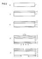
- the beam shape diaphragm shown schematically in FIG. 1, for an electron or ion beam recorder essentially consists of a semiconductor body 1, on the surface of which a silicon layer 2 has been epitaxially deposited.
- the epitaxial layer 2 which is designed as a self-supporting membrane in the central region, has a preferably line-shaped arrangement of square recesses 14 with vertical boundary surfaces. If a primary particle beam 15 is applied to this membrane, a large number of particle probes 16 are obtained on the side facing away from the particle source, the beam cross section of which is predetermined by the geometry of the recesses 14.
- the particle probes 16 can then be individually deflected or blanked using the known aperture diaphragm and mapped onto the object to be structured with the aid of a particle-optical unit.
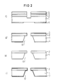
- the process for producing such a beam-shaped diaphragm comprises the following process steps (see FIG. 2): - Epitaxial deposition of a semiconductor layer 2, for example a silicon layer, on a semiconductor substrate 1 of a first conductivity type, for example p-doped silicon with (1, 0, 0) or (1, 1, 0) orientation (FIGS. 2a, b). - Doping the epitaxial layer 2 with boron (protection of the epitaxial layer 2 during later etching processes) and germanium (reduction of the mechanical stresses), the boron concentration should exceed 1 x 10²⁰ boron atoms / cm3 (the doping is preferably carried out during the epitaxial deposition).
- the beam shape diaphragm shown schematically in FIG. 1 can also be produced in low-doped epitaxial or diffusion layers using electrochemical etching processes.
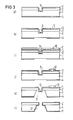
- the manufacturing process then comprises the following process steps (see Figure 3): - Epitaxial deposition of an n-doped silicon layer 2 on a semiconductor substrate 1, for example p-doped silicon (1, 0, 0) or (1, 1, 0) orientation (FIGS. 3a, b). - Coating the front of the wafer (epitaxial layer 2) and the back of the wafer (semiconductor substrate 1) with a dielectric 3 or 4, for example silicon nitride or silicon oxide (Figure 3c).
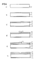
- the beam shape diaphragm can also be produced by using lithographic processes and galvanic molding.
- the manufacturing process then comprises the following process steps (see Figure 4): - Coating on both sides of a semiconductor substrate 1, for example silicon with (1, 0, 0) or (1, 1, 0) orientation, with a dielectric 3 or 4, for example silicon oxide or silicon nitride (FIGS. 4a, b).
- a dielectric 3 or 4 for example silicon oxide or silicon nitride
- an electroplating start layer 8 for example a chrome / gold or titanium / gold layer, on the front of the wafer (FIG. 4c).
- - Lithographic transfer of the geometry and arrangement of the recesses 14 to a photoresist layer 5 spun onto the electroplating start layer 8 (FIG. 4d).
Landscapes
- Chemical & Material Sciences (AREA)
- Analytical Chemistry (AREA)
- Engineering & Computer Science (AREA)
- Manufacturing & Machinery (AREA)
- Electron Beam Exposure (AREA)
- Micromachines (AREA)
Applications Claiming Priority (2)
| Application Number | Priority Date | Filing Date | Title |
|---|---|---|---|
| DE3818536 | 1988-05-31 | ||
| DE3818536 | 1988-05-31 |
Publications (2)
| Publication Number | Publication Date |
|---|---|
| EP0344515A2 true EP0344515A2 (fr) | 1989-12-06 |
| EP0344515A3 EP0344515A3 (fr) | 1991-01-30 |
Family
ID=6355538
Family Applications (1)
| Application Number | Title | Priority Date | Filing Date |
|---|---|---|---|
| EP19890108869 Withdrawn EP0344515A3 (fr) | 1988-05-31 | 1989-05-17 | Procédé de fabrication d'un diaphragme de mise en forme du faisceau pour un appareil de lithographie |
Country Status (3)
| Country | Link |
|---|---|
| US (1) | US5049460A (fr) |
| EP (1) | EP0344515A3 (fr) |
| JP (1) | JPH0251832A (fr) |
Cited By (3)
| Publication number | Priority date | Publication date | Assignee | Title |
|---|---|---|---|---|
| EP0565069A1 (fr) * | 1992-04-10 | 1993-10-13 | Fraunhofer-Gesellschaft Zur Förderung Der Angewandten Forschung E.V. | Diaphragma adjustable et procédé de fabrication |
| CN104599927A (zh) * | 2014-12-24 | 2015-05-06 | 西安理工大学 | 一种多孔光阑的制备方法 |
| US9824860B2 (en) | 2014-02-26 | 2017-11-21 | Advantest Corp. | Charged particle beam exposure apparatus and method of manufacturing semiconductor device |
Families Citing this family (10)
| Publication number | Priority date | Publication date | Assignee | Title |
|---|---|---|---|---|
| KR960703167A (ko) * | 1993-06-23 | 1996-06-19 | 존 더블유. 아담슨 | 혈액내 바이러스 불활성화 시스템(system for viral inactivation of blood) |
| US6209992B1 (en) * | 1996-02-22 | 2001-04-03 | Seiko Epson Corporation | Ink-jet recording head, ink-jet recording apparatus using the same, and method for producing ink-jet recording head |
| US6528340B2 (en) * | 2001-01-03 | 2003-03-04 | Honeywell International Inc. | Pressure transducer with composite diaphragm |
| JP2002237441A (ja) * | 2001-02-08 | 2002-08-23 | Advantest Corp | スリット製造方法、スリット、及び電子ビーム露光装置 |
| JP3951613B2 (ja) * | 2001-02-09 | 2007-08-01 | 株式会社ケンウッド | マイクロホン |
| US20040104454A1 (en) * | 2002-10-10 | 2004-06-03 | Rohm Co., Ltd. | Semiconductor device and method of producing the same |
| JP6212000B2 (ja) * | 2014-07-02 | 2017-10-11 | 株式会社東芝 | 圧力センサ、並びに圧力センサを用いたマイクロフォン、血圧センサ、及びタッチパネル |
| US10879034B2 (en) * | 2017-06-21 | 2020-12-29 | King Abdullah University Of Science And Technology | Membraneless platform for correlated analysis of nanomaterials |
| KR102634208B1 (ko) * | 2018-12-26 | 2024-02-07 | 에이에스엠엘 네델란즈 비.브이. | 기판을 에칭하기 위한 시스템 및 방법 |
| CN119566747B (zh) * | 2025-02-08 | 2025-05-02 | 中国科学院地质与地球物理研究所 | 一种长寿型纳米离子探针光阑的制备方法 |
Family Cites Families (8)
| Publication number | Priority date | Publication date | Assignee | Title |
|---|---|---|---|---|
| DE2922416A1 (de) * | 1979-06-01 | 1980-12-11 | Ibm Deutschland | Schattenwurfmaske zum strukturieren von oberflaechenbereichen und verfahren zu ihrer herstellung |
| EP0078336B1 (fr) * | 1981-10-30 | 1988-02-03 | Ibm Deutschland Gmbh | Masque projetant l'ombre pour l'implantation d'ions et pour la lithographie par rayons d'ions |
| DE3425063A1 (de) * | 1984-07-07 | 1986-02-06 | Licentia Patent-Verwaltungs-Gmbh, 6000 Frankfurt | Maske fuer die roentgenlithographie |
| DE3504705A1 (de) * | 1985-02-12 | 1986-08-14 | Siemens AG, 1000 Berlin und 8000 München | Aperturblende mit zellenfoermiger mehrlochstruktur und austastelektroden zur erzeugung einer mehrzahl von individuell austastbaren korpuskularstrahlsonden fuer ein lithografiegeraet |
| DE3504714A1 (de) * | 1985-02-12 | 1986-08-14 | Siemens AG, 1000 Berlin und 8000 München | Lithografiegeraet zur erzeugung von mikrostrukturen |
| CN86105432A (zh) * | 1985-09-27 | 1987-05-27 | 美国电话电报公司 | 带电粒子束曝光 |
| EP0244496B1 (fr) * | 1986-05-06 | 1991-01-16 | Ibm Deutschland Gmbh | Masque pour lithographie avec des ions, des électrons ou avec des rayons X et procédé de fabrication |
| US4932872A (en) * | 1989-06-16 | 1990-06-12 | Lepton Inc. | Method for fabricating X-ray masks |
-
1989
- 1989-05-17 EP EP19890108869 patent/EP0344515A3/fr not_active Withdrawn
- 1989-05-17 US US07/353,062 patent/US5049460A/en not_active Expired - Fee Related
- 1989-05-29 JP JP1137320A patent/JPH0251832A/ja active Pending
Cited By (5)
| Publication number | Priority date | Publication date | Assignee | Title |
|---|---|---|---|---|
| EP0565069A1 (fr) * | 1992-04-10 | 1993-10-13 | Fraunhofer-Gesellschaft Zur Förderung Der Angewandten Forschung E.V. | Diaphragma adjustable et procédé de fabrication |
| US9824860B2 (en) | 2014-02-26 | 2017-11-21 | Advantest Corp. | Charged particle beam exposure apparatus and method of manufacturing semiconductor device |
| DE102014114081B4 (de) | 2014-02-26 | 2018-04-05 | Advantest Corporation | Ladungsteilchenstrahl-Belichtungsgerät und Verfahren zur Herstellung eines Halbleiterbauelements |
| CN104599927A (zh) * | 2014-12-24 | 2015-05-06 | 西安理工大学 | 一种多孔光阑的制备方法 |
| CN104599927B (zh) * | 2014-12-24 | 2016-11-30 | 西安理工大学 | 一种多孔光阑的制备方法 |
Also Published As
| Publication number | Publication date |
|---|---|
| JPH0251832A (ja) | 1990-02-21 |
| EP0344515A3 (fr) | 1991-01-30 |
| US5049460A (en) | 1991-09-17 |
Similar Documents
| Publication | Publication Date | Title |
|---|---|---|
| DE19954022B4 (de) | Halbleitersensor für eine physikalische Grösse und Verfahren zu dessen Herstellung | |
| EP0344515A2 (fr) | Procédé de fabrication d'un diaphragme de mise en forme du faisceau pour un appareil de lithographie | |
| EP0048291B1 (fr) | Structure comprenant un corps de silicium présentant une ouverture le traversant de part en part et procédé de fabrication | |
| DE4310206C2 (de) | Verfahren zur Herstellung einer Solarzelle aus einer Substratscheibe | |
| DE69801429T2 (de) | Verfahren zur herstellung von karten mit mehreren kontaktspitzen zum testen von halbleiterchips | |
| DE2801338C2 (de) | Verfahren zur Erzeugung von aus unterschiedlichen Metallen bestehenden Elektroden für Halbleiter-Bauelemente kleiner Dimension | |
| EP0553464B1 (fr) | Procédé de fabrication d'une cellule solaire à partir d'un substrat | |
| WO1995005008A2 (fr) | Element plat comportant un reseau quadrille de trous de passage | |
| DE102005040267B4 (de) | Verfahren zum Herstellen einer mehrschichtigen elektrostatischen Linsenanordnung, insbesondere einer Phasenplatte und derartige Phasenplatte | |
| DE2951287C2 (de) | Verfahren zur Herstellung von mit einer Vielzahl von feinsten Spitzen versehenen Oberflächen | |
| DE69723209T2 (de) | Elektronenröhre mit einem Elektronenvervielfacher | |
| DE3504705A1 (de) | Aperturblende mit zellenfoermiger mehrlochstruktur und austastelektroden zur erzeugung einer mehrzahl von individuell austastbaren korpuskularstrahlsonden fuer ein lithografiegeraet | |
| DE19732624A1 (de) | Fotodetektor und Verfahren zu dessen Herstellung | |
| EP2162922A1 (fr) | Structure de contact pour un composant semi-conducteur et son procédé de fabrication | |
| EP0344513A2 (fr) | Procédé de fabrication d'une plaque de commande pour un appareil de lithographie | |
| DE19708766A1 (de) | Lithographiemaske und Verfahren zur Herstellung derselben | |
| DE69401243T2 (de) | Feldemissionsvorrichtung mit Kleinradiuskathode und Herstellungsverfahren dieser Vorrichtung | |
| DE102017209031A1 (de) | Verfahren zur Herstellung einer Brennstoffzelle und Brennstoffzelle | |
| EP0154796B1 (fr) | Procédé de fabrication d'un empilement de plaques multicanaux métalliques pour intensificateur d'images et utilisation de plaques ainsi fabriquées | |
| EP0684618A2 (fr) | Procédé de fabrication d'un condensateur au silicium | |
| DE2643811C2 (de) | Lithographie-Maske mit einer für Strahlung durchlässigen Membran und Verfahren zu ihrer Herstellung | |
| EP0836540A1 (fr) | Procede pour la fabrication d'empreintes de moule | |
| DE102006007431A1 (de) | Durch Halbleitersilizium-Verfahrenstechnik gebildeter Probenträger | |
| EP0973027B1 (fr) | Procédé de fabrication d'une électrode | |
| DE19755990C1 (de) | Verfahren zur Herstellung von Extraktionselektroden für die Atom-Analytik |
Legal Events
| Date | Code | Title | Description |
|---|---|---|---|
| PUAI | Public reference made under article 153(3) epc to a published international application that has entered the european phase |
Free format text: ORIGINAL CODE: 0009012 |
|
| AK | Designated contracting states |
Kind code of ref document: A2 Designated state(s): DE FR GB NL |
|
| PUAL | Search report despatched |
Free format text: ORIGINAL CODE: 0009013 |
|
| 17P | Request for examination filed |
Effective date: 19901205 |
|
| AK | Designated contracting states |
Kind code of ref document: A3 Designated state(s): DE FR GB NL |
|
| 17Q | First examination report despatched |
Effective date: 19930824 |
|
| STAA | Information on the status of an ep patent application or granted ep patent |
Free format text: STATUS: THE APPLICATION IS DEEMED TO BE WITHDRAWN |
|
| 18D | Application deemed to be withdrawn |
Effective date: 19931201 |