EP0343683B1 - Générateur de données de commande pour un processeur de triage - Google Patents
Générateur de données de commande pour un processeur de triage Download PDFInfo
- Publication number
- EP0343683B1 EP0343683B1 EP89109538A EP89109538A EP0343683B1 EP 0343683 B1 EP0343683 B1 EP 0343683B1 EP 89109538 A EP89109538 A EP 89109538A EP 89109538 A EP89109538 A EP 89109538A EP 0343683 B1 EP0343683 B1 EP 0343683B1
- Authority
- EP
- European Patent Office
- Prior art keywords
- data
- latch register
- sort processor
- control data
- sort
- Prior art date
- Legal status (The legal status is an assumption and is not a legal conclusion. Google has not performed a legal analysis and makes no representation as to the accuracy of the status listed.)
- Expired - Lifetime
Links
Images
Classifications
-
- G—PHYSICS
- G06—COMPUTING OR CALCULATING; COUNTING
- G06F—ELECTRIC DIGITAL DATA PROCESSING
- G06F3/00—Input arrangements for transferring data to be processed into a form capable of being handled by the computer; Output arrangements for transferring data from processing unit to output unit, e.g. interface arrangements
-
- G—PHYSICS
- G06—COMPUTING OR CALCULATING; COUNTING
- G06F—ELECTRIC DIGITAL DATA PROCESSING
- G06F7/00—Methods or arrangements for processing data by operating upon the order or content of the data handled
- G06F7/22—Arrangements for sorting or merging computer data on continuous record carriers, e.g. tape, drum, disc
- G06F7/24—Sorting, i.e. extracting data from one or more carriers, rearranging the data in numerical or other ordered sequence, and rerecording the sorted data on the original carrier or on a different carrier or set of carriers sorting methods in general
-
- G—PHYSICS
- G06—COMPUTING OR CALCULATING; COUNTING
- G06F—ELECTRIC DIGITAL DATA PROCESSING
- G06F2207/00—Indexing scheme relating to methods or arrangements for processing data by operating upon the order or content of the data handled
- G06F2207/22—Indexing scheme relating to groups G06F7/22 - G06F7/36
- G06F2207/222—Binary data tree
-
- Y—GENERAL TAGGING OF NEW TECHNOLOGICAL DEVELOPMENTS; GENERAL TAGGING OF CROSS-SECTIONAL TECHNOLOGIES SPANNING OVER SEVERAL SECTIONS OF THE IPC; TECHNICAL SUBJECTS COVERED BY FORMER USPC CROSS-REFERENCE ART COLLECTIONS [XRACs] AND DIGESTS
- Y10—TECHNICAL SUBJECTS COVERED BY FORMER USPC
- Y10S—TECHNICAL SUBJECTS COVERED BY FORMER USPC CROSS-REFERENCE ART COLLECTIONS [XRACs] AND DIGESTS
- Y10S707/00—Data processing: database and file management or data structures
- Y10S707/99931—Database or file accessing
- Y10S707/99937—Sorting
Definitions
- the invention relates to a high speed pipeline merge sorter with a run length tuning mechanism.
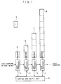
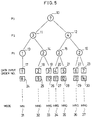
- FIG. 6 A conventional control data generator for a sort processor such as shown in FIG. 1 of the Proceedings of the Japanese Electronic Communications Society, J66-D, March 1983, p 333, is shown in FIG. 6.
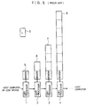
- the control data generator includes four sort processors 1-4, four memories 5-8 each corresponding to each sort processor, and an indicator 9 for the length (L) of data set by the sort processor.
- the i-th sort processor from left is provided with a memory which has a capacity of 2 i-I L.
- the data to be sorted is sequentially input into the sort processor 1.
- the sort processor 1 stores one of the input data in the memory 5 and compares it with the next input data. For sorting in descending order, the sort processor 1 first outputs the greater one between the two data and then the smaller one to the next sort processor 2. This operation is repeated in the sort processor 1.
- the sort processor 2 stores the descending order 2 data set in the memory 6, in which the two data are sorted in descending order, and merges it with the next input descending order 2-data set to output a descending order 4 data set to the sort processor 3. This operation is repeated in the sort processor 2.
- the i-th sort processor merges the descending order 2 i-1 -data set sent from the (i-1)th sort processor to output a descending order 2 i -data set to the (i+1)th sort processor. This operation is repeated in the i-th sort processor.
- the sort processor 3 outputs a descending order 7-data set having a data length of 7 to the sort processor 4 and repeats this operation.
- the sort processor 2 repeats outputting a descending order 3-data set and a descending order 4-data set to the sort processor 3.
- the sort processor 1 repeats outputting descending order 1-data, 2 data, 2-data, and 2-data sets to the sort processor 2.
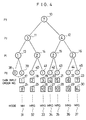
- the data 17-30 to be input to the sort processor are shown in the inputting order.
- Symbols NM 31 and MRG 32-37 indicate that the sort processor 1 is brought into control in the NM mode for data 17 and 24 and into the MRG mode for data 18, 25, etc., respectively.
- the value (n) of a descending order n-data set to be generated by the sort processor 3 is shown at 10.
- the values (n) of descending order n-data sets to he generated by the sort processor 2 are shown at 11 and 12.
- the values (n) of descending order n-data sets to be generated periodically by the sort processor 1 are shown at 13-16.
- the sort processors 1, 2, and 3 in FIG. 6 are represented by P1, P2, and P3.
- the third sort processor 3 always outputs a descending order 7-data set to the fourth sort processor 4.
- the control data generator for a sort processor of FIG. 6 it is possible to sort 14 data under the above conditions.
- the procedure of generating the control data is so complex that there are no ways but by programming. As a result, the sorting capability has been impaired.
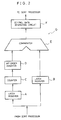
- This control data generator further includes a control data output unit G.
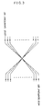
- the control data output unit G includes a pair of latch registers A and B for storing information about the length of data input from a disk device, etc., a counter C for counting the output of the latch register A, a bit order inverter D for converting the most significant bit to the least significant bit of an output from the counter C, the second MSB to the second LSB, and so on as shown in FIG. 3, a comparator E for comparing the output of the bit order inverter D with the output of the latch register B, and a control Data generating unit F for generating control data based on the output of the comparator E.
- the control data is used for switching between the first function or NM mode in which the input data is stored in the corresponding memory outputted without merging and the second function or MRG mode in which the input data are merged in the specific order and outputted from the corresponding memory for later use.
- Each sort processors 1-4 has both the NM mode and the MRG mode.
- the comparator E of FIG. 2 is designed to output a logic 0 when a signal from the bit order inverter D is greater than a signal from the latch register B and otherwise a logic 1.
- control data output unit G starts generating control data.
- control data When the control data is generated, the data is transferred from the latch register A to the counter C for counting.
- the data from the counter C is inverted in bit order by the bit order inverter D and then compared in the comparator E with the data from the latch register B.
- the control data generating circuit F outputs control data indicative of the NM mode if the comparison result is a logic 1 and control data indicative of the MRG mode for the present and next input data if the comparison result is a logic 0.
- the content of the counter C is decreased by 1.
- this content becomes negative, it is transferred from latch register A to the counter C.
- a similar process is repeated for recorded data from a disk device, etc.
- the control data from the control data generating circuit F is transferred to the selected sort processor so that the sort processor operates according to the control data.
- the data input from a disk device, etc. is sorted by the sort processor and transmitted to a host computer, etc.
- an imaginary sort processor P o may be provided to generate the corresponding values 38-45 as shown in FIG. 4.
- the counter C is an increment counter with the initial value of 0.
- the comparator E is modified to output a logic 1 if a value of the data from the bit order inverter D is less than a value of the data from the latch register B and otherwise a logic 0.
- the control data generating circuit F outputs control data about the NM mode if the data of the comparator E is a logic 1 and otherwise control data about the MRG mode.
- the counter C is incremented by 1 when the process of each data is completed and if the comparator E outputs a logic 1, and rest to 0 if the result becomes greater than a value of the latch register A.
- control data output unit G may be connected to only the first sort processor 1 in FIG. 1, and control data may be sequentially transferred from the first sort processor 1 to the second sort processor 2 to the third sort processor 3 along with the input data to thereby simplify the connection between the control data generating unit and the sort processor.
- control data generator for a sort processor includes a control data output unit which consists of a memory for storing information about the input data length and a control data generation circuit for generating control data to make switching between the first and second functions based on the information from the memory, whereby control data is generated efficiently by the simple and inexpensive hardward without using any control data generation program, thus providing the enhanced sorting capability regardless of the data length.
Landscapes
- Engineering & Computer Science (AREA)
- Theoretical Computer Science (AREA)
- General Engineering & Computer Science (AREA)
- Physics & Mathematics (AREA)
- General Physics & Mathematics (AREA)
- Computer Hardware Design (AREA)
- Human Computer Interaction (AREA)
- Information Retrieval, Db Structures And Fs Structures Therefor (AREA)
- Complex Calculations (AREA)
- Management, Administration, Business Operations System, And Electronic Commerce (AREA)
Claims (1)
- Trieur à interclassement en cascade à haute vitesse ayant un mécanisme de syntonisation de format, comprenant- une pluralité de mémoires (5, 6, 7, 8) pour stocker des données d'entrée,- une pluralité de processeurs de triage (1, 2, 3, 4) respectivement connectés auxdites mémoires et ayant une première fonction (NM) pour stocker dans et émettre depuis chaque dite mémoire des données d'entrée, sans interclassement, et deuxième fonction (MRG) pour interclasser les données d'entrée dans un ordre spécifié et émettre lesdites données d'entrée interclassées depuis chaque dite mémoire,- un moyen de production de données de commande (G) connecté auxdits processeurs de triage (1, 2, 3, 4), pour produire des données de commande en fonction d'informations concernant les longueurs desdites données d'entrée et de manière à commuter ledit processeur de triage entre lesdites première et deuxième fonctions,
caractérisé en ce que ledit moyen de production de données de commande (G) comprend :- des premier et deuxième registres de mémorisation (A) et (B) pour stocker lesdites informations concernant les longueurs desdites données d'entrée, de manière que la valeur de nombre entier stockée dans le premier registre de mémorisation (A) soit 2e -1 et la valeur d'un nombre entier stockée dans le deuxième registre de mémorisation (B) soit α₁, obtenu à partir de la valeur d'un nombre entier [2d L/X] = 2e + α, par le dième processeur de triage, et dans lequel L représente la longueur de donnée établie par le trieur à interclassement et X la longueur de données d'entrée fournies depuis l'extérieur et 0 < α < 2e,- un compteur (C) connecté audit premier registre de mémorisation (A) pour compter les données dudit premier registre de mémorisation,- un inverseur d'ordre de bits (D) connecté audit compteur (C) pour convertir au moins le bit de poids le plus fort en le bit de poids le plus faible d'un signal de sortie provenant dudit compteur (C) et- un comparateur (E) connecté audit inverseur d'ordre de bits (D) et audit deuxième registre de mémorisation (B), pour comparer un signal de sortie dudit inverseur d'ordre de bits à un signal de sortie du deuxième registre de mémorisation (B), pour produire une valeur logique afin de placer ledit processeur de triage dans ladite première fonction (NM), lorsque la valeur dudit premier registre de mémorisation (A) est supérieure ou égale à celle dudit deuxième registre de mémorisation (B), et dans ladite deuxième fonction (MRG), lorsque la valeur dudit premier registre de mémorisation (A) est inférieur à celle dudit deuxième registre de mémorisation (B).
Applications Claiming Priority (2)
| Application Number | Priority Date | Filing Date | Title |
|---|---|---|---|
| JP63129023A JP2752634B2 (ja) | 1988-05-26 | 1988-05-26 | ソート処理装置 |
| JP129023/88 | 1988-05-26 |
Publications (3)
| Publication Number | Publication Date |
|---|---|
| EP0343683A2 EP0343683A2 (fr) | 1989-11-29 |
| EP0343683A3 EP0343683A3 (fr) | 1991-10-02 |
| EP0343683B1 true EP0343683B1 (fr) | 1996-04-03 |
Family
ID=14999237
Family Applications (1)
| Application Number | Title | Priority Date | Filing Date |
|---|---|---|---|
| EP89109538A Expired - Lifetime EP0343683B1 (fr) | 1988-05-26 | 1989-05-26 | Générateur de données de commande pour un processeur de triage |
Country Status (5)
| Country | Link |
|---|---|
| US (1) | US5079736A (fr) |
| EP (1) | EP0343683B1 (fr) |
| JP (1) | JP2752634B2 (fr) |
| KR (1) | KR920003176B1 (fr) |
| DE (1) | DE68926131T2 (fr) |
Families Citing this family (12)
| Publication number | Priority date | Publication date | Assignee | Title |
|---|---|---|---|---|
| JPH07104784B2 (ja) * | 1990-04-03 | 1995-11-13 | 富士ゼロックス株式会社 | デジタルデータ処理装置 |
| JPH06242925A (ja) * | 1993-02-15 | 1994-09-02 | Mitsubishi Electric Corp | ソート処理装置 |
| JP3518034B2 (ja) * | 1995-03-30 | 2004-04-12 | 三菱電機株式会社 | ソート方法並びにソート処理装置並びにデータ処理装置 |
| JP3196637B2 (ja) * | 1996-04-26 | 2001-08-06 | 三菱電機株式会社 | ソートプロセッサおよびソート処理装置 |
| US6182071B1 (en) | 1998-05-20 | 2001-01-30 | Mitsubishi Denki Kabushiki Kaisha | Sorting and summing record data including generated sum record with sort level key |
| JP3344559B2 (ja) | 1998-06-19 | 2002-11-11 | 三菱電機株式会社 | マージソート処理装置 |
| DE10052870B4 (de) | 2000-10-20 | 2005-06-23 | Siemens Ag | Vorrichtung zur automatischen Sortierung periodischer Datensätze |
| US7177319B2 (en) * | 2001-12-27 | 2007-02-13 | Interdigital Technology Corporation | Insertion sorter |
| US8190943B2 (en) * | 2009-03-13 | 2012-05-29 | Massachusetts Institute Of Technology | Systolic merge sorter |
| TW201115459A (en) * | 2009-10-21 | 2011-05-01 | Etron Technology Inc | Data processing circuit |
| CN109460210B (zh) * | 2018-10-22 | 2020-11-03 | 重庆中科云从科技有限公司 | 排序系统及数据处理方法 |
| US11249651B2 (en) * | 2019-10-29 | 2022-02-15 | Samsung Electronics Co., Ltd. | System and method for hierarchical sort acceleration near storage |
Family Cites Families (11)
| Publication number | Priority date | Publication date | Assignee | Title |
|---|---|---|---|---|
| US3713107A (en) * | 1972-04-03 | 1973-01-23 | Ncr | Firmware sort processor system |
| US4078260A (en) * | 1976-05-12 | 1978-03-07 | International Business Machines Corporation | Apparatus for transposition sorting of equal length records in overlap relation with record loading and extraction |
| US4209845A (en) * | 1977-01-25 | 1980-06-24 | International Business Machines Corporation | File qualifying and sorting system |
| US4425617A (en) * | 1981-03-23 | 1984-01-10 | Rca Corporation | High-speed data sorter |
| US4514826A (en) * | 1981-05-18 | 1985-04-30 | Tokyo Shibaura Denki Kabushiki Kaisha | Relational algebra engine |
| US4464732A (en) * | 1982-03-19 | 1984-08-07 | Honeywell Inc. | Prioritized sorting system |
| US4575798A (en) * | 1983-06-03 | 1986-03-11 | International Business Machines Corporation | External sorting using key value distribution and range formation |
| JPH0782426B2 (ja) * | 1984-08-22 | 1995-09-06 | 株式会社日立製作所 | マージ・ソート方法および装置 |
| US4799152A (en) * | 1984-10-12 | 1989-01-17 | University Of Pittsburgh | Pipeline feedback array sorter with multi-string sort array and merge tree array |
| US4873625A (en) * | 1987-11-17 | 1989-10-10 | International Business Machines Corporation | Method and apparatus for extending collation functions of a sorting program |
| US4991134A (en) * | 1988-03-30 | 1991-02-05 | International Business Machines Corporation | Concurrent sorting apparatus and method using FIFO stacks |
-
1988
- 1988-05-26 JP JP63129023A patent/JP2752634B2/ja not_active Expired - Lifetime
-
1989
- 1989-05-18 KR KR1019890006637A patent/KR920003176B1/ko not_active Expired
- 1989-05-26 DE DE68926131T patent/DE68926131T2/de not_active Expired - Lifetime
- 1989-05-26 EP EP89109538A patent/EP0343683B1/fr not_active Expired - Lifetime
- 1989-05-26 US US07/357,128 patent/US5079736A/en not_active Expired - Lifetime
Also Published As
| Publication number | Publication date |
|---|---|
| EP0343683A2 (fr) | 1989-11-29 |
| KR900018793A (ko) | 1990-12-22 |
| KR920003176B1 (ko) | 1992-04-23 |
| JPH01297723A (ja) | 1989-11-30 |
| DE68926131T2 (de) | 1996-08-29 |
| JP2752634B2 (ja) | 1998-05-18 |
| DE68926131D1 (de) | 1996-05-09 |
| EP0343683A3 (fr) | 1991-10-02 |
| US5079736A (en) | 1992-01-07 |
Similar Documents
| Publication | Publication Date | Title |
|---|---|---|
| EP0343683B1 (fr) | Générateur de données de commande pour un processeur de triage | |
| US4270181A (en) | Data processing system having a high speed pipeline processing architecture | |
| EP0240032A2 (fr) | Processeur à vecteur avec possibilité de compression/expansion de données vecteur | |
| US5918252A (en) | Apparatus and method for generating a modulo address | |
| US5349684A (en) | Sort and merge system using tags associated with the current records being sorted to lookahead and determine the next record to be sorted | |
| US5471600A (en) | Address generating circuit using a base pointer of loop area | |
| EP0886207B1 (fr) | Détection de coincidence maximale de données utilisant des unitées de mémoire associatives à données entrelacées | |
| US4148017A (en) | Device for detecting a key switch operation | |
| US4907171A (en) | Image size converter | |
| US5319651A (en) | Data integrity features for a sort accelerator | |
| US5142687A (en) | Sort accelerator with rebound sorter repeatedly merging sorted strings | |
| US5185849A (en) | Digital fuzzy inference apparatus having time divisional control function | |
| EP0568374B1 (fr) | Comparateur de magnitude en parallelle pour comparer un nombre binaire à un nombre donné | |
| US5383142A (en) | Fast circuit and method for detecting predetermined bit patterns | |
| US4224680A (en) | Parity prediction circuit for adder/counter | |
| US5129066A (en) | Bit mask generator circuit using multiple logic units for generating a bit mask sequence | |
| US5633816A (en) | Random number generator with wait control circuitry to enhance randomness of numbers read therefrom | |
| Miller et al. | Highly efficient exhaustive search algorithm for optimizing canonical Reed-Muller expansions of boolean functions | |
| US5796918A (en) | Method for ranking membership function values of linguistic input values in a fuzzy logic processor and arrangement for the implementation thereof | |
| US4562763A (en) | Waveform information generating system | |
| US5920493A (en) | Apparatus and method to determine a most significant bit | |
| KR940001150A (ko) | 부분적으로 디코드된 테스트 어드레스 발생기 및 카운트 발생 방법 | |
| US5357235A (en) | Parallelized magnitude comparator | |
| EP0564137A1 (fr) | Soustracteur parallèlisé à retenue anticipée | |
| US5920496A (en) | High speed correlator using up/down counter |
Legal Events
| Date | Code | Title | Description |
|---|---|---|---|
| PUAI | Public reference made under article 153(3) epc to a published international application that has entered the european phase |
Free format text: ORIGINAL CODE: 0009012 |
|
| AK | Designated contracting states |
Kind code of ref document: A2 Designated state(s): DE FR GB |
|
| 17P | Request for examination filed |
Effective date: 19901228 |
|
| PUAL | Search report despatched |
Free format text: ORIGINAL CODE: 0009013 |
|
| AK | Designated contracting states |
Kind code of ref document: A3 Designated state(s): DE FR GB |
|
| 17Q | First examination report despatched |
Effective date: 19940121 |
|
| GRAH | Despatch of communication of intention to grant a patent |
Free format text: ORIGINAL CODE: EPIDOS IGRA |
|
| GRAA | (expected) grant |
Free format text: ORIGINAL CODE: 0009210 |
|
| AK | Designated contracting states |
Kind code of ref document: B1 Designated state(s): DE FR GB |
|
| REF | Corresponds to: |
Ref document number: 68926131 Country of ref document: DE Date of ref document: 19960509 |
|
| ET | Fr: translation filed | ||
| PLBE | No opposition filed within time limit |
Free format text: ORIGINAL CODE: 0009261 |
|
| STAA | Information on the status of an ep patent application or granted ep patent |
Free format text: STATUS: NO OPPOSITION FILED WITHIN TIME LIMIT |
|
| 26N | No opposition filed | ||
| REG | Reference to a national code |
Ref country code: GB Ref legal event code: 746 Effective date: 20000622 |
|
| REG | Reference to a national code |
Ref country code: FR Ref legal event code: D6 |
|
| REG | Reference to a national code |
Ref country code: GB Ref legal event code: IF02 |
|
| PGFP | Annual fee paid to national office [announced via postgrant information from national office to epo] |
Ref country code: DE Payment date: 20080529 Year of fee payment: 20 |
|
| PGFP | Annual fee paid to national office [announced via postgrant information from national office to epo] |
Ref country code: GB Payment date: 20080528 Year of fee payment: 20 |
|
| REG | Reference to a national code |
Ref country code: GB Ref legal event code: PE20 Expiry date: 20090525 |
|
| PG25 | Lapsed in a contracting state [announced via postgrant information from national office to epo] |
Ref country code: GB Free format text: LAPSE BECAUSE OF EXPIRATION OF PROTECTION Effective date: 20090525 |
|
| PGFP | Annual fee paid to national office [announced via postgrant information from national office to epo] |
Ref country code: FR Payment date: 20080514 Year of fee payment: 20 |