EP0342806A1 - Verfahren zur Herstellung von durch Plasma unterstützte chemische Dampfabscheidung auf dielektrischen Schichten gebildeten Strukturen - Google Patents
Verfahren zur Herstellung von durch Plasma unterstützte chemische Dampfabscheidung auf dielektrischen Schichten gebildeten Strukturen Download PDFInfo
- Publication number
- EP0342806A1 EP0342806A1 EP89304189A EP89304189A EP0342806A1 EP 0342806 A1 EP0342806 A1 EP 0342806A1 EP 89304189 A EP89304189 A EP 89304189A EP 89304189 A EP89304189 A EP 89304189A EP 0342806 A1 EP0342806 A1 EP 0342806A1
- Authority
- EP
- European Patent Office
- Prior art keywords
- metal electrode
- substrate
- pecvd
- vapor deposition
- patterned
- Prior art date
- Legal status (The legal status is an assumption and is not a legal conclusion. Google has not performed a legal analysis and makes no representation as to the accuracy of the status listed.)
- Withdrawn
Links
- 238000000034 method Methods 0.000 title claims abstract description 16
- 238000000623 plasma-assisted chemical vapour deposition Methods 0.000 title claims description 25
- 239000000758 substrate Substances 0.000 claims abstract description 34
- 229910052751 metal Inorganic materials 0.000 claims abstract description 29
- 239000002184 metal Substances 0.000 claims abstract description 29
- 238000000151 deposition Methods 0.000 claims abstract description 11
- 239000000376 reactant Substances 0.000 claims abstract description 5
- 238000007740 vapor deposition Methods 0.000 claims 1
- VYPSYNLAJGMNEJ-UHFFFAOYSA-N Silicium dioxide Chemical compound O=[Si]=O VYPSYNLAJGMNEJ-UHFFFAOYSA-N 0.000 description 8
- 230000008021 deposition Effects 0.000 description 7
- 235000012239 silicon dioxide Nutrition 0.000 description 7
- 239000010453 quartz Substances 0.000 description 6
- 238000005530 etching Methods 0.000 description 4
- GQPLMRYTRLFLPF-UHFFFAOYSA-N Nitrous Oxide Chemical compound [O-][N+]#N GQPLMRYTRLFLPF-UHFFFAOYSA-N 0.000 description 3
- 239000007789 gas Substances 0.000 description 3
- 230000000873 masking effect Effects 0.000 description 3
- QGZKDVFQNNGYKY-UHFFFAOYSA-N Ammonia Chemical compound N QGZKDVFQNNGYKY-UHFFFAOYSA-N 0.000 description 2
- KRHYYFGTRYWZRS-UHFFFAOYSA-N Fluorane Chemical compound F KRHYYFGTRYWZRS-UHFFFAOYSA-N 0.000 description 2
- 229910052581 Si3N4 Inorganic materials 0.000 description 2
- 239000000919 ceramic Substances 0.000 description 2
- 239000003989 dielectric material Substances 0.000 description 2
- 239000011810 insulating material Substances 0.000 description 2
- VNWKTOKETHGBQD-UHFFFAOYSA-N methane Chemical compound C VNWKTOKETHGBQD-UHFFFAOYSA-N 0.000 description 2
- 229910052710 silicon Inorganic materials 0.000 description 2
- 239000010703 silicon Substances 0.000 description 2
- HQVNEWCFYHHQES-UHFFFAOYSA-N silicon nitride Chemical compound N12[Si]34N5[Si]62N3[Si]51N64 HQVNEWCFYHHQES-UHFFFAOYSA-N 0.000 description 2
- OKTJSMMVPCPJKN-UHFFFAOYSA-N Carbon Chemical compound [C] OKTJSMMVPCPJKN-UHFFFAOYSA-N 0.000 description 1
- BLRPTPMANUNPDV-UHFFFAOYSA-N Silane Chemical compound [SiH4] BLRPTPMANUNPDV-UHFFFAOYSA-N 0.000 description 1
- XUIMIQQOPSSXEZ-UHFFFAOYSA-N Silicon Chemical compound [Si] XUIMIQQOPSSXEZ-UHFFFAOYSA-N 0.000 description 1
- -1 Silicon Oxy Nitride Chemical class 0.000 description 1
- 229910052782 aluminium Inorganic materials 0.000 description 1
- XAGFODPZIPBFFR-UHFFFAOYSA-N aluminium Chemical compound [Al] XAGFODPZIPBFFR-UHFFFAOYSA-N 0.000 description 1
- 229910021529 ammonia Inorganic materials 0.000 description 1
- QVGXLLKOCUKJST-UHFFFAOYSA-N atomic oxygen Chemical compound [O] QVGXLLKOCUKJST-UHFFFAOYSA-N 0.000 description 1
- 230000015572 biosynthetic process Effects 0.000 description 1
- 229910002804 graphite Inorganic materials 0.000 description 1
- 239000010439 graphite Substances 0.000 description 1
- 238000012986 modification Methods 0.000 description 1
- 230000004048 modification Effects 0.000 description 1
- 239000001272 nitrous oxide Substances 0.000 description 1
- 239000000615 nonconductor Substances 0.000 description 1
- 229910052760 oxygen Inorganic materials 0.000 description 1
- 239000001301 oxygen Substances 0.000 description 1
- 229920002120 photoresistant polymer Polymers 0.000 description 1
- 238000007789 sealing Methods 0.000 description 1
- 239000004065 semiconductor Substances 0.000 description 1
- 229910000077 silane Inorganic materials 0.000 description 1
- HBMJWWWQQXIZIP-UHFFFAOYSA-N silicon carbide Chemical compound [Si+]#[C-] HBMJWWWQQXIZIP-UHFFFAOYSA-N 0.000 description 1
- 229910010271 silicon carbide Inorganic materials 0.000 description 1
- 239000000377 silicon dioxide Substances 0.000 description 1
Images


Classifications
-
- C—CHEMISTRY; METALLURGY
- C23—COATING METALLIC MATERIAL; COATING MATERIAL WITH METALLIC MATERIAL; CHEMICAL SURFACE TREATMENT; DIFFUSION TREATMENT OF METALLIC MATERIAL; COATING BY VACUUM EVAPORATION, BY SPUTTERING, BY ION IMPLANTATION OR BY CHEMICAL VAPOUR DEPOSITION, IN GENERAL; INHIBITING CORROSION OF METALLIC MATERIAL OR INCRUSTATION IN GENERAL
- C23C—COATING METALLIC MATERIAL; COATING MATERIAL WITH METALLIC MATERIAL; SURFACE TREATMENT OF METALLIC MATERIAL BY DIFFUSION INTO THE SURFACE, BY CHEMICAL CONVERSION OR SUBSTITUTION; COATING BY VACUUM EVAPORATION, BY SPUTTERING, BY ION IMPLANTATION OR BY CHEMICAL VAPOUR DEPOSITION, IN GENERAL
- C23C16/00—Chemical coating by decomposition of gaseous compounds, without leaving reaction products of surface material in the coating, i.e. chemical vapour deposition [CVD] processes
- C23C16/04—Coating on selected surface areas, e.g. using masks
- C23C16/047—Coating on selected surface areas, e.g. using masks using irradiation by energy or particles
-
- C—CHEMISTRY; METALLURGY
- C23—COATING METALLIC MATERIAL; COATING MATERIAL WITH METALLIC MATERIAL; CHEMICAL SURFACE TREATMENT; DIFFUSION TREATMENT OF METALLIC MATERIAL; COATING BY VACUUM EVAPORATION, BY SPUTTERING, BY ION IMPLANTATION OR BY CHEMICAL VAPOUR DEPOSITION, IN GENERAL; INHIBITING CORROSION OF METALLIC MATERIAL OR INCRUSTATION IN GENERAL
- C23C—COATING METALLIC MATERIAL; COATING MATERIAL WITH METALLIC MATERIAL; SURFACE TREATMENT OF METALLIC MATERIAL BY DIFFUSION INTO THE SURFACE, BY CHEMICAL CONVERSION OR SUBSTITUTION; COATING BY VACUUM EVAPORATION, BY SPUTTERING, BY ION IMPLANTATION OR BY CHEMICAL VAPOUR DEPOSITION, IN GENERAL
- C23C16/00—Chemical coating by decomposition of gaseous compounds, without leaving reaction products of surface material in the coating, i.e. chemical vapour deposition [CVD] processes
- C23C16/44—Chemical coating by decomposition of gaseous compounds, without leaving reaction products of surface material in the coating, i.e. chemical vapour deposition [CVD] processes characterised by the method of coating
- C23C16/50—Chemical coating by decomposition of gaseous compounds, without leaving reaction products of surface material in the coating, i.e. chemical vapour deposition [CVD] processes characterised by the method of coating using electric discharges
- C23C16/505—Chemical coating by decomposition of gaseous compounds, without leaving reaction products of surface material in the coating, i.e. chemical vapour deposition [CVD] processes characterised by the method of coating using electric discharges using radio frequency discharges
- C23C16/509—Chemical coating by decomposition of gaseous compounds, without leaving reaction products of surface material in the coating, i.e. chemical vapour deposition [CVD] processes characterised by the method of coating using electric discharges using radio frequency discharges using internal electrodes
Definitions
- This invention relates generally to the plasma enhanced chemical vapor deposition (PECVD) of insulating materials on selected substrates and more particularly to such processes for forming thin patterned dielectric layers which are PECVD deposited on the substrates.
- PECVD plasma enhanced chemical vapor deposition
- a PECVD reactor for depositing dielectric materials such as silicon dioxide, silicon nitride, silicon carbide, and the like, and such a reactor will typically include a quartz tube which is maintained at a pressure of about 1 Torr or greater.
- the reactive gasses such as silane, oxygen, nitrous oxide, ammonia and methane which are frequently used in this process are introduced into the quartz tube which is typically maintained at a temperature in the range of between 200 o C and 400 o C.
- the substrates that are to be deposited with a dielectric material are placed on electrodes which are typically made of graphite or aluminum, and R.F. power is applied to these electrodes to thereby create an R.F. plasma between the electrodes. This plasma dissociates and excites the reactive species within the reactor, and these reactive species in turn react with each other and thereby deposit a continuous layer of an insulating material on the substrate.
- etching process In order to then form a desired pattern in the thus deposited dielectric layer, it becomes necessary to employ some type of selective etching process to remove certain regions of the dielectric layer, as is well known.
- conventional photolithographic masking, ultraviolet exposure and etching processes may be first used to form a photoresist mask on the dielectric layer, and then a selective etchant such as dilute hydrofluoric acid or a reactive plasma may then be used to remove the unprotected areas of the photoresist-masked dielectric layer to thereby form a desired pattern of openings therein.
- the general purpose of the present invention is to eliminate the need for the above described masking and selective etching process in order to provide and form the desired pattern of openings in the plasma deposited dielectric layer, thereby greatly reducing the cost and complexity of the dielectric pattern forming process.
- a novel plasma enhanced chemical vapor deposition process for forming these dielectric patterns on selected substrates. This process includes initially providing a patterned metal electrode adjacent to one surface of a chosen substrate. Selected reactive gasses are provided in the vicinity of the patterned metal electrode and under conditions of predetermined elevated temperature and controlled pressure.
- RF power is applied to the patterned metal electrode so as to dissociate and excite certain reactive species within these gasses and cause the species to react with one another and thereby selectively deposit only on the area of the chosen substrate which is coextensive with the adjacent metal in the patterned metal electrode.
- a plasma enhanced chemical vapor deposition (PECVD) reactor including a quartz tube 10 which is connected by way of exhaust tube 12 to a vacuum pump (not shown).
- the quartz tube 10 is integrally joined to a vertical end wall 14, and the end wall 14 is in turn adapted to receive a cover plate 16 for sealing off the tube 10 during a PECVD operation.
- Resistive heater elements 18 are positioned as shown adjacent to the tube 10 in order to heat the tube to a desired elevated temperature.
- RF power is made available inside the tube 10 as indicated by way of electrodes 20 and 22 which extend as shown through the end cover plate 16 and through the end wall 14.
- These RF electrodes 20 and 22 are electrically connected to spring biased end connectors 24 and 26 which extend into the quartz tube 10 and on opposite sides of the path 28 of reactant gas flow emanating from the gas input tube 30.
- the patterned electrodes 36 and 38 can be rolled in and out of the reactor tube 10 on the rollers 34 affixed to the same.
- Each of the metal electrodes 36 and 38 include, for example only, a plurality of openings 40 and 42 (shown in the figure as rectangular, but may be any desired geometrical shape).
- the openings 40 and 42 correspond to the desired openings in a dielectric pattern to be formed in the manner described below.
- These rectangular openings 40 and 42 are covered by a substrate 44 (indicated by the dotted line) upon which it is desired to form a patterned dielectric layer with openings therein corresponding to and coextensive with the openings 40 and 42 in the metal electrode 36.
- FIG. 2 there is shown one suitable clip-on arrangement which may be used for securing the substrates 44 to the metal electrodes 36.
- a pair of spring loaded clips 43 and 45 are secured to the back side of an electrode 36 and will hold a substrate 44 temporarily in place during a PECVD operation.
- FIG. 3B the cross section view in Figure 3B is taken along lines B-B of Figure 3A after the PECVD deposition has taken place and shows three focused deposition areas within which a dielectric pattern indicated as 46,48 and 50 is deposited on the left hand substrate 52. These areas correspond to sections of the metal regions 54,56 and 58 in the left hand metal electrode which are coextensive with the substrate 52. Similarly, a dielectric pattern defined by regions 60,62 and 64 is deposited on the right hand substrate 66 which is positioned as shown on the right hand metal electrode, including metal regions 68,70 and 72 therein.
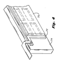
- the metal electrode pattern 72 in Figure 4 is affixed to an underlying support member 74, such as a ceramic substrate.
- the substrate 74 has the property of being an excellent electrical insulator and is capable of withstanding elevated temperatures in the plasma enhanced PECVD reactor.
- the elongated deposition substrates 76 and 78 shown in Figure 5A cover the entire series of openings in the underlying metal electrodes 72.
- the PECVD deposition operation is the same as the deposition operation described above with reference Figures 3A and 3B and provides for the dielectric plasma enhanced chemical vapor deposition of a pattern 82,84 and 86 on the left hand substrate 76 and the pattern 90,92 and 94 on the right hand substrate 78 as indicated in Figure 5B.
- the substrates to be deposited may be mounted on a support member having no electrodes thereon and then patterned on one surface thereon using a removable electrode pattern temporarily laid over the support member surface and connected to source of RF power.
- the patterned insulating layers may be formed in any desired geometry in accordance with the chosen geometries of the metal electrode patterns.
- the following example provides certain reactant gasses, gas flow rates, temperature and pressure which will be suitable for the deposition of one particular type of dielectric pattern on a silicon substrate: Dielectric Film Reactant Gasses Temperature Pressure Silicon Nitride Silane-250 standard cubic centimeters per minute (sccm) 350°C 0.7 Torr Amnionia-2000 sccm Silicon Oxy Nitride Silane-250 sccm 350°C 1.0 Torr Nitrous Oxide-2000 sccm
Landscapes
- Chemical & Material Sciences (AREA)
- Engineering & Computer Science (AREA)
- Materials Engineering (AREA)
- General Chemical & Material Sciences (AREA)
- Chemical Kinetics & Catalysis (AREA)
- Mechanical Engineering (AREA)
- Metallurgy (AREA)
- Organic Chemistry (AREA)
- Physics & Mathematics (AREA)
- Plasma & Fusion (AREA)
- Toxicology (AREA)
- Health & Medical Sciences (AREA)
- Chemical Vapour Deposition (AREA)
Applications Claiming Priority (2)
| Application Number | Priority Date | Filing Date | Title |
|---|---|---|---|
| US195236 | 1980-10-20 | ||
| US07/195,236 US4844945A (en) | 1988-05-18 | 1988-05-18 | Process for producing patterns in dielectric layers formed by plasma enhanced chemical vapor deposition (PECVD) |
Publications (1)
| Publication Number | Publication Date |
|---|---|
| EP0342806A1 true EP0342806A1 (de) | 1989-11-23 |
Family
ID=22720589
Family Applications (1)
| Application Number | Title | Priority Date | Filing Date |
|---|---|---|---|
| EP89304189A Withdrawn EP0342806A1 (de) | 1988-05-18 | 1989-04-26 | Verfahren zur Herstellung von durch Plasma unterstützte chemische Dampfabscheidung auf dielektrischen Schichten gebildeten Strukturen |
Country Status (4)
| Country | Link |
|---|---|
| US (1) | US4844945A (de) |
| EP (1) | EP0342806A1 (de) |
| JP (1) | JPH0231423A (de) |
| CA (1) | CA1333786C (de) |
Cited By (1)
| Publication number | Priority date | Publication date | Assignee | Title |
|---|---|---|---|---|
| TWI411701B (zh) * | 2011-04-22 | 2013-10-11 | Archers Inc | 電漿輔助式化學氣相沉積裝置 |
Families Citing this family (6)
| Publication number | Priority date | Publication date | Assignee | Title |
|---|---|---|---|---|
| US5064681A (en) * | 1986-08-21 | 1991-11-12 | International Business Machines Corporation | Selective deposition process for physical vapor deposition |
| US5275665A (en) * | 1988-06-06 | 1994-01-04 | Research Development Corporation Of Japan | Method and apparatus for causing plasma reaction under atmospheric pressure |
| US6194038B1 (en) * | 1998-03-20 | 2001-02-27 | Applied Materials, Inc. | Method for deposition of a conformal layer on a substrate |
| FI20080248A7 (fi) * | 2008-03-28 | 2009-09-29 | Savcor Face Group Oy | Kemiallinen kaasufaasipinnoite ja menetelmä kaasufaasipinnoitteen muodostamiseksi |
| US9018108B2 (en) | 2013-01-25 | 2015-04-28 | Applied Materials, Inc. | Low shrinkage dielectric films |
| CN103911599B (zh) * | 2014-03-26 | 2016-02-10 | 京东方科技集团股份有限公司 | 一种等离子体增强化学气相沉积装置 |
Citations (3)
| Publication number | Priority date | Publication date | Assignee | Title |
|---|---|---|---|---|
| EP0199585A2 (de) * | 1985-04-23 | 1986-10-29 | Seiko Instruments Inc. | Vorrichtung zur Abscheidung eines elektrisch leitenden und/oder nichtleitenden Materials auf einem Gegenstand |
| EP0240305A2 (de) * | 1986-03-31 | 1987-10-07 | Canon Kabushiki Kaisha | Herstellungsverfahren einer niedergeschlagenen Schicht |
| GB2194556A (en) * | 1986-08-21 | 1988-03-09 | Special Research Systems Limit | Plasma enhanced chemical vapour deposition of films |
Family Cites Families (1)
| Publication number | Priority date | Publication date | Assignee | Title |
|---|---|---|---|---|
| US4550257A (en) * | 1984-06-29 | 1985-10-29 | International Business Machines Corporation | Narrow line width pattern fabrication |
-
1988
- 1988-05-18 US US07/195,236 patent/US4844945A/en not_active Expired - Lifetime
-
1989
- 1989-01-25 CA CA000589157A patent/CA1333786C/en not_active Expired - Fee Related
- 1989-04-26 EP EP89304189A patent/EP0342806A1/de not_active Withdrawn
- 1989-05-18 JP JP1125471A patent/JPH0231423A/ja active Pending
Patent Citations (3)
| Publication number | Priority date | Publication date | Assignee | Title |
|---|---|---|---|---|
| EP0199585A2 (de) * | 1985-04-23 | 1986-10-29 | Seiko Instruments Inc. | Vorrichtung zur Abscheidung eines elektrisch leitenden und/oder nichtleitenden Materials auf einem Gegenstand |
| EP0240305A2 (de) * | 1986-03-31 | 1987-10-07 | Canon Kabushiki Kaisha | Herstellungsverfahren einer niedergeschlagenen Schicht |
| GB2194556A (en) * | 1986-08-21 | 1988-03-09 | Special Research Systems Limit | Plasma enhanced chemical vapour deposition of films |
Cited By (1)
| Publication number | Priority date | Publication date | Assignee | Title |
|---|---|---|---|---|
| TWI411701B (zh) * | 2011-04-22 | 2013-10-11 | Archers Inc | 電漿輔助式化學氣相沉積裝置 |
Also Published As
| Publication number | Publication date |
|---|---|
| CA1333786C (en) | 1995-01-03 |
| JPH0231423A (ja) | 1990-02-01 |
| US4844945A (en) | 1989-07-04 |
Similar Documents
| Publication | Publication Date | Title |
|---|---|---|
| US5017264A (en) | Method of eliminating carbon material by chemical vapor reaction | |
| US6165916A (en) | Film-forming method and film-forming apparatus | |
| US5084130A (en) | Method for depositing material on depressions | |
| US5015330A (en) | Film forming method and film forming device | |
| JP4335438B2 (ja) | 非対称の流動形状を用いるプロセスチャンバ用リッドアセンブリ | |
| US4624214A (en) | Dry-processing apparatus | |
| US4693779A (en) | Manufacturing apparatus for semiconductor devices | |
| KR920010728B1 (ko) | 반도체 제조장치 | |
| JP2004165682A (ja) | 薄膜トランジスタのための多段階cvd法 | |
| JPH08279498A (ja) | ラインプラズマ気相堆積装置及び方法 | |
| US5176789A (en) | Method for depositing material on depressions | |
| EP0342806A1 (de) | Verfahren zur Herstellung von durch Plasma unterstützte chemische Dampfabscheidung auf dielektrischen Schichten gebildeten Strukturen | |
| JPH02234419A (ja) | プラズマ電極 | |
| JPH05217922A (ja) | プラズマによる気相からの層析出方法 | |
| US5281557A (en) | Soluble oxides for integrated circuit fabrication formed by the incomplete dissociation of the precursor gas | |
| US4836902A (en) | Method and apparatus for removing coating from substrate | |
| JPH07272897A (ja) | マイクロ波プラズマ装置 | |
| JPH0610140A (ja) | 薄膜堆積装置 | |
| JP2630089B2 (ja) | マイクロ波プラズマ処理装置 | |
| EP1154038A1 (de) | Verfahren zum Konditionieren von einem CVD Reaktionskammer | |
| JPH01189114A (ja) | 気相成長装置 | |
| JPH04154117A (ja) | 減圧cvd装置 | |
| JPH0633245A (ja) | Cvd装置 | |
| JP3522738B2 (ja) | 化学気相成長による金属薄膜形成方法 | |
| JPS58171563A (ja) | チユ−ブ型プラズマcvd装置 |
Legal Events
| Date | Code | Title | Description |
|---|---|---|---|
| PUAI | Public reference made under article 153(3) epc to a published international application that has entered the european phase |
Free format text: ORIGINAL CODE: 0009012 |
|
| AK | Designated contracting states |
Kind code of ref document: A1 Designated state(s): DE FR GB IT |
|
| 17P | Request for examination filed |
Effective date: 19900502 |
|
| 17Q | First examination report despatched |
Effective date: 19911210 |
|
| STAA | Information on the status of an ep patent application or granted ep patent |
Free format text: STATUS: THE APPLICATION IS DEEMED TO BE WITHDRAWN |
|
| 18D | Application deemed to be withdrawn |
Effective date: 19920422 |