EP0342290A2 - Modulationsvorrichtung für optische Strahlen - Google Patents
Modulationsvorrichtung für optische Strahlen Download PDFInfo
- Publication number
- EP0342290A2 EP0342290A2 EP88311005A EP88311005A EP0342290A2 EP 0342290 A2 EP0342290 A2 EP 0342290A2 EP 88311005 A EP88311005 A EP 88311005A EP 88311005 A EP88311005 A EP 88311005A EP 0342290 A2 EP0342290 A2 EP 0342290A2
- Authority
- EP
- European Patent Office
- Prior art keywords
- electrodes
- beams
- modulator
- acoustic
- gauss
- Prior art date
- Legal status (The legal status is an assumption and is not a legal conclusion. Google has not performed a legal analysis and makes no representation as to the accuracy of the status listed.)
- Withdrawn
Links
Images


Classifications
-
- G—PHYSICS
- G02—OPTICS
- G02F—OPTICAL DEVICES OR ARRANGEMENTS FOR THE CONTROL OF LIGHT BY MODIFICATION OF THE OPTICAL PROPERTIES OF THE MEDIA OF THE ELEMENTS INVOLVED THEREIN; NON-LINEAR OPTICS; FREQUENCY-CHANGING OF LIGHT; OPTICAL LOGIC ELEMENTS; OPTICAL ANALOGUE/DIGITAL CONVERTERS
- G02F1/00—Devices or arrangements for the control of the intensity, colour, phase, polarisation or direction of light arriving from an independent light source, e.g. switching, gating or modulating; Non-linear optics
- G02F1/01—Devices or arrangements for the control of the intensity, colour, phase, polarisation or direction of light arriving from an independent light source, e.g. switching, gating or modulating; Non-linear optics for the control of the intensity, phase, polarisation or colour
- G02F1/11—Devices or arrangements for the control of the intensity, colour, phase, polarisation or direction of light arriving from an independent light source, e.g. switching, gating or modulating; Non-linear optics for the control of the intensity, phase, polarisation or colour based on acousto-optical elements, e.g. using variable diffraction by sound or like mechanical waves
Definitions
- the present invention relates to an optical beam modulating device which is necessary in cases where, for example, halftone plate duplicate images are recorded on a recording material by controlling a light-exposure means in accordance with image signals obtained by the photoelectric of an original image, and especially in cases where halftone plate images are recorded by independently modulating a multiple number of Gauss beams (hereinafter, "Gauss beam” means a beam with an energy level which can cause exposure, the peripheral portion of the beam circle where the energy level is too low to be effective in exposure being excluded) on the basis of image signals.
- Gaus beam means a beam with an energy level which can cause exposure, the peripheral portion of the beam circle where the energy level is too low to be effective in exposure being excluded
- the recording of halftone plate images by the relative scanning of a multiple number of light beams (lined up in a row) across the surface of a recording material, with the light beams being independently modulated on the basis of image signals, has conventionally been performed in the art.
- the multiple number of light beams are obtained by installing a multiple number of totally reflective mirrors and semi-reflective mirrors, and splitting a single light beam generated by an argon laser by reflecting the light beam from the mirrors, or by splitting a single light beam using an optical beam splitter of the type described in Japanese Patent Application Laid-Open (Kokai) No. 52-122135.
- the respective light beams thus obtained are independently modulated by means of a multi-channel ultrasonic modulator and then reduced in diameter by means of a crystal optical system and directed onto the surface of a recording material.
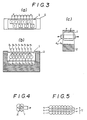
- Figures 3(a), 3(b) and 3(c) illustrate a conventional multi-channel ultrasonic modulator.
- numeral 1 indicates a modulator crystal
- 2 indicate a crystal holder
- 3a through 3h indicate acoustic electrodes. These electrodes are positioned on a side surface of the modulator crystal 1 which runs perpendicular to Gauss beams 4a through 4h, and are installed in two rows with a one-half pitch phase difference between the two rows.
- the pitch p of adjacent Gauss beams in a case where the beam diameters of four gauss beams are caused to overlap in a square arrangement so that the respective beam circles pass through a central point X as shown in Figure 4 is equal to the square root of the square of the beam radius r2 x 2 from the Pythagorean theorem. This is considered to be approximately 0.707 times the beam diameter D of the Gauss beams. If the pitch p is smaller than this value, the point X will not be exposed to the light of the light beams. However, if the pitch of the Gauss beams 4a through 4h is set at p, then the pitch of the acoustic electrodes 3a through 3h is also accurately set at p.
- the acoustic electrodes 3a through 3h generate ultrasonic waves in accordance with desired image signals for the purpose of forming images of various sizes as aggregations of dots on the recording surface. These electrodes independently modulate the Gauss beams 4a through 4h which are directed so that they traverse the respective acoustic electrodes.
- Figure 5 shows one example of the conditions of an aggregation of dots recorded on the recording surface by exposure.
- the recerding material moves continuously in the direction indicated by arrow Y.
- the eight dots in row a are exposed first.
- the eight dots in row b are exposed.
- the eight dots in row c are exposed, completing the aggregation of dots illustrated in Figure 5.
- the generation of ultrasonic waves by the acoustic electrodes 3a through 3h is interrupted when rows a, b and c are exposed.
- the direct passage of the Gauss beams 4a through 4h through the modulator crystal 1 is allowed, so that exposure takes place.
- the direct passage of the Gauss beams 4a through 4h is blocked. In this way, the light beams are ultrasonically modulated.
- the Gauss beams 4a through 4h which pass through the ultrasonic modulator 1 overlap each other. Accordingly, when a light beam corresponding to a given acoustic electrode among the acoustic electrodes 3a through 3h is modulated by the acoustic electrode, the generation of crosstalk interference which cuts the passage of the beam in the adjacent light beams on both sides is essentially unavoidable.
- the abovementioned crosstalk occurs even more conspicuously. Accordingly, the formation of the acoustic electrodes 3a through 3h and the structure and arrangement of the beam splitter which determine the pitch of the Gauss beams must be maintained at a high degree of precision.
- the number of light beams has been limited to approximately 20 due to heat loading of the modulator crystal. For this reason, a long exposure time has been required.
- One object of the present invention is to provide an eptical beam modulating device which makes it possible to modulate the respective light beams independently without generating any crosstalk.
- Another object of the present invention is to provide an optical beam modulating device which can independently modulate the respective light beams with the Gauss beams separated so that they do not overlap, but which is nevertheless capable of modulation so that the Gauss beams may overlap in the form of a connected chain on the recording surface.
- Still another object of the present invention is to provide an optical beam modulating device which is capable of modulation so that the Gauss beams overlap in the form of a connected chain on the recording surface even without a precise match between the size and pitch of the acoustic electrodes and the beam diameter and pitch of the light beams.
- Yet another object of the present invention is to provide an optical beam modulating device in which the number of acoustic electrodes can be greatly increased, so that image resolution can be improved and exposure time shortened.
- a unique structure including two multi-channel optical beam modulators installed side by side, each including modulator crystals of rectangular parallelepiped shape, and having a prescribed number of acoustic electrodes installed on one side surface of each of the modulators.
- the acoustic electrodes are installed at equal pitch intervals so that Gauss beams can be directed across the electrodes separately from each other, and the positions at which the acoustic electrodes of one modulator are installed are shifted by one-half pitch with respect to the positions at which the acoustic electrodes of the other modulator are installed.
- the acoustic electrodes are constructed so that they independently modulate the Gauss beams which traverse the respective acoustic electrodes on the basis of desired image signals, and the acoustic electrodes of the modulator positioned on the downstream side with respect to a recording surface which is scanned by relative motion are constructed so that they modulate with a delay and thus correct the phase discrepancy of the output beams at the recording surface corresponding to the spacing between the two sets of Gauss beams passing through the two modulators.
- Two multi-channel optical beam modulators A and B are installed adjacent to each other, that is, one on top of the other in a holder C, as seen in Figure 1.
- Four acoustic electrodes 7a through 7d are installed at equal intervals, pitch P, on the top surface of the modulator A.
- another four acoustic electrodes 8a through 8d are installed at equal intervals, pitch P, on the bottom surface of the modulator B.
- the upper acoustic electrodes 7a through 7d are shifted by one-half pitch with respect to the lower acoustic electrodes 8a through 8d.
- the pitch P at which the acoustic electrodes of the respective modulators are installed (the pitch P being equal to the pitch P of the Gauss beams 9a through 9d and the pitch P of the Gauss beams 10a through 10d) is set at approximately 1.414 times the beam diameter D of the Gauss beams, then scanning exposure can be accomplished so that four beam circles pass through a central point X as shown in Figure 4.
- the Gauss beams 9a through 9d are separated from the Gauss beams 10a through 10d by the distance H. It is desirable to set the distance H at approximately 0.707 times the beam diameter D of the Gauss beams times an appropriate natural number, so that the output of delay signals to the lower acoustic electrodes 8a through 8d is performed at the same time as the signal output to the upper acoustic electrodes 7a through 7d.
- H it is sufficient to set H at approximately 0.707 times the beam diameter D of the Gauss beams times 5, so that the output delay signals to the lower acoustic electrodes 8a through 8d is delayed by a timing of five rows with respect to the output of signals to the acoustic electrodes 7a through 7d. Since the acoustic electrodes 7a through 7d and the acoustic electrodes 8a through 8d are spaced, crosstalk does not occur. Accordingly, these electrodes may be made larger in size than the beam diameter D of the Gauss beams 9a through 9d and 10a through 10d.
- the electrodes may be larger than the beam diameter, the pitch at which the electrodes are installed does not require a high degree of precision.
- the pitch of the Gauss beams 9a through 9d and 10a through 10d it is necessary to cause the split light beams to be incident so that the pitch is very precise. This can be accomplished, for example, by using two optical beam splitters of the type described in Japanese Patent Application Laid-Open (Kokai) No, 52-122135.
- Figures 2(a) through 2(n) constitute a dot generation process diagram which illustrates the relationship between scanning and modulation in the optical beam modulating device of the present invention.
- Figure 2(a) illustrates a state in which 8 dots x 8 dots have been recorded on a recording surface 11 which moves continuously in the direction indicated by arrow Z. This state is obtained by the process illustrated in Figures 2(c) through 2(n).
- Figure 2(b) illustrates the arrangement of 8 dots obtained when the acoustic electrodes 7a through 7d and 8a through 8d are simultaneously modulated without any delay modulation of the acoustic electrodes 8a through 8d.
- Line BL in Figure 1(a) and line BL in Figures 2(b) through 2(n) indicate the corresponding position in scanning.
- the four dots in row (a) are produced by the Gauss beams 9a through 9d, while the four dots in row (b) are produced by the Gauss beams 10a through 10d.
- the Gauss beams 9a through 9d and 10a through 10d do not overlap; accordingly, no crosstalk can occur.
- the spacing r between row (a) and row (b) in Figure 2(b) corresponds to the spacing H between the Gauss beams 9a through 9d and the Gauss beams 10a through 10d shown in Figure 1(a).
- row (b) is subjected to delay processing so that the spacing r is eliminated.
- Figure 2(c) illustrates a state in which (i) the four dots in row (a1) have first been exposed by the Gauss beams 9a through 9d, after that (ii) the for dots in row (a2) have been exposed by the same Gauss beams after the recording material 11 has moved a distance of p/2 in the direction indicated by arrow Z.
- Figures 2(d) through 2(f) illustrate respective states in which the four dots in rows (a3), (a4) and (a5) have been exposed by the Gauss beams 9a through 9d after the recording material 11 has moved a distance of p/2 in the direction indicated by arrow Z each time.
- Figure 2(g) illustrates a state in which (i) the four dots in row (a6), which is separated by a distance of r from the row (a1), have been exposed by the Gauss beams 9a through 9d, and (ii) the four dots in the first row (b1) have been exposed by the Gauss beams 10a through 10d (which have been modulated with a delay), so that the dots in row (b1) overlap in the form of a connected chain with the four dots in row (a1).
- Figures 2(h) and 2(i), respectively, indicate states in which row (a7) and row (b2), and row (a8) and row (b3), have been exposed by the Gauss beams 9a through 9d and 10a through l0d.
- Figures 2(j) through 2(n) indicate states in which rows (b4), (b5), (b6), (b7) and (b8) have been exposed by the delay-modulated Gauss beams 10a through 10d; these rows overlap in the form of a connected chain with rows (a4), (a5), (a6), (a7) and (a8), respectively.
- the optical beam modulating device of the present invention possesses the following merits:
Landscapes
- Physics & Mathematics (AREA)
- Nonlinear Science (AREA)
- General Physics & Mathematics (AREA)
- Optics & Photonics (AREA)
- Facsimile Scanning Arrangements (AREA)
- Laser Beam Printer (AREA)
- Fax Reproducing Arrangements (AREA)
- Exposure Or Original Feeding In Electrophotography (AREA)
Applications Claiming Priority (2)
| Application Number | Priority Date | Filing Date | Title |
|---|---|---|---|
| JP123605/88 | 1988-05-20 | ||
| JP63123605A JPH01293315A (ja) | 1988-05-20 | 1988-05-20 | 光ビーム変調装置 |
Publications (2)
| Publication Number | Publication Date |
|---|---|
| EP0342290A2 true EP0342290A2 (de) | 1989-11-23 |
| EP0342290A3 EP0342290A3 (de) | 1990-12-19 |
Family
ID=14864747
Family Applications (1)
| Application Number | Title | Priority Date | Filing Date |
|---|---|---|---|
| EP19880311005 Withdrawn EP0342290A3 (de) | 1988-05-20 | 1988-11-21 | Modulationsvorrichtung für optische Strahlen |
Country Status (3)
| Country | Link |
|---|---|
| US (1) | US5122897A (de) |
| EP (1) | EP0342290A3 (de) |
| JP (1) | JPH01293315A (de) |
Cited By (2)
| Publication number | Priority date | Publication date | Assignee | Title |
|---|---|---|---|---|
| WO1999003016A1 (en) * | 1997-07-08 | 1999-01-21 | Etec Systems, Inc. | Acousto-optic modulator array with reduced rf crosstalk |
| KR100446602B1 (ko) * | 1997-11-07 | 2004-11-03 | 삼성전자주식회사 | 다채널음향광변조장치 |
Families Citing this family (1)
| Publication number | Priority date | Publication date | Assignee | Title |
|---|---|---|---|---|
| EP2024783A1 (de) * | 2006-05-30 | 2009-02-18 | BAE Systems PLC | Akustooptische anordnungen |
Family Cites Families (11)
| Publication number | Priority date | Publication date | Assignee | Title |
|---|---|---|---|---|
| US3512871A (en) * | 1965-06-22 | 1970-05-19 | Ibm | Light beam deflection using fourier optics |
| FR2088797A5 (de) * | 1970-04-24 | 1972-01-07 | Thomson Csf | |
| JPS5563269A (en) * | 1978-11-07 | 1980-05-13 | Matsushita Electric Ind Co Ltd | Recording head |
| US4295145A (en) * | 1978-12-29 | 1981-10-13 | International Business Machines Corporation | Acousto-optically modulated laser scanning arrangement for correcting for interference appearing therein |
| US4449212A (en) * | 1981-07-30 | 1984-05-15 | Rca Corporation | Multi-beam optical record and playback apparatus |
| JPS5895321A (ja) * | 1981-12-01 | 1983-06-06 | Ricoh Co Ltd | 光スイツチングアレイ |
| US4541712A (en) * | 1981-12-21 | 1985-09-17 | Tre Semiconductor Equipment Corporation | Laser pattern generating system |
| JPS58117521A (ja) * | 1981-12-30 | 1983-07-13 | Ricoh Co Ltd | Plzt光スイツチングアレイ |
| EP0100238B1 (de) * | 1982-07-27 | 1991-06-26 | Hoya Corporation | Akustooptisches Modulationselement und Vorrichtung mit einem solchen Element |
| US4692016A (en) * | 1986-03-14 | 1987-09-08 | Fondation Suisse Pour La Recherche En Microtechnique | Process for electrophotographic matrix printing and device for carrying out the process |
| JPH01287622A (ja) * | 1988-05-16 | 1989-11-20 | Think Lab Kk | 光ビーム分割器 |
-
1988
- 1988-05-20 JP JP63123605A patent/JPH01293315A/ja active Pending
- 1988-11-21 EP EP19880311005 patent/EP0342290A3/de not_active Withdrawn
- 1988-12-16 US US07/286,633 patent/US5122897A/en not_active Expired - Fee Related
Cited By (2)
| Publication number | Priority date | Publication date | Assignee | Title |
|---|---|---|---|---|
| WO1999003016A1 (en) * | 1997-07-08 | 1999-01-21 | Etec Systems, Inc. | Acousto-optic modulator array with reduced rf crosstalk |
| KR100446602B1 (ko) * | 1997-11-07 | 2004-11-03 | 삼성전자주식회사 | 다채널음향광변조장치 |
Also Published As
| Publication number | Publication date |
|---|---|
| JPH01293315A (ja) | 1989-11-27 |
| EP0342290A3 (de) | 1990-12-19 |
| US5122897A (en) | 1992-06-16 |
Similar Documents
| Publication | Publication Date | Title |
|---|---|---|
| US4686542A (en) | High speed, high resolution raster output scanner | |
| EP0299964B1 (de) | Abtastvorrichtung | |
| US4950888A (en) | Scanning beam synchronization system | |
| US4960320A (en) | Optical beam splitting method and an optical beam splitting/modulation method | |
| EP0288970B1 (de) | Optisches System für ein Lichtpunktabtastsystem | |
| US5122897A (en) | Optical beam modulating device | |
| US4502757A (en) | Light beam distributor and an acousto-optic light modulating element | |
| US5258856A (en) | Scanning and exposing method using a plurality of optical beams and apparatus therefor | |
| US5309270A (en) | Optical scanning system | |
| US4633272A (en) | Laser printing apparatus having a multiple formatted output | |
| US4578577A (en) | Light beam scanning device | |
| JPH01289910A (ja) | 光ビーム分割方法及び光ビーム分割変調方法 | |
| JPH04149522A (ja) | 複数光ビームによる走査露光方法 | |
| JP2508871B2 (ja) | マルチビ―ム走査光学系 | |
| JPS6327814A (ja) | マルチビ−ム光変調素子 | |
| EP0134648B1 (de) | Halbtonbildreproduktion | |
| JP2628934B2 (ja) | 複数光ビームによる走査露光方法 | |
| JPS6290615A (ja) | 光走査装置 | |
| JPH01237615A (ja) | 画像走査記録装置のレーザ露光方法 | |
| JP3214162B2 (ja) | 光走査装置 | |
| JPH0397364A (ja) | 画像走査記録装置 | |
| JP4106394B2 (ja) | マルチビーム光学系 | |
| JPH0514465B2 (de) | ||
| JPS62262816A (ja) | 2ビ−ム検出方法 | |
| JPH1082904A (ja) | 奇数多ビーム発生素子 |
Legal Events
| Date | Code | Title | Description |
|---|---|---|---|
| PUAI | Public reference made under article 153(3) epc to a published international application that has entered the european phase |
Free format text: ORIGINAL CODE: 0009012 |
|
| AK | Designated contracting states |
Kind code of ref document: A2 Designated state(s): BE CH DE FR GB IT LI SE |
|
| PUAL | Search report despatched |
Free format text: ORIGINAL CODE: 0009013 |
|
| AK | Designated contracting states |
Kind code of ref document: A3 Designated state(s): BE CH DE FR GB IT LI SE |
|
| 17P | Request for examination filed |
Effective date: 19910114 |
|
| 17Q | First examination report despatched |
Effective date: 19921111 |
|
| STAA | Information on the status of an ep patent application or granted ep patent |
Free format text: STATUS: THE APPLICATION IS DEEMED TO BE WITHDRAWN |
|
| 18D | Application deemed to be withdrawn |
Effective date: 19940412 |