EP0342289B1 - Verfahren und Vorrichtung zum Messen einer dreidimensionalen gekrümmten Oberfläche - Google Patents
Verfahren und Vorrichtung zum Messen einer dreidimensionalen gekrümmten Oberfläche Download PDFInfo
- Publication number
- EP0342289B1 EP0342289B1 EP88309658A EP88309658A EP0342289B1 EP 0342289 B1 EP0342289 B1 EP 0342289B1 EP 88309658 A EP88309658 A EP 88309658A EP 88309658 A EP88309658 A EP 88309658A EP 0342289 B1 EP0342289 B1 EP 0342289B1
- Authority
- EP
- European Patent Office
- Prior art keywords
- measured
- measuring
- maximum brightness
- image
- composite image
- Prior art date
- Legal status (The legal status is an assumption and is not a legal conclusion. Google has not performed a legal analysis and makes no representation as to the accuracy of the status listed.)
- Expired - Lifetime
Links
Images


Classifications
-
- G—PHYSICS
- G01—MEASURING; TESTING
- G01B—MEASURING LENGTH, THICKNESS OR SIMILAR LINEAR DIMENSIONS; MEASURING ANGLES; MEASURING AREAS; MEASURING IRREGULARITIES OF SURFACES OR CONTOURS
- G01B11/00—Measuring arrangements characterised by the use of optical techniques
- G01B11/24—Measuring arrangements characterised by the use of optical techniques for measuring contours or curvatures
- G01B11/2441—Measuring arrangements characterised by the use of optical techniques for measuring contours or curvatures using interferometry
Definitions
- the present invention relates to a method and apparatus for measuring three-dimensional curved surface shape by means of the interference of light.
- the methods of observing shapes by use of the interference of light have been known from olden times as effective methods of observing the fine irregularities on an object to be measured in the form of a pattern.
- a so-called interference microscope combining an interferometer and a microscope has been widely used for example as shape measuring means (foremost position measuring means) for measuring the formed end of a magnetic head to adjust its mounting position during the assembling of the magnetic head on the cylinder of a VTR.
- numeral 61 designates a light source, 62 a half mirror, 63 a reference mirror, 64 an objective lens, and 65 an object to be measured.
- this measuring principle notes a phenomenon that due to the interference between the reflected light from the surface of the object 65 to be measured and the reflected light from the reference mirror 63, those portions where the differences in light path length between the light beams are even multiples of ⁇ /2 ( ⁇ is the wavelength of light) become light and the other portions of odd multiples of ⁇ /2 become dark thereby developing on the surface of the object to be measured contour fringes 66 of a ⁇ /2 pitch (the differences in light path length have the effects of two times the amounts of the irregularities in the surface of the object).
- Fig. 2 shows the method disclosed in this Laid-Open Patent No. 60-11106.
- numeral 71 designates an object to be measured, 72 a microscope, 73 a light source, 74 a beam splitter, 75 a reference light mirror, 77 a galvano-mirror, 78 a slit, and 79 a photomultiplier tube.
- Numeral 80 designates a table, 81 a motor, and 82 a feed screw.
- the distance between the microscope 72 and the object 71 to be measured is varied through the movement of the table 80 while observing the reflected light intensity of any given point on the surface of the object 71. Then, by detecting the relative positions of the object 71 and the microscope 72 when the peak value for each period of the interference fringe light and dark level values assumes the maximum value, the height of the given point is measured. Thus, while shifting the measuring point from one to another by means of the galvano-mirror 77, the above-mentioned measurement is repeated thereby measuring the entire shape of the object 71.
- a method of measuring a three-dimensional curved surface shape comprising the steps of: producing interference fringes observable on a surface of an object (5) to be measured in accordance with an optical path length difference between a light beam reflected from said surface of said object (5) to be measured and a light beam reflected from a plane reference reflector (6) transverse to the optical axis; measuring the position of said reference plane reflector (6) or of a reference surface of said object to be measured in the direction of an optical axis or a quantity equivalent to said position while moving said reference plane reflector (6) or said object (5) in said optical axis direction; picking up a pattern of said interference fringes observable on the surface of said object to be measured; characterised by the steps of: processing from moment to moment a video signal generated from the picked up pattern to form a composite image in which each of a multitude of picture elements corresponding to different positions on said object surface is assigned a value represented by the position of said reference plane reflector or said object reference
- the three-dimensional profile of an object to be measured can be measured in the form of a pattern by a single scanning of the reference plane (or the object to be measured) in the direction of the optical axis, with the result that if, for example, a television camera is employed as image pickup means, the three-dimensional profile of the object surface can be measured quantitatively in high speed with a resolution corresponding to the spatial resolution of the television camera.
- an apparatus for measuring a three-dimensional curved surface shape comprising: interference fringe generating means (1) for producing interference fringes observable on a surface of an object (5) to be measured in accordance with an optical path length difference between a light beam reflected from said surface of said object (5) to be measured and a light beam reflected from a plane reference reflector (6); moving means for moving said reference plane reflector (6) or said object to be measured in the direction of an optical axis; position measuring means (10) for measuring the position of said plane reference reflector or of a reference surface of said object to be measured in said optical axis direction or a quantity equivalent thereto; image pickup means (9) for picking up a pattern of said interference fringes observable on the surface of said object to be measured; characterised in that image composing means (14) are provided for processing from moment to moment a video signal generated from said image pickup means to form a composite image in which each of a multitude of picture elements corresponding to different positions on said object surface is assigned a value
- an interference fringe generating microscope may be used for example as a means of generating interference fringes and its light source comprises one which is poor in coherence property.
- Figure 1 is a schematic diagram for explaining the principle of an interference microscope.
- Figure 2 is a block diagram showing a conventional three-dimensional curved surface shape measuring apparatus.
- Fig. 3A is a schematic diagram for explaining the measuring principle of the present invention.
- Fig. 3B is a characteristic diagram showing the relation between the position of a reference mirror and the pattern of interference fringes.
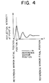
- Fig. 4 is a characteristic diagram showing variations in the reflection intensity at a point B with the movement of the reference mirror.
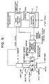
- Fig. 5 is a block diagram showing a three-dimensional curved surface shape measuring apparatus according to an embodiment of the invention.
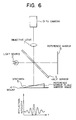
- Fig. 6 is a schematic diagram showing the light interference system in the apparatus of Fig. 5.
- Fig. 7 is a block diagram showing an example of the image composing circuit in Fig. 5.
- Fig. 3A is a schematic diagram for explaining the measuring principle of this invention
- Fig. 3B is a characteristic diagram showing the relation between the reference mirror position and the interference fringe pattern
- Fig. 4 is a characteristic diagram showing variations of the reflection intensity at a point B(see Fig. 3A) due to the movement of the reference mirror.
- an interference microscope includes a light source 2, a half mirror 3, a mount 4, a specimen 5, a reference mirror 6 and an objective lens 7.
- Numeral 9 designates a television camera, 9a a television monitor, and 14 an image composing circuit.
- the resulting interference fringes form a pattern such that the contrast becomes maximum at the position where the difference in optical path length between the specimen surface and the reference mirror surface is reduced to zero and the contrast is rapidly attenuated with increase in the optical path length difference.
- the reflection intensity at the point B varies as shown in Fig. 4 so that the reflection brightness becomes maximum when the reference mirror 6 arrives at a position A where its mirror image passes through the point B.
- This phenomenon means that while scanning the reference mirror 6 in the direction of the optical path to observe the reflection intensity at each of all the points in the field of view from moment to moment, if the image composing circuit 14 performs an image composing processing such that the value of each point is represented by the position of the reference mirror 6 at which the reflection intensity has the maximum value, the three-dimensional profile of the object to be measured can be measured as a pattern.
- Fig. 5 is a block diagram showing a three-dimensional curved surface shape measuring apparatus according to the embodiment of the invention and Fig. 6 is a schematic diagram for explaining the interference optical system in Fig. 5.
- Fig. 7 is a block diagram of the image composing circuit in Fig. 5.
- the light emitted from the light source 2 of the microscope 1 is divided into two parts by the half mirror 3 so that after these beams have been respectively reflected by the surface of specimen 5 placed on the mount 4 and the reference mirror 6, the reflected beams of light are again superimposed one upon another at the half mirror 3 and focussed by the objective lens 7 on the image pickup surface of the television camera 9 through the lens tube 8.
- this embodiment employs light of inferior coherency as the light source 2 so as to produce an interference fringe pattern such that as for example, the light intensity of the interference fringes becomes maximum at the position where the difference in optical path length between the surface of the specimen 5 and the plane of the reference mirror 6 is reduced to zero and the contrast of the interference fringes is rapidly attenuated with increase in the optical path length difference as shown in Fig. 4.
- the reference mirror 6 is arranged so that it makes a parallel movement in the optical axis direction through a reference mirror driving mechanism 11 which is controlled by a reference mirror position controller 10.
- a reference mirror driving mechanism 11 which is controlled by a reference mirror position controller 10.
- a shape measuring apparatus 12 is designed so that the scanning of the reference mirror 6 is controlled through the reference mirror position controller 10 and simultaneously the shape of the specimen is measured in accordance with the video signal generated from the television camera 9 and the reference mirror position signals generated from the reference mirror position controller 10.
- the apparatus 12 includes a sequence controller 13 for controlling the sequence of measuring operations and an image composing circuit 14 which will be described later and it has a function so that the video signal generated from the television camera 9 while scanning the reference mirror 6 is processed from moment to moment to form a composite image in which the value of each of picture elements in the image is represented by the position of the reference mirror 6 at instant that the point corresponding to that picture element has the maximum brightness.
- the sequence controller 13 applies a command to the reference mirror position controller 10 to set the reference mirror 6 in the initial position.
- the reference mirror position controller 10 sets the reference mirror 6 in the initial position through the reference mirror driving mechanism 11 and it also resets the mirror position signal to zero.
- the sequence controller 13 applies a drive start command to the reference mirror position controller 10 and it also applies a processing start command to the image composing circuit 14. Consequently, the reference mirror driving mechanism 11 scans the reference mirror 6 over such a range that there always occurs a moment at which the difference in optical path length between the specimen 5 and the reference mirror 6 is reduced to zero with respect to each of all the shape measuring points on the surface of the specimen 5. Simultaneously with the start of the scanning of the reference mirror 6, the image composing circuit 14 begins the processing of the video signal generated from the television camera 9 so that the previously mentioned image composing processing is performed during the time that the reference mirror 6 is scanned.
- the image composing circuit 14 completes the processing in response to the command from the sequence controller 13.
- the data corresponding to the three-dimensional profile of the specimen 5 is stored in the memory of the image composing circuit 14 and the data is suitably transferred to a higher-rank computer in response to the command therefrom.
- the image composing circuit 14 includes a maximum brightness image processing unit 15 for processing the video signal applied from the television camera 9 to compute the brightness of the instant that it becomes brightest for each of the picture elements, and a composite image processing unit 16 for performing an image composing processing in a manner that the value of each picture element is represented by the reference mirror position signal at the instant that the picture element has the maximum brightness in time. It also includes, for purposes of controlling the former circuits, a synchronizing circuit 17, a memory address generating circuit 18 and an output control circuit 19.
- the maximum brightness image processing unit 15 includes mainly a maximum brightness image memory 20 comprising a buffer memory for maximum brightness image processing purposes as well as an A/D converter circuit 21 responsive to the timing signals generated from the synchronizing circuit 17 to digitize the video signal by A/D conversion, a maximum brightness image memory control circuit 22 for controlling the reading and writing of data into the maximum brightness image memory addresses designated by the memory address generating circuit 18, a comparator circuit 23 for comparing the signal level of the image applied from the television camera 9 with the value of each picture element in the corresponding address of the maximum brightness imaga memory 20 to select and output greater-valued one of the two, and a switch circuit 24.
- the composite image processing unit 16 includes mainly a composite image memory 25 for storing the results of composite image processing as well as a composite image memory control circuit 26 having a function of responding to the output signal from the comparator circuit 23 of the maximum brightness image processing unit 15 so that when the input signal from the television camera 9 is greater than the value of the picture element at the corresponding address of the maximum brightness image memory 20, the current reference mirror position signal is written into the composite image memory 28.
- the image composing circuit 14 starts at the timing of beginning of the processing with the maximum brightness image memory 20 and the composite memory 25 being cleared to zero, so that while digitizing the video signal applied from the television camera 9 by the A/D converter circuit 21, the value of the video signal or the value of each of the picture elements is compared with the value of that picture element in the maximum brightness image memory 20 which corresponds to the position of the former picture element so that only when the value of the video signal is greater, the value of the picture element in the maximum brightness image memory 20 is updated by the value of the video signal and simultaneously the reference mirror position signal is written into the corresponding picture element of the composite image.
- the above-mentioned processing is performed so that the previously mentioned desired image is formed in the composite image memory 25 upon the completion of the processing.
- the thus processed composite image is transferred to the following processing circuit or a higher-rank computer through the output control circuit 19.
- the principle of the invention is also applicable to any other interference microscope such as the Mirau type or Linnik type, and also it is needless to say that the same principle holds by moving the mount 4 in the direction of the optical axis to scan the surface of a specimen instead of scanning the reference mirror and that the invention is not necessarily limited to the optical system of the above-described embodiment.
- the invention is applicable to any interferometer employing no microscope.
- any quantities can be effectively coded provided that these quantities are equivalent to the positions of the reference mirror.
Landscapes
- Physics & Mathematics (AREA)
- General Physics & Mathematics (AREA)
- Length Measuring Devices By Optical Means (AREA)
- Instruments For Measurement Of Length By Optical Means (AREA)
Claims (5)
- Verfahren zum Messen einer dreidimensional gekrümmten Oberflächenform, das die Verfahrensschritte aufweist:
Erzeugen von Interferenzstreifen, die an der Oberfläche eines Objektes (5) beobachtbar sind, das gemäß einer optischen Weglängendifferenz zwischen einem Lichtstrahl, der von der Oberfläche des zu vermessenden Objektes (5) reflektiert wird, und einem Lichtstrahl vermessen wird, der von einem ebenen Referenzreflektor (6) quer zu einer optischen Achse reflektiert wird;
Messen der Position des ebenen Referenzreflektors (6) oder einer Referenzoberfläche des zu vermessenden Objektes in der Richtung der optischen Achse oder eine Äquivalent-Größe zu der Position, während der ebene Reflektor (6) oder das Objekt (5) in der optischen Achsrichtung bewegt wird;
Aufnahme eines Musters von Interferenzstreifen, die auf der Oberfläche des zu vermessenden Objektes beobachtbar sind; gekennzeichnet durch die Verfahrensschritte:
Verarbeiten eins Videosignals von Augenblick zu Augenblick, das von dem aufgenommenen Muster erzeugt wird, um ein zusammengesetztes Abbild zu formen, in dem jedes von einer Anzahl von Bildelementen entsprechend den verschiedenen Positionen auf der Objektoberfläche einem Wert zugeordnet wird, der die Position des ebenen Referenzreflektors oder die Objektreferenzoberfläche in der optischen Achsrichtung oder eine Äquivalent-Größe dazu verkörpert, wenn jede der Positionen der Objektoberfläche seine maximale Helligkeit erreicht; und
Messen einer dreidimensional gekrümmten Oberflächenform des zu vermessenen Objektes gemäß dem zusammengesetzten Abbild. - Gerät zum Messen einer dreidimensional gekrümmten Oberfläche, das aufweist:
Eine Interferenzstreifen-Erzeugungseinrichtung (1) zum Erzeugen von Interferenzstreifen, die auf der Oberfläche eines Objektes (5) beobachtbar sind, das gemäß einer optischen Weglängendifferenz zwischen einem Lichtstrahl, der von der Oberfläche des zu vermessenden Objektes (5) reflektiert wird, und einem Lichtstrahl vermessen wird, der von einem ebenen Referenzreflektor (6) reflektiert wird;
Bewegungsvorrichtungen zum Bewegen des ebenen Referenzreflektors (6) oder des zu vermessenden Objektes in Richtung einer optischen Achse;
Positionsmeßeinrichtungen (10) zum Messen der Position des ebenen Referenzreflektors oder einer Referenzoberfläche des zu vermessenden Objektes in der optischen Achsrichtung oder einer Äquivalent-Größe dazu;
Abbildaufnahmeeinrichtungen (9) zur Aufnahme eines Musters von Interferenzstreifen, die auf der Oberfläche des zu vermessenden Objektes beobachtbar sind; gekennzeichnet durch:
Eine Abbildzusammensetz-Anordnung (14), die vorgesehen ist, um ein Videosignal von Augenblick zu Augenblick zu verarbeiten, das von der Abbildaufnahmeeinrichtung erzeugt wird, um ein zusammengesetztes Abbild zu erzeugen, in dem jedes von einer Anzahl von Bildelementen entsprechend den verschiedenen Positionen auf der Objektoberfläche einem Wert zugeordnet wird, der die Position des ebenen Referenzreflektors oder der Objektreferenzoberfläche in der optischen Wegrichtung oder einer Äquivalent-Größe dazu verkörpert, wenn eine Position auf der Objektoberfläche, die jedem Bildelement entspricht, ihre maximale Helligkeit erreicht;
wodurch eine dreidimensional gekrümmte Oberflächenform des zu vermessenden Objektes durch eine computerisierte Verarbeitung auf der Basis des zusammengesetzten Abbildes durchgeführt wird, das durch die Abbildzusammensetz-Anordnung (14) gebildet wird. - Gerät nach Anspruch 2, dadurch gekennzeichnet, daß die Abbildzusammensetz-Anordnung aufweist:
Maximumhelligkeits-Abbildspeichermittel (20) zum Speichern eines Maximumpegels des Videosignals für jedes Bildelement davon innerhalb einer vorbestimmten Zeitperiode;
Maximumhelligkeits-Verarbeitungseinrichtungen (15) zum Vergleichen des Videosignals und eines Signals, das in den Maximumhelligkeits-Abbildspeichermitteln gespeichert ist, in bezug auf jedes entsprechende Bildelement davon, um ein größerwertiges davon in den MaximumhelligkeitsAbbildspeichermitteln einzuschreiben:
Zusammensetzabbild-Speichermtitel (25), um für jedes Bildelement eine Größe des Synchronisationssignals oder einen Wert eines externen Eingangssignals zu speichern, wenn das Videosignal während einer vorbestimmten Zeitperiode den höchsten Pegel erreicht; und
Zusammensetzabbild-Verarbeitungseinrichtungen (16), wodurch für jedes Bildelement, für das die Maximumhelligkeits-Abbildverarbeitungseinrichtung betimmt, daß das Videosignal größer ist als das in den Maximumhelligkeits-Abbildspeichermitteln gespeicherte Signal, ein Zahlenwert des Synchronisationssignals oder ein Wert eines externen Eingangssignals in dem Augenblick der Bestimmung in die Zusammensetzabbild-Speichermittel (25) eingeschrieben wird. - Gerät nach Anspruch 2, dadurch gekennzeichnet, daß die Interferenzstreifen-Erzeugungseinrichtung ein Interferenzmikroskop aufweist.
- Gerät nach Anspruch 3, dadurch gekennzeichnet, daß die Interferenzstreifen-Erzeugungseinrichtung eine Lichtquelle mit geringer Kohärenz enthält.
Applications Claiming Priority (2)
| Application Number | Priority Date | Filing Date | Title |
|---|---|---|---|
| JP118201/88 | 1988-05-17 | ||
| JP63118201A JPH061167B2 (ja) | 1988-05-17 | 1988-05-17 | 3次元曲面形状の測定方法及び装置 |
Publications (3)
| Publication Number | Publication Date |
|---|---|
| EP0342289A2 EP0342289A2 (de) | 1989-11-23 |
| EP0342289A3 EP0342289A3 (en) | 1990-02-07 |
| EP0342289B1 true EP0342289B1 (de) | 1992-12-30 |
Family
ID=14730688
Family Applications (1)
| Application Number | Title | Priority Date | Filing Date |
|---|---|---|---|
| EP88309658A Expired - Lifetime EP0342289B1 (de) | 1988-05-17 | 1988-10-14 | Verfahren und Vorrichtung zum Messen einer dreidimensionalen gekrümmten Oberfläche |
Country Status (6)
| Country | Link |
|---|---|
| US (1) | US4874955A (de) |
| EP (1) | EP0342289B1 (de) |
| JP (1) | JPH061167B2 (de) |
| KR (1) | KR920010550B1 (de) |
| CA (1) | CA1294426C (de) |
| DE (1) | DE3877191T2 (de) |
Families Citing this family (20)
| Publication number | Priority date | Publication date | Assignee | Title |
|---|---|---|---|---|
| CA1313040C (en) * | 1988-03-31 | 1993-01-26 | Mitsuaki Uesugi | Method and apparatus for measuring a three-dimensional curved surface shape |
| US5175601A (en) * | 1991-10-15 | 1992-12-29 | Electro-Optical Information Systems | High-speed 3-D surface measurement surface inspection and reverse-CAD system |
| US5361308A (en) * | 1992-01-10 | 1994-11-01 | General Motors Corporation | 3-D measurement of cutting tool wear |
| US5319445A (en) * | 1992-09-08 | 1994-06-07 | Fitts John M | Hidden change distribution grating and use in 3D moire measurement sensors and CMM applications |
| US5543918A (en) * | 1995-01-06 | 1996-08-06 | International Business Machines Corporation | Through-the-lens confocal height measurement |
| US5627363A (en) * | 1995-02-16 | 1997-05-06 | Environmental Research Institute Of Michigan | System and method for three-dimensional imaging of opaque objects using frequency diversity and an opacity constraint |
| US6215269B1 (en) * | 1996-05-21 | 2001-04-10 | Kent Gregg | Method of exposing a path on a curved, or otherwise irregularly shaped, surface |
| DE19721884C1 (de) * | 1997-05-26 | 1998-06-04 | Bosch Gmbh Robert | Interferometrische Meßvorrichtung |
| AUPO810997A0 (en) | 1997-07-18 | 1997-08-14 | Lions Eye Institute Of Western Australia Incorporated, The | Method and apparatus for calibration of ablation lasers |
| JP3695188B2 (ja) * | 1998-12-21 | 2005-09-14 | 富士ゼロックス株式会社 | 形状計測装置および形状計測方法 |
| US6888640B2 (en) | 2000-02-04 | 2005-05-03 | Mario J. Spina | Body spatial dimension mapper |
| DE10040323C2 (de) * | 2000-08-17 | 2002-11-14 | Polytec Gesellschaft Fuer Analysen-, Mes- Und Regeltechnik Mbh & Co Kg | Vorrichtung und Verfahren zum optischen Vermessen des Höhenprofils einer Oberfläche |
| US7147338B2 (en) | 2001-04-09 | 2006-12-12 | Kent Gregg | Circuit on a curved, or otherwise irregularly shaped, surface, such as on a helmet to be worn on the head, including a fiber optic conductive path |
| DE502005006493D1 (de) * | 2004-10-29 | 2009-03-05 | Degudent Gmbh | Verfahren und vorrichtung zur erfassung von konturdaten und/oder optischen eigenschaften eines dreidimensionalen semitransparenten objekts |
| JP4197339B2 (ja) * | 2006-01-16 | 2008-12-17 | アンリツ株式会社 | 三次元形状測定装置 |
| JP5086655B2 (ja) * | 2007-02-06 | 2012-11-28 | 株式会社トプコン | 三次元形状測定装置及び三次元形状測定方法 |
| JP5342178B2 (ja) * | 2008-06-10 | 2013-11-13 | 株式会社ニコンインステック | 形状測定装置およびその形状測定方法 |
| KR101458997B1 (ko) | 2014-06-09 | 2014-11-07 | 김호환 | 리닉 간섭계의 기준미러 변환장치 |
| CN113251943A (zh) * | 2020-02-12 | 2021-08-13 | 三营超精密光电(晋城)有限公司 | 基于光干涉的测量系统及方法 |
| CN112388159A (zh) * | 2020-10-29 | 2021-02-23 | 青岛理工大学 | 分数傅里叶全息飞秒激光三维并行加工、监测系统及方法 |
Family Cites Families (5)
| Publication number | Priority date | Publication date | Assignee | Title |
|---|---|---|---|---|
| JPH061164B2 (ja) * | 1985-01-31 | 1994-01-05 | 伍良 松本 | 立体形状測定装置 |
| JPH0654221B2 (ja) * | 1985-04-12 | 1994-07-20 | 株式会社日立製作所 | 段差測定装置およびその方法 |
| US4818110A (en) * | 1986-05-06 | 1989-04-04 | Kla Instruments Corporation | Method and apparatus of using a two beam interference microscope for inspection of integrated circuits and the like |
| US4794550A (en) * | 1986-10-15 | 1988-12-27 | Eastman Kodak Company | Extended-range moire contouring |
| JPH0611106A (ja) * | 1992-06-25 | 1994-01-21 | Nippon Steel Corp | 加熱炉の燃焼方法 |
-
1988
- 1988-05-17 JP JP63118201A patent/JPH061167B2/ja not_active Expired - Lifetime
- 1988-09-30 KR KR1019880012739A patent/KR920010550B1/ko not_active Expired
- 1988-10-07 CA CA000579657A patent/CA1294426C/en not_active Expired - Lifetime
- 1988-10-14 DE DE8888309658T patent/DE3877191T2/de not_active Expired - Fee Related
- 1988-10-14 EP EP88309658A patent/EP0342289B1/de not_active Expired - Lifetime
- 1988-10-17 US US07/258,603 patent/US4874955A/en not_active Expired - Lifetime
Also Published As
| Publication number | Publication date |
|---|---|
| DE3877191T2 (de) | 1993-05-19 |
| EP0342289A3 (en) | 1990-02-07 |
| CA1294426C (en) | 1992-01-21 |
| EP0342289A2 (de) | 1989-11-23 |
| JPH061167B2 (ja) | 1994-01-05 |
| JPH01288702A (ja) | 1989-11-21 |
| US4874955A (en) | 1989-10-17 |
| KR920010550B1 (ko) | 1992-12-05 |
| DE3877191D1 (de) | 1993-02-11 |
| KR890017521A (ko) | 1989-12-16 |
Similar Documents
| Publication | Publication Date | Title |
|---|---|---|
| EP0342289B1 (de) | Verfahren und Vorrichtung zum Messen einer dreidimensionalen gekrümmten Oberfläche | |
| US5102223A (en) | Method and apparatus for measuring a three-dimensional curved surface shape | |
| JP3305598B2 (ja) | 走査遠隔結像法及びシステム | |
| US4961155A (en) | XYZ coordinates measuring system | |
| US9881400B2 (en) | Method for measuring a high accuracy height map of a test surface | |
| US4585350A (en) | Pulsed robotic inspection | |
| US5175601A (en) | High-speed 3-D surface measurement surface inspection and reverse-CAD system | |
| US5307151A (en) | Method and apparatus for three-dimensional optical measurement of object surfaces | |
| US6268923B1 (en) | Optical method and system for measuring three-dimensional surface topography of an object having a surface contour | |
| US6181425B1 (en) | Method and system for high speed measuring of microscopic targets | |
| US4838696A (en) | Pulsed robotic inspection | |
| US5319442A (en) | Optical inspection probe | |
| JPS63501526A (ja) | 高速三次元表面デイジタイザ | |
| US6697163B2 (en) | Shape measuring apparatus | |
| US4847509A (en) | Method and apparatus for measuring the diameter of a running elongate object such as an optical fiber | |
| JP2535561B2 (ja) | 三次元座標測定装置 | |
| KR920010547B1 (ko) | 3차원 곡면 형상의 측정방법 및 장치 | |
| JP2942972B2 (ja) | 干渉計測システム | |
| KR920010548B1 (ko) | 3차원 곡면 형상의 측정방법 및 장치 | |
| JP2626611B2 (ja) | 物体形状測定方法 | |
| JP2017151062A (ja) | 表面形状測定装置及び表面形状測定方法 | |
| JPH01235807A (ja) | 深さ測定装置 | |
| JPH0843017A (ja) | 走査型光学顕微鏡 | |
| JP3018887B2 (ja) | 三次元形状測定装置 | |
| JPH085449Y2 (ja) | 顕微鏡 |
Legal Events
| Date | Code | Title | Description |
|---|---|---|---|
| PUAI | Public reference made under article 153(3) epc to a published international application that has entered the european phase |
Free format text: ORIGINAL CODE: 0009012 |
|
| AK | Designated contracting states |
Kind code of ref document: A2 Designated state(s): DE FR GB IT |
|
| PUAL | Search report despatched |
Free format text: ORIGINAL CODE: 0009013 |
|
| AK | Designated contracting states |
Kind code of ref document: A3 Designated state(s): DE FR GB IT |
|
| 17P | Request for examination filed |
Effective date: 19900725 |
|
| 17Q | First examination report despatched |
Effective date: 19910627 |
|
| GRAA | (expected) grant |
Free format text: ORIGINAL CODE: 0009210 |
|
| ITF | It: translation for a ep patent filed | ||
| AK | Designated contracting states |
Kind code of ref document: B1 Designated state(s): DE FR GB IT |
|
| REF | Corresponds to: |
Ref document number: 3877191 Country of ref document: DE Date of ref document: 19930211 |
|
| ET | Fr: translation filed | ||
| PLBE | No opposition filed within time limit |
Free format text: ORIGINAL CODE: 0009261 |
|
| STAA | Information on the status of an ep patent application or granted ep patent |
Free format text: STATUS: NO OPPOSITION FILED WITHIN TIME LIMIT |
|
| 26N | No opposition filed | ||
| PG25 | Lapsed in a contracting state [announced via postgrant information from national office to epo] |
Ref country code: FR Effective date: 19940630 |
|
| REG | Reference to a national code |
Ref country code: FR Ref legal event code: ST |
|
| PGFP | Annual fee paid to national office [announced via postgrant information from national office to epo] |
Ref country code: GB Payment date: 19971006 Year of fee payment: 10 |
|
| PGFP | Annual fee paid to national office [announced via postgrant information from national office to epo] |
Ref country code: DE Payment date: 19971017 Year of fee payment: 10 |
|
| PG25 | Lapsed in a contracting state [announced via postgrant information from national office to epo] |
Ref country code: GB Free format text: LAPSE BECAUSE OF NON-PAYMENT OF DUE FEES Effective date: 19981014 |
|
| GBPC | Gb: european patent ceased through non-payment of renewal fee |
Effective date: 19981014 |
|
| PG25 | Lapsed in a contracting state [announced via postgrant information from national office to epo] |
Ref country code: DE Free format text: LAPSE BECAUSE OF NON-PAYMENT OF DUE FEES Effective date: 19990803 |
|
| PG25 | Lapsed in a contracting state [announced via postgrant information from national office to epo] |
Ref country code: IT Free format text: LAPSE BECAUSE OF NON-PAYMENT OF DUE FEES Effective date: 20051014 |