EP0342018B1 - Dispositifs laser à semi-conducteur et méthode pour leur fabrication - Google Patents
Dispositifs laser à semi-conducteur et méthode pour leur fabrication Download PDFInfo
- Publication number
- EP0342018B1 EP0342018B1 EP89304757A EP89304757A EP0342018B1 EP 0342018 B1 EP0342018 B1 EP 0342018B1 EP 89304757 A EP89304757 A EP 89304757A EP 89304757 A EP89304757 A EP 89304757A EP 0342018 B1 EP0342018 B1 EP 0342018B1
- Authority
- EP
- European Patent Office
- Prior art keywords
- layers
- layer
- semiconductor laser
- growth
- carrier injection
- Prior art date
- Legal status (The legal status is an assumption and is not a legal conclusion. Google has not performed a legal analysis and makes no representation as to the accuracy of the status listed.)
- Expired - Lifetime
Links
- 238000000034 method Methods 0.000 title claims description 29
- 230000008569 process Effects 0.000 title claims description 19
- 239000004065 semiconductor Substances 0.000 title claims description 13
- 239000000758 substrate Substances 0.000 claims description 20
- 238000002347 injection Methods 0.000 claims description 19
- 239000007924 injection Substances 0.000 claims description 19
- 238000005530 etching Methods 0.000 claims description 13
- 239000013078 crystal Substances 0.000 claims description 9
- 125000005842 heteroatom Chemical group 0.000 claims description 6
- 239000012808 vapor phase Substances 0.000 claims description 6
- 239000000463 material Substances 0.000 claims description 4
- 229910016920 AlzGa1−z Inorganic materials 0.000 claims description 3
- 239000010410 layer Substances 0.000 description 90
- 229910001218 Gallium arsenide Inorganic materials 0.000 description 10
- 230000004888 barrier function Effects 0.000 description 8
- 230000000903 blocking effect Effects 0.000 description 6
- VEXZGXHMUGYJMC-UHFFFAOYSA-N Hydrochloric acid Chemical compound Cl VEXZGXHMUGYJMC-UHFFFAOYSA-N 0.000 description 4
- 239000000969 carrier Substances 0.000 description 4
- 239000007789 gas Substances 0.000 description 4
- 229910000041 hydrogen chloride Inorganic materials 0.000 description 4
- IXCSERBJSXMMFS-UHFFFAOYSA-N hydrogen chloride Substances Cl.Cl IXCSERBJSXMMFS-UHFFFAOYSA-N 0.000 description 4
- 229910004205 SiNX Inorganic materials 0.000 description 3
- 229910000980 Aluminium gallium arsenide Inorganic materials 0.000 description 2
- KRHYYFGTRYWZRS-UHFFFAOYSA-N Fluorane Chemical compound F KRHYYFGTRYWZRS-UHFFFAOYSA-N 0.000 description 2
- VYPSYNLAJGMNEJ-UHFFFAOYSA-N Silicium dioxide Chemical compound O=[Si]=O VYPSYNLAJGMNEJ-UHFFFAOYSA-N 0.000 description 2
- 239000004411 aluminium Substances 0.000 description 2
- 229910052782 aluminium Inorganic materials 0.000 description 2
- XAGFODPZIPBFFR-UHFFFAOYSA-N aluminium Chemical compound [Al] XAGFODPZIPBFFR-UHFFFAOYSA-N 0.000 description 2
- 230000015572 biosynthetic process Effects 0.000 description 2
- 229910052751 metal Inorganic materials 0.000 description 2
- 239000002184 metal Substances 0.000 description 2
- 230000010355 oscillation Effects 0.000 description 2
- 230000001681 protective effect Effects 0.000 description 2
- 230000005855 radiation Effects 0.000 description 2
- GYHNNYVSQQEPJS-UHFFFAOYSA-N Gallium Chemical compound [Ga] GYHNNYVSQQEPJS-UHFFFAOYSA-N 0.000 description 1
- 229910019142 PO4 Inorganic materials 0.000 description 1
- RBFQJDQYXXHULB-UHFFFAOYSA-N arsane Chemical compound [AsH3] RBFQJDQYXXHULB-UHFFFAOYSA-N 0.000 description 1
- 229910052785 arsenic Inorganic materials 0.000 description 1
- RQNWIZPPADIBDY-UHFFFAOYSA-N arsenic atom Chemical compound [As] RQNWIZPPADIBDY-UHFFFAOYSA-N 0.000 description 1
- 239000007853 buffer solution Substances 0.000 description 1
- 230000008859 change Effects 0.000 description 1
- 238000005229 chemical vapour deposition Methods 0.000 description 1
- 238000005253 cladding Methods 0.000 description 1
- 229910052681 coesite Inorganic materials 0.000 description 1
- 229910052906 cristobalite Inorganic materials 0.000 description 1
- 230000003247 decreasing effect Effects 0.000 description 1
- 230000002542 deteriorative effect Effects 0.000 description 1
- 230000000694 effects Effects 0.000 description 1
- 238000010292 electrical insulation Methods 0.000 description 1
- 229910052733 gallium Inorganic materials 0.000 description 1
- 239000011521 glass Substances 0.000 description 1
- 238000011065 in-situ storage Methods 0.000 description 1
- 239000007791 liquid phase Substances 0.000 description 1
- 238000004519 manufacturing process Methods 0.000 description 1
- 239000000155 melt Substances 0.000 description 1
- 235000021317 phosphate Nutrition 0.000 description 1
- 150000003013 phosphoric acid derivatives Chemical class 0.000 description 1
- 230000006798 recombination Effects 0.000 description 1
- 238000005215 recombination Methods 0.000 description 1
- 230000009467 reduction Effects 0.000 description 1
- 230000004044 response Effects 0.000 description 1
- 239000000377 silicon dioxide Substances 0.000 description 1
- 235000012239 silicon dioxide Nutrition 0.000 description 1
- 239000000243 solution Substances 0.000 description 1
- 229910052682 stishovite Inorganic materials 0.000 description 1
- 239000002344 surface layer Substances 0.000 description 1
- 230000007704 transition Effects 0.000 description 1
- 229910052905 tridymite Inorganic materials 0.000 description 1
- JLTRXTDYQLMHGR-UHFFFAOYSA-N trimethylaluminium Chemical compound C[Al](C)C JLTRXTDYQLMHGR-UHFFFAOYSA-N 0.000 description 1
- XCZXGTMEAKBVPV-UHFFFAOYSA-N trimethylgallium Chemical compound C[Ga](C)C XCZXGTMEAKBVPV-UHFFFAOYSA-N 0.000 description 1
- 238000007740 vapor deposition Methods 0.000 description 1
- 238000001947 vapour-phase growth Methods 0.000 description 1
- 238000001039 wet etching Methods 0.000 description 1
Images

Classifications
-
- H—ELECTRICITY
- H01—ELECTRIC ELEMENTS
- H01S—DEVICES USING THE PROCESS OF LIGHT AMPLIFICATION BY STIMULATED EMISSION OF RADIATION [LASER] TO AMPLIFY OR GENERATE LIGHT; DEVICES USING STIMULATED EMISSION OF ELECTROMAGNETIC RADIATION IN WAVE RANGES OTHER THAN OPTICAL
- H01S5/00—Semiconductor lasers
- H01S5/30—Structure or shape of the active region; Materials used for the active region
-
- B—PERFORMING OPERATIONS; TRANSPORTING
- B82—NANOTECHNOLOGY
- B82Y—SPECIFIC USES OR APPLICATIONS OF NANOSTRUCTURES; MEASUREMENT OR ANALYSIS OF NANOSTRUCTURES; MANUFACTURE OR TREATMENT OF NANOSTRUCTURES
- B82Y20/00—Nanooptics, e.g. quantum optics or photonic crystals
-
- H—ELECTRICITY
- H01—ELECTRIC ELEMENTS
- H01S—DEVICES USING THE PROCESS OF LIGHT AMPLIFICATION BY STIMULATED EMISSION OF RADIATION [LASER] TO AMPLIFY OR GENERATE LIGHT; DEVICES USING STIMULATED EMISSION OF ELECTROMAGNETIC RADIATION IN WAVE RANGES OTHER THAN OPTICAL
- H01S5/00—Semiconductor lasers
- H01S5/20—Structure or shape of the semiconductor body to guide the optical wave ; Confining structures perpendicular to the optical axis, e.g. index or gain guiding, stripe geometry, broad area lasers, gain tailoring, transverse or lateral reflectors, special cladding structures, MQW barrier reflection layers
- H01S5/22—Structure or shape of the semiconductor body to guide the optical wave ; Confining structures perpendicular to the optical axis, e.g. index or gain guiding, stripe geometry, broad area lasers, gain tailoring, transverse or lateral reflectors, special cladding structures, MQW barrier reflection layers having a ridge or stripe structure
- H01S5/2203—Structure or shape of the semiconductor body to guide the optical wave ; Confining structures perpendicular to the optical axis, e.g. index or gain guiding, stripe geometry, broad area lasers, gain tailoring, transverse or lateral reflectors, special cladding structures, MQW barrier reflection layers having a ridge or stripe structure with a transverse junction stripe [TJS] structure
-
- H—ELECTRICITY
- H01—ELECTRIC ELEMENTS
- H01S—DEVICES USING THE PROCESS OF LIGHT AMPLIFICATION BY STIMULATED EMISSION OF RADIATION [LASER] TO AMPLIFY OR GENERATE LIGHT; DEVICES USING STIMULATED EMISSION OF ELECTROMAGNETIC RADIATION IN WAVE RANGES OTHER THAN OPTICAL
- H01S5/00—Semiconductor lasers
- H01S5/20—Structure or shape of the semiconductor body to guide the optical wave ; Confining structures perpendicular to the optical axis, e.g. index or gain guiding, stripe geometry, broad area lasers, gain tailoring, transverse or lateral reflectors, special cladding structures, MQW barrier reflection layers
- H01S5/22—Structure or shape of the semiconductor body to guide the optical wave ; Confining structures perpendicular to the optical axis, e.g. index or gain guiding, stripe geometry, broad area lasers, gain tailoring, transverse or lateral reflectors, special cladding structures, MQW barrier reflection layers having a ridge or stripe structure
- H01S5/227—Buried mesa structure ; Striped active layer
-
- H—ELECTRICITY
- H01—ELECTRIC ELEMENTS
- H01S—DEVICES USING THE PROCESS OF LIGHT AMPLIFICATION BY STIMULATED EMISSION OF RADIATION [LASER] TO AMPLIFY OR GENERATE LIGHT; DEVICES USING STIMULATED EMISSION OF ELECTROMAGNETIC RADIATION IN WAVE RANGES OTHER THAN OPTICAL
- H01S5/00—Semiconductor lasers
- H01S5/30—Structure or shape of the active region; Materials used for the active region
- H01S5/32—Structure or shape of the active region; Materials used for the active region comprising PN junctions, e.g. hetero- or double- heterostructures
-
- H—ELECTRICITY
- H01—ELECTRIC ELEMENTS
- H01S—DEVICES USING THE PROCESS OF LIGHT AMPLIFICATION BY STIMULATED EMISSION OF RADIATION [LASER] TO AMPLIFY OR GENERATE LIGHT; DEVICES USING STIMULATED EMISSION OF ELECTROMAGNETIC RADIATION IN WAVE RANGES OTHER THAN OPTICAL
- H01S5/00—Semiconductor lasers
- H01S5/30—Structure or shape of the active region; Materials used for the active region
- H01S5/34—Structure or shape of the active region; Materials used for the active region comprising quantum well or superlattice structures, e.g. single quantum well [SQW] lasers, multiple quantum well [MQW] lasers or graded index separate confinement heterostructure [GRINSCH] lasers
- H01S5/343—Structure or shape of the active region; Materials used for the active region comprising quantum well or superlattice structures, e.g. single quantum well [SQW] lasers, multiple quantum well [MQW] lasers or graded index separate confinement heterostructure [GRINSCH] lasers in AIIIBV compounds, e.g. AlGaAs-laser, InP-based laser
- H01S5/34313—Structure or shape of the active region; Materials used for the active region comprising quantum well or superlattice structures, e.g. single quantum well [SQW] lasers, multiple quantum well [MQW] lasers or graded index separate confinement heterostructure [GRINSCH] lasers in AIIIBV compounds, e.g. AlGaAs-laser, InP-based laser with a well layer having only As as V-compound, e.g. AlGaAs, InGaAs
-
- H—ELECTRICITY
- H01—ELECTRIC ELEMENTS
- H01S—DEVICES USING THE PROCESS OF LIGHT AMPLIFICATION BY STIMULATED EMISSION OF RADIATION [LASER] TO AMPLIFY OR GENERATE LIGHT; DEVICES USING STIMULATED EMISSION OF ELECTROMAGNETIC RADIATION IN WAVE RANGES OTHER THAN OPTICAL
- H01S5/00—Semiconductor lasers
- H01S5/04—Processes or apparatus for excitation, e.g. pumping, e.g. by electron beams
- H01S5/042—Electrical excitation ; Circuits therefor
- H01S5/0421—Electrical excitation ; Circuits therefor characterised by the semiconducting contacting layers
- H01S5/0422—Electrical excitation ; Circuits therefor characterised by the semiconducting contacting layers with n- and p-contacts on the same side of the active layer
- H01S5/0424—Electrical excitation ; Circuits therefor characterised by the semiconducting contacting layers with n- and p-contacts on the same side of the active layer lateral current injection
-
- H—ELECTRICITY
- H01—ELECTRIC ELEMENTS
- H01S—DEVICES USING THE PROCESS OF LIGHT AMPLIFICATION BY STIMULATED EMISSION OF RADIATION [LASER] TO AMPLIFY OR GENERATE LIGHT; DEVICES USING STIMULATED EMISSION OF ELECTROMAGNETIC RADIATION IN WAVE RANGES OTHER THAN OPTICAL
- H01S5/00—Semiconductor lasers
- H01S5/20—Structure or shape of the semiconductor body to guide the optical wave ; Confining structures perpendicular to the optical axis, e.g. index or gain guiding, stripe geometry, broad area lasers, gain tailoring, transverse or lateral reflectors, special cladding structures, MQW barrier reflection layers
- H01S5/22—Structure or shape of the semiconductor body to guide the optical wave ; Confining structures perpendicular to the optical axis, e.g. index or gain guiding, stripe geometry, broad area lasers, gain tailoring, transverse or lateral reflectors, special cladding structures, MQW barrier reflection layers having a ridge or stripe structure
- H01S5/227—Buried mesa structure ; Striped active layer
- H01S5/2275—Buried mesa structure ; Striped active layer mesa created by etching
-
- H—ELECTRICITY
- H01—ELECTRIC ELEMENTS
- H01S—DEVICES USING THE PROCESS OF LIGHT AMPLIFICATION BY STIMULATED EMISSION OF RADIATION [LASER] TO AMPLIFY OR GENERATE LIGHT; DEVICES USING STIMULATED EMISSION OF ELECTROMAGNETIC RADIATION IN WAVE RANGES OTHER THAN OPTICAL
- H01S5/00—Semiconductor lasers
- H01S5/30—Structure or shape of the active region; Materials used for the active region
- H01S5/34—Structure or shape of the active region; Materials used for the active region comprising quantum well or superlattice structures, e.g. single quantum well [SQW] lasers, multiple quantum well [MQW] lasers or graded index separate confinement heterostructure [GRINSCH] lasers
- H01S5/343—Structure or shape of the active region; Materials used for the active region comprising quantum well or superlattice structures, e.g. single quantum well [SQW] lasers, multiple quantum well [MQW] lasers or graded index separate confinement heterostructure [GRINSCH] lasers in AIIIBV compounds, e.g. AlGaAs-laser, InP-based laser
- H01S5/34313—Structure or shape of the active region; Materials used for the active region comprising quantum well or superlattice structures, e.g. single quantum well [SQW] lasers, multiple quantum well [MQW] lasers or graded index separate confinement heterostructure [GRINSCH] lasers in AIIIBV compounds, e.g. AlGaAs-laser, InP-based laser with a well layer having only As as V-compound, e.g. AlGaAs, InGaAs
- H01S5/3432—Structure or shape of the active region; Materials used for the active region comprising quantum well or superlattice structures, e.g. single quantum well [SQW] lasers, multiple quantum well [MQW] lasers or graded index separate confinement heterostructure [GRINSCH] lasers in AIIIBV compounds, e.g. AlGaAs-laser, InP-based laser with a well layer having only As as V-compound, e.g. AlGaAs, InGaAs the whole junction comprising only (AI)GaAs
Definitions
- the present invention relates to a process for making an embedded type semiconductor laser device.
- Figure 2 illustrates a typical structure of a conventional semiconductor laser device in which the transverse mode is controlled by the provision of an embedded layer.
- reference numeral 22 stands for a semi-insulating substrate, 23 a lower clad layer, 24 an active layer, 25 an upper clad layer, 26 a p-type carrier injection layer, 27 a blocking layer, 28 an n-type carrier injection layer, and 29 and 30 electrodes.
- the laser device shown in Figure 2 is of the structure that carriers are transversely injected in the active layer.
- the lower clad layer 23 of Al x Ga 1-x As, the active layer 24 of Al y Ga 1-y As and the upper clad layer 25 of Al x Ga 1-x As, provided that x > y, are laminated on the semi-insulating substrate 22 of GaAs in that order.
- the active layer 24 may be not only of the above structure but also of a singlet or multiplet quantum well structure or a multiplet active layer structure thereof.
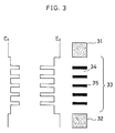
- Figure 3 is a view for illustrating a conventional multiplet quantum well structure.
- the thickness of the active layer is 20 nm or below, electrons occupy only limited levels due to the resulting quantum effect. For that reason, transition occurs on the thus limited levels so that the efficiency of radiation is increased, resulting in a decrease in threshold value currents.
- the multiplet quantum well structure makes use of such phenomena. As illustrated, a very small thickness is given to an active layer 33 formed between upper and lower clad layers 31 and 32, while barrier layers 34 of AlGaAs and quantum wells 35 of GaAs are repeatedly formed. To effectively confine light in the active layer, the mixed crystal ratio of Al of the barrier layers is smaller than that of the clad layers.
- the thickness of barrier layers and the mixed crystal ratio of barrier layers (generally, the number of wells is 5, the thickness of barrier layers is 6 to 20 nm and the Al to As ratio of barrier layers is 0.2 to 0.3). This is because in the case of the structure where currents flow in the longitudinal direction, there is a change in the injection of carriers in the upper and lower quantum wells.
- the transverse junction type laser device is freed of such limitations. Thus, an energy band structure of a conduction band Ec and a valence band Ev is obtained, as illustrated.
- Carriers are injected in the quantum wells, so that radiation takes place due to the recombination of electrons with holes, and the coherency of output light is maintained by reason that the quantum wells interact. It is noted that the reason why the space between the clad layer and the first quantum well is increased is to prevent the similarity of other quantum well to the energy band structure from deteriorating because of the energy level of the clad layer being high. By using the quantum wells for the active layer, it is also possible to obtain a very decreased inter-electrode capacity.
- regions for embedding p- and n-type carrier injection layers 26 and 28 are formed by the LPE (liquid-phase epitaxial) technique.
- a blocking layer 27 is provided to prevent any leak from occurring between the p- and n-type carrier injection layers 2 through a substrate.
- JP-A-60-235491 discloses an embedded (transverse junction) semiconductor laser composed of a substrate; a mesa form double heterostructure in which an active layer is sandwiched between upper and lower Al x Ga 1-x As clad layers with an Al mole fraction o ⁇ x ⁇ 1; and n+- and n ⁇ -type contact layers having electrodes on their surfaces.
- JP-A-61-079284 discloses a transverse junction (quantum-well active layer) semiconductor laser comprising two high specific resistance cladding layers formed of Al x Ga 1-x As, 0.3 ⁇ x ⁇ 0.8 which enclose an active layer and barrier layers.
- JP-A-58-225680 discloses a transverse junction (quantum-well active layer) semiconductor laser similar to that made according to the process of this invention, but having no n+- and n ⁇ -type contact layers provided between the carrier injection layers and the corresponding electrodes.
- An object of the present invention is to provide a process to make an embedded type of semiconductor laser device by embedding and regrowing carrier injection layers on Al x Ga 1-x As wherein 0.3 ⁇ x ⁇ 0.85 with the use of crystal growth processes capable of growing ternary or more multiple system crystals containing aluminium, by the MO-VPE (organic metal vapor-phase epitaxial) technique or the MO-MBE (organic metal molecular beam epitaxial) technique.
- MO-VPE organic metal vapor-phase epitaxial
- MO-MBE organic metal molecular beam epitaxial
- a process for making a semiconductor laser device comprising a semi-insulating substrate; a mesa-form double hetero structure in which an active layer of Al y Ga 1-y As is sandwiched between upper and lower clad layers, each having a high specific resistance and being formed of Al x Ga 1-x As, provided that 0.3 ⁇ x ⁇ 0.85, 0 ⁇ y ⁇ 0.45 and 0 ⁇ y ⁇ x; n- and p- type carrier injection layers of Al z Ga 1-z As and between which said double hetero structure is interposed, provided that y ⁇ z ⁇ x; and n+- and p+-type contact layers having electrodes formed on their surfaces; in which process mesa etching is applied to halfway through the lower clad layer and afterwards the carrier injection layers are embedded and re-grown on said lower clad layer of Al x Ga 1-x Ga with the use of the crystal growth process MO-VPE or MO-MBE where the material supply sources are all provided by
- reference numeral 1 stands for a semi-insulating substrate, 2 a lower clad layer, 3 an active layer, 4 an upper clad layer, 5 a p-type carrier injection layer, 6 a p+-contact layer, 7 an n-type carrier injection layer, 8 an n+-contact layer and 9 and 10 electrodes.
- a double hetero (DH) structure including the Al y Ga 1-y As active layer 3 having a thickness of 3 nm to 500 nm, preferably 10 to 300 nm, which is sandwiched between the Al x Ga 1-x As clad layers 2 and 4, provided that 0.3 ⁇ x ⁇ 0.85, 0 ⁇ y ⁇ 0.45 and 0 ⁇ y ⁇ x.
- the upper and lower clad layers 4 and 2 have a thickness of 0.5 to 2 ⁇ m and 1 to 5 ⁇ m, respectively.
- the substrate may be any amorphous substrate of glass or any low-resistance substrate, if the vapor-phase growth of Al y Ga 1-y As takes place thereon.
- the structure of the active layer 3 is not limited to the above type, and may be of a singlet or multiplet quantum well type. Alternatively, the active layer 3 may be formed of a laminate of two or more of such active layers.
- mesa etching is applied to halfway through the lower clad layer 2 of Al x Ga 1-x As (0.3 ⁇ x ⁇ 0.85), leaving behind a portion of about 0.2 to 1 ⁇ m, to form a p-side (11) or n-side (12) carrier injection region on Al x Ga 1-x As.
- the carrier concentration may be about 5 ⁇ 1017 to 2 ⁇ 1018cm ⁇ 3 for the p-type carrier injection layer 5, about 2 ⁇ 1018 to 5 ⁇ 1019cm ⁇ 3 for the p+-contact layer 6, about 5 ⁇ 1017 to 2 ⁇ 1018cm ⁇ 3 for the n-type carrier injection layer 7 and about 1 ⁇ 1018 to 3 ⁇ 1018cm ⁇ 3 for the n+-contact layer 8, as measured by the Van der Pauw's method.
- the other region 12 or 11 is subjected to mesa etching and embedding growth. Regions 11 and 12 comprising the embedded layers 5, 7 and the contact layers 6, 8 are formed in this manner.
- the SiN x film, now applied with a resist, is exposed to ultraviolet rays to pattern an one-side embedding region, and is then windowed with a hydrofluoric acid buffer solution (1HF:24NH4F) followed by the removal of the resist. Thereafter, about 1.7- ⁇ m mesa etching is applied to halfway through the lower clad layer of undoped Al 0.42 Ga 0.50 As with an aqueous etching solution containing phosphates in excess (1H3PO4:1H2O2:3HOC2H5C2H5OH).
- (epi-side) AuZn/Ni/Au (surface side) and (epi-side) AuZn/Ni/Au (surface side) are respectively vapor-deposited on the surfaces of the n- and p-side regions.
- vapor-phase mesa etching may be carried out in place of wet etching, while a gas such as HCl is admitted in the reactor using the above protective film, immediately followed by embedding and re-growth.
- a gas such as HCl
- the transverse junction type of embedded hetero structure shown in Figure 1 was continuously oscillated in the form of a quintuplet quantum well structure at normal temperature, a resonator wavelength of 160 ⁇ m, an active layer's width of 2.0 ⁇ m, an active layer's thickness of 230 nm, a barrier layer's thickness of 19 nm and a quantum well's thickness of 11 nm.
- output light of 1.8 mW at an oscillation wavelength of 868 to 870 nm was obtained at a threshold value current of 9.5 mA, a forward inter-electrode voltage of 34 ⁇ and 14 mA.
- a value as small as 0.042 pF (at zero bias time) was obtained.
- the carrier injection layers are formed on the clad layers of Al x Ga 1-x As of high resistance by embedding and re-growth with the use of crystal growth techniques such as MO-VPE or MO-MBE where material supply sources are all provided by gas sources, whereby:
Landscapes
- Physics & Mathematics (AREA)
- Optics & Photonics (AREA)
- Condensed Matter Physics & Semiconductors (AREA)
- General Physics & Mathematics (AREA)
- Electromagnetism (AREA)
- Engineering & Computer Science (AREA)
- Chemical & Material Sciences (AREA)
- Geometry (AREA)
- Nanotechnology (AREA)
- Life Sciences & Earth Sciences (AREA)
- Biophysics (AREA)
- Crystallography & Structural Chemistry (AREA)
- Semiconductor Lasers (AREA)
- Recrystallisation Techniques (AREA)
Claims (2)
- Procédé pour fabriquer un dispositif laser à semi-conducteur comprenant un substrat semi-isolant (1); une double hétérostructure de forme mésa dans laquelle une couche active (3) de AlyGa1-yAs est prise en sandwich entre des couches enveloppes supérieure (4) et inférieure (2), chacune ayant une résistance spécifique élevée et étant formée de AlxGa1-xAs, pourvu que 0,3 < x < 0,85, 0 < y < 0,45 et 0 < y < x; des couches d'injection de porteurs de type n et p (5,7) de AlzGa1-zAs et entre lesquelles est interposée ladite double hétérostructure (2,3,4), pourvu que y < z < x; et des couches de contact de type n et p (6,8) sur les surfaces desquelles sont formées des électrodes (9,10),
procédé dans lequel on effectue une attaque en mode mésa jusqu'à mi-distance à travers la couche enveloppe inférieure (2) et ensuite les couches d'injection de porteurs (5,7) sont incorporées et soumises à une re-croissance sur ladite couche incorporée inférieure de AlxGa1-xAs, en utilisant un procédé de croissance des cristaux MO-VPE ou MO-MBE, dans lequel les sources de fourniture de matériaux sont toutes des sources de gaz, et dans lequel, juste avant la re-croissance, on enlève un film d'oxyde de la surface de AlxGa1-xAs par attaque en phase vapeur. - Procédé selon la revendication 1, qui comporte une jonction p-n dans la direction transversale.
Applications Claiming Priority (2)
| Application Number | Priority Date | Filing Date | Title |
|---|---|---|---|
| JP63113898A JPH0831658B2 (ja) | 1988-05-11 | 1988-05-11 | 半導体レーザ及びその製造方法 |
| JP113898/88 | 1988-05-11 |
Publications (3)
| Publication Number | Publication Date |
|---|---|
| EP0342018A2 EP0342018A2 (fr) | 1989-11-15 |
| EP0342018A3 EP0342018A3 (en) | 1990-03-14 |
| EP0342018B1 true EP0342018B1 (fr) | 1993-12-22 |
Family
ID=14623918
Family Applications (1)
| Application Number | Title | Priority Date | Filing Date |
|---|---|---|---|
| EP89304757A Expired - Lifetime EP0342018B1 (fr) | 1988-05-11 | 1989-05-10 | Dispositifs laser à semi-conducteur et méthode pour leur fabrication |
Country Status (5)
| Country | Link |
|---|---|
| US (1) | US4969151A (fr) |
| EP (1) | EP0342018B1 (fr) |
| JP (1) | JPH0831658B2 (fr) |
| KR (1) | KR0130066B1 (fr) |
| DE (1) | DE68911586T2 (fr) |
Families Citing this family (2)
| Publication number | Priority date | Publication date | Assignee | Title |
|---|---|---|---|---|
| JP2772000B2 (ja) * | 1988-11-25 | 1998-07-02 | 工業技術院長 | 電極分離型半導体レーザ装置 |
| JP7210876B2 (ja) * | 2017-11-30 | 2023-01-24 | 日本電信電話株式会社 | 光デバイス |
Citations (1)
| Publication number | Priority date | Publication date | Assignee | Title |
|---|---|---|---|---|
| JPS60235491A (ja) * | 1984-05-08 | 1985-11-22 | Mitsubishi Electric Corp | 半導体レ−ザ |
Family Cites Families (1)
| Publication number | Priority date | Publication date | Assignee | Title |
|---|---|---|---|---|
| GB8622767D0 (en) * | 1986-09-22 | 1986-10-29 | British Telecomm | Semiconductor structures |
-
1988
- 1988-05-11 JP JP63113898A patent/JPH0831658B2/ja not_active Expired - Fee Related
-
1989
- 1989-05-10 EP EP89304757A patent/EP0342018B1/fr not_active Expired - Lifetime
- 1989-05-10 US US07/349,614 patent/US4969151A/en not_active Expired - Lifetime
- 1989-05-10 DE DE89304757T patent/DE68911586T2/de not_active Expired - Fee Related
- 1989-05-10 KR KR1019890006276A patent/KR0130066B1/ko not_active Expired - Fee Related
Patent Citations (1)
| Publication number | Priority date | Publication date | Assignee | Title |
|---|---|---|---|---|
| JPS60235491A (ja) * | 1984-05-08 | 1985-11-22 | Mitsubishi Electric Corp | 半導体レ−ザ |
Also Published As
| Publication number | Publication date |
|---|---|
| JPH0831658B2 (ja) | 1996-03-27 |
| JPH01283984A (ja) | 1989-11-15 |
| KR890017834A (ko) | 1989-12-18 |
| EP0342018A2 (fr) | 1989-11-15 |
| KR0130066B1 (ko) | 1998-04-06 |
| EP0342018A3 (en) | 1990-03-14 |
| DE68911586T2 (de) | 1994-04-14 |
| DE68911586D1 (de) | 1994-02-03 |
| US4969151A (en) | 1990-11-06 |
Similar Documents
| Publication | Publication Date | Title |
|---|---|---|
| EP0038085B1 (fr) | Diode laser à hétéro-structure profonde et procédé pour sa fabrication | |
| EP0261262B1 (fr) | Laser à jonction à canal transversal | |
| US5210767A (en) | Semiconductor laser | |
| EP0378919B1 (fr) | Dispositif opto-électronique à large bande interdite et méthode de fabrication | |
| EP0083697B1 (fr) | Laser à hétérostructure plane enterrée comportant deux gorges | |
| US7141829B2 (en) | Semiconductor laser device with antimony and crystal growth method | |
| US6556605B1 (en) | Method and device for preventing zinc/iron interaction in a semiconductor laser | |
| US4149175A (en) | Solidstate light-emitting device | |
| US5271028A (en) | Semiconductor laser device | |
| US4313125A (en) | Light emitting semiconductor devices | |
| EP0342018B1 (fr) | Dispositifs laser à semi-conducteur et méthode pour leur fabrication | |
| US5145807A (en) | Method of making semiconductor laser devices | |
| US5304507A (en) | Process for manufacturing semiconductor laser having low oscillation threshold current | |
| JPH07254750A (ja) | 半導体レーザ | |
| US5887011A (en) | Semiconductor laser | |
| US5721751A (en) | Semiconductor laser | |
| US4731791A (en) | Buried hetero-structure laser diode | |
| US5539762A (en) | Article comprising a semiconductor laser with carrier stopper layer | |
| JP2680804B2 (ja) | 半導体レーザ | |
| KR960015483B1 (ko) | 반도체 장치 제조 방법 | |
| JP3241360B2 (ja) | 光半導体装置 | |
| JPS6124839B2 (fr) | ||
| JP2555984B2 (ja) | 半導体レーザおよびその製造方法 | |
| JPH05226774A (ja) | 半導体レーザ素子とその製造方法 | |
| KR0161064B1 (ko) | 매립형 반도체 레이저의 제조방법 |
Legal Events
| Date | Code | Title | Description |
|---|---|---|---|
| PUAI | Public reference made under article 153(3) epc to a published international application that has entered the european phase |
Free format text: ORIGINAL CODE: 0009012 |
|
| AK | Designated contracting states |
Kind code of ref document: A2 Designated state(s): DE FR GB NL |
|
| PUAL | Search report despatched |
Free format text: ORIGINAL CODE: 0009013 |
|
| AK | Designated contracting states |
Kind code of ref document: A3 Designated state(s): DE FR GB NL |
|
| 17P | Request for examination filed |
Effective date: 19900905 |
|
| 17Q | First examination report despatched |
Effective date: 19920413 |
|
| GRAA | (expected) grant |
Free format text: ORIGINAL CODE: 0009210 |
|
| AK | Designated contracting states |
Kind code of ref document: B1 Designated state(s): DE FR GB NL |
|
| ET | Fr: translation filed | ||
| REF | Corresponds to: |
Ref document number: 68911586 Country of ref document: DE Date of ref document: 19940203 |
|
| PLBE | No opposition filed within time limit |
Free format text: ORIGINAL CODE: 0009261 |
|
| STAA | Information on the status of an ep patent application or granted ep patent |
Free format text: STATUS: NO OPPOSITION FILED WITHIN TIME LIMIT |
|
| 26N | No opposition filed | ||
| PGFP | Annual fee paid to national office [announced via postgrant information from national office to epo] |
Ref country code: NL Payment date: 19990324 Year of fee payment: 11 |
|
| PG25 | Lapsed in a contracting state [announced via postgrant information from national office to epo] |
Ref country code: NL Free format text: LAPSE BECAUSE OF NON-PAYMENT OF DUE FEES Effective date: 20001201 |
|
| NLV4 | Nl: lapsed or anulled due to non-payment of the annual fee |
Effective date: 20001201 |
|
| REG | Reference to a national code |
Ref country code: GB Ref legal event code: IF02 |
|
| PGFP | Annual fee paid to national office [announced via postgrant information from national office to epo] |
Ref country code: DE Payment date: 20070606 Year of fee payment: 19 |
|
| PGFP | Annual fee paid to national office [announced via postgrant information from national office to epo] |
Ref country code: GB Payment date: 20070426 Year of fee payment: 19 |
|
| PGFP | Annual fee paid to national office [announced via postgrant information from national office to epo] |
Ref country code: FR Payment date: 20070424 Year of fee payment: 19 |
|
| GBPC | Gb: european patent ceased through non-payment of renewal fee |
Effective date: 20080510 |
|
| REG | Reference to a national code |
Ref country code: FR Ref legal event code: ST Effective date: 20090119 |
|
| PG25 | Lapsed in a contracting state [announced via postgrant information from national office to epo] |
Ref country code: DE Free format text: LAPSE BECAUSE OF NON-PAYMENT OF DUE FEES Effective date: 20081202 Ref country code: FR Free format text: LAPSE BECAUSE OF NON-PAYMENT OF DUE FEES Effective date: 20080602 |
|
| PG25 | Lapsed in a contracting state [announced via postgrant information from national office to epo] |
Ref country code: GB Free format text: LAPSE BECAUSE OF NON-PAYMENT OF DUE FEES Effective date: 20080510 |