EP0338798A2 - Pulsbreitenmodulierungssteuereinheit für Wechselrichter - Google Patents
Pulsbreitenmodulierungssteuereinheit für Wechselrichter Download PDFInfo
- Publication number
- EP0338798A2 EP0338798A2 EP89303871A EP89303871A EP0338798A2 EP 0338798 A2 EP0338798 A2 EP 0338798A2 EP 89303871 A EP89303871 A EP 89303871A EP 89303871 A EP89303871 A EP 89303871A EP 0338798 A2 EP0338798 A2 EP 0338798A2
- Authority
- EP
- European Patent Office
- Prior art keywords
- time
- width
- pulses
- pulse
- switching element
- Prior art date
- Legal status (The legal status is an assumption and is not a legal conclusion. Google has not performed a legal analysis and makes no representation as to the accuracy of the status listed.)
- Granted
Links
- 238000004364 calculation method Methods 0.000 claims abstract description 38
- 230000008859 change Effects 0.000 claims description 34
- 238000004804 winding Methods 0.000 claims description 11
- 238000010276 construction Methods 0.000 abstract description 6
- 230000006698 induction Effects 0.000 description 10
- 238000000034 method Methods 0.000 description 6
- 238000010586 diagram Methods 0.000 description 5
- 230000008569 process Effects 0.000 description 5
- 230000006872 improvement Effects 0.000 description 4
- 230000009467 reduction Effects 0.000 description 3
- 230000015572 biosynthetic process Effects 0.000 description 2
- 230000003449 preventive effect Effects 0.000 description 2
- 241000985610 Forpus Species 0.000 description 1
- 230000033228 biological regulation Effects 0.000 description 1
- 239000012050 conventional carrier Substances 0.000 description 1
- 230000000694 effects Effects 0.000 description 1
- 230000005669 field effect Effects 0.000 description 1
- 230000006870 function Effects 0.000 description 1
- 229910044991 metal oxide Inorganic materials 0.000 description 1
- 150000004706 metal oxides Chemical class 0.000 description 1
- 230000007935 neutral effect Effects 0.000 description 1
- 230000000737 periodic effect Effects 0.000 description 1
- 238000010992 reflux Methods 0.000 description 1
- 230000005428 wave function Effects 0.000 description 1
- 238000003079 width control Methods 0.000 description 1
Images


Classifications
-
- H—ELECTRICITY
- H02—GENERATION; CONVERSION OR DISTRIBUTION OF ELECTRIC POWER
- H02M—APPARATUS FOR CONVERSION BETWEEN AC AND AC, BETWEEN AC AND DC, OR BETWEEN DC AND DC, AND FOR USE WITH MAINS OR SIMILAR POWER SUPPLY SYSTEMS; CONVERSION OF DC OR AC INPUT POWER INTO SURGE OUTPUT POWER; CONTROL OR REGULATION THEREOF
- H02M7/00—Conversion of AC power input into DC power output; Conversion of DC power input into AC power output
- H02M7/42—Conversion of DC power input into AC power output without possibility of reversal
- H02M7/44—Conversion of DC power input into AC power output without possibility of reversal by static converters
- H02M7/48—Conversion of DC power input into AC power output without possibility of reversal by static converters using discharge tubes with control electrode or semiconductor devices with control electrode
- H02M7/53—Conversion of DC power input into AC power output without possibility of reversal by static converters using discharge tubes with control electrode or semiconductor devices with control electrode using devices of a triode or transistor type requiring continuous application of a control signal
- H02M7/537—Conversion of DC power input into AC power output without possibility of reversal by static converters using discharge tubes with control electrode or semiconductor devices with control electrode using devices of a triode or transistor type requiring continuous application of a control signal using semiconductor devices only, e.g. single switched pulse inverters
- H02M7/5387—Conversion of DC power input into AC power output without possibility of reversal by static converters using discharge tubes with control electrode or semiconductor devices with control electrode using devices of a triode or transistor type requiring continuous application of a control signal using semiconductor devices only, e.g. single switched pulse inverters in a bridge configuration
- H02M7/53871—Conversion of DC power input into AC power output without possibility of reversal by static converters using discharge tubes with control electrode or semiconductor devices with control electrode using devices of a triode or transistor type requiring continuous application of a control signal using semiconductor devices only, e.g. single switched pulse inverters in a bridge configuration with automatic control of output voltage or current
- H02M7/53873—Conversion of DC power input into AC power output without possibility of reversal by static converters using discharge tubes with control electrode or semiconductor devices with control electrode using devices of a triode or transistor type requiring continuous application of a control signal using semiconductor devices only, e.g. single switched pulse inverters in a bridge configuration with automatic control of output voltage or current with digital control
-
- H—ELECTRICITY
- H02—GENERATION; CONVERSION OR DISTRIBUTION OF ELECTRIC POWER
- H02M—APPARATUS FOR CONVERSION BETWEEN AC AND AC, BETWEEN AC AND DC, OR BETWEEN DC AND DC, AND FOR USE WITH MAINS OR SIMILAR POWER SUPPLY SYSTEMS; CONVERSION OF DC OR AC INPUT POWER INTO SURGE OUTPUT POWER; CONTROL OR REGULATION THEREOF
- H02M7/00—Conversion of AC power input into DC power output; Conversion of DC power input into AC power output
- H02M7/42—Conversion of DC power input into AC power output without possibility of reversal
- H02M7/44—Conversion of DC power input into AC power output without possibility of reversal by static converters
- H02M7/48—Conversion of DC power input into AC power output without possibility of reversal by static converters using discharge tubes with control electrode or semiconductor devices with control electrode
- H02M7/53—Conversion of DC power input into AC power output without possibility of reversal by static converters using discharge tubes with control electrode or semiconductor devices with control electrode using devices of a triode or transistor type requiring continuous application of a control signal
- H02M7/537—Conversion of DC power input into AC power output without possibility of reversal by static converters using discharge tubes with control electrode or semiconductor devices with control electrode using devices of a triode or transistor type requiring continuous application of a control signal using semiconductor devices only, e.g. single switched pulse inverters
- H02M7/5387—Conversion of DC power input into AC power output without possibility of reversal by static converters using discharge tubes with control electrode or semiconductor devices with control electrode using devices of a triode or transistor type requiring continuous application of a control signal using semiconductor devices only, e.g. single switched pulse inverters in a bridge configuration
- H02M7/53871—Conversion of DC power input into AC power output without possibility of reversal by static converters using discharge tubes with control electrode or semiconductor devices with control electrode using devices of a triode or transistor type requiring continuous application of a control signal using semiconductor devices only, e.g. single switched pulse inverters in a bridge configuration with automatic control of output voltage or current
- H02M7/53875—Conversion of DC power input into AC power output without possibility of reversal by static converters using discharge tubes with control electrode or semiconductor devices with control electrode using devices of a triode or transistor type requiring continuous application of a control signal using semiconductor devices only, e.g. single switched pulse inverters in a bridge configuration with automatic control of output voltage or current with analogue control of three-phase output
- H02M7/53876—Conversion of DC power input into AC power output without possibility of reversal by static converters using discharge tubes with control electrode or semiconductor devices with control electrode using devices of a triode or transistor type requiring continuous application of a control signal using semiconductor devices only, e.g. single switched pulse inverters in a bridge configuration with automatic control of output voltage or current with analogue control of three-phase output based on synthesising a desired voltage vector via the selection of appropriate fundamental voltage vectors, and corresponding dwelling times
Definitions
- This invention relates to a pulse width modulation control unit of an inverter, and particularly to an improvement in the precise wave form control by increasing the carrier frequency.
- MOSFET metal oxide film gate field effect transistor
- control on the pulse width modulation by high carrier frequency is made possible by providing an exclusive hardware composed by analogue control circuits.
- Control on pulse width modulation by high carrier frequency (20KHz, for example) is also possible by the use of a high-speed arithmetic operator, such as an exclusive hardware composed by digital circuits, DSP (digital signal processor), or the like.
- An object of the present invention is to make it possible to carry outannoe width modulation control at equivalently high carrier frequency with a cheap and simple circuit composition, while adopting a one-chip microcomputer, by presenting apparently such conditions that carrier frequency was raised and to obtain such effects as reduction in electromagnetic noise, improvement in motor efficiency, etc. by precise wave form control.
- a means of settlement which the present invention has adopted is based on a pulse width modulation of inverter provided with a bridge circuit which is connected to a three-phase winding and has plural elements (Tra) - (Trc'), whereby, d.c. voltage is pulse-width modulated by ON/OFF motion of each switching element (Tra) - (Trc') of the bridge circuit and three-phase AC voltage is applied to the three-phase winding, as shown in Fig.1 and Fig.2.
- the device according to the present invention has the construction comprising an arithmetic operating means which calculates ON time of each switching element (Tra) - (Trc') by the operating cycle corresponding to carrier frequency, a dividing means which divides ON time of each switching element (Tra) - (Trc') calculated by said arithmetic operating means into plural pulses and a controlling means which ON controls each switching element (Tra) - (Trc') with plural pulses obtained by dividing ON time into the plural number by the dividing means.
- an arithmetic operating means which calculates ON time of each switching element (Tra) - (Trc') by the operating cycle corresponding to carrier frequency
- a dividing means which divides ON time of each switching element (Tra) - (Trc') calculated by said arithmetic operating means into plural pulses
- a controlling means which ON controls each switching element (Tra) - (Trc') with plural pulses obtained by dividing ON time into the plural number by the dividing means
- ON time (PWM control pattern) of each switching element (Tra) - (Trc') is calculated repeatedly by the arithmetic operating means at every operating cycle (about 200gS) corresponding to the above carrier frequency.
- the ON time of each switching element (Tra) - (Trc') is divided into plural pulses (four pulses, for example) by the dividing means, the carrier frequency is increased by such number of divisions and this presents such conditions that the pulse width modulation control was carried out at correspondingly high carrier frequency.
- each switching element (Tra) - (Trc') is ON controlled by the controlling means with each divided pulse, precise output wave form close to sine wave is obtained, with the result that electromagnetic noise is reduced effectively and motor efficiency is raised effectively.
- carrier frequency for pulse width modulation control is a normal value (about 5KHz) and PWM control pattern can be calculated well even by a one-chip microcomputer which involves a long calculating time. Therefore, pulse width modulation control by high carrier frequency can be carried out at cheap cost and with a simple circuit construction.
- Fig.1 through to Fig.9 show an embodiment of the present invention, of which
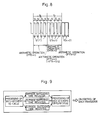
- Fig.1 and Fig.2 shown a pulse width modulation (hereinafter abbreviated as PWM) control unit.
- reference numeral 1 designates an induction motor having three-phase widing 2 with three windings 2a, 2b, 2c Y-connected.
- Reference numeral 3 designates a voltage type inverter connected to the induction motor 1. The inverter 3 is provided with a transistor bridge circuit 4 connected to the three-phase winding 2 of the induction motor 1.
- the bridge circuit 4 has plural (six) transistors, such as MOSFET, (switching elements) (Tra), (Tra'), (Trb), (Trb'), (Trc), (Trc'), each having a reflux diode (Da) - (Dc').
- DC voltage is applied to the inverter 3 from a rectifier 6 which rectifies three-phase AC of three-phase power source 5.
- Reference numeral 8 designates a one-chip microcomputer which forms ON time (namely, PWM control pattern) of six transistors (Tra) - (Trc') of the bridge circuit 4.
- the microcomputer 8 is provided with a base driver 8a which ON/OFF operates the transistors (Tra) - (Trc').
- DC is pulse-width modulated.
- formation of PWM control pattern is made by determining the PWM control pattern so as to make a locus of time integral of output voltage resemble a circular locus.
- va, vb, vc are voltage of output terminal of the inverter 3 and vn is voltage of neutral point of the three-phase winding 2 and also output voltage vector v and time integral ⁇ p of the voltege vector v p which are defined by the following formulae are taken into. consideration.
- V 1 Effective voltage of fundamental wave
- On/OFF pattern (PWM control pattern) of each transistor (Tra) - (Trc') is obtained.
- PWM control patterns are represented by four patterns shown by Figs.5(a)-(d) (in the figure, ⁇ + and ⁇ - show respectively ON time of the transistor on (+) side and ON time of the transistor on (-) side.
- the PWM control pattern is determined necessarily if only the mane of a transistor which performs first the ON motion in the period To and the time when the transistor turns to OFF motion, the PWM control pattern can be determined by the following formulae, with reference to the above (3) formulae and Fig.5(a)-(d), provided that the angle ⁇ is within the range of O ⁇ /3.
- the relative formulae (4) of the PWM control pattern within the above range of 0 ⁇ /3 can be relative formulae if each symbol is permutated as shown in the following Table II in the same way as stated before. If ON time of each switching element is calculated on the basis of calculation formulae of the above (4) or (5) relative formulae, not only calculating time can be reduced comparatively but also either of two transistors can always be ON controlled and PWM control patterns can be calculated only by two sets of times (saving of one set of timers). How to use properly the above (4) and (5) relative formulae is indicated below.
- the permutation table in the above Table II is stored beforehand in the microcomputer 8.
- the flow chart of Fig.6 is for calculating ON time (PWM control pattern) of each transistor (Tra) - (Trc') and the flow chart of Fig.7 is for controlling actually each transistor (Tra) - (Trc').
- ON time ⁇ (n+1) of each transistor (Tra) - (Trc') is calculated on the basis of the relative formulae (4) of PWM control pattern and the permutation table of Table II at the step S A2 .
- the divided pulse ⁇ '(n+1) is stored in a switching time register for each phase (in the voltage type inerter, since either of two transistors is always in ON state in the arms of each phase, one registor is enough for each phase), and "RETURN".
- an arithmetic operation means 10 by which at the step S A1 and the step S A2 On time ⁇ '(n+1) of each transistor (switching element) (Tra) - (Trc') is calculated at the calculation period according to the carrier frequency (5KHz) and on the basis of the above relative formulae (4) of the PWM control pattern and transistors (Tra) ⁇ (Trc') which should take the calculated ON time ⁇ (n+1) are specified on the basis of the permutation table of Table II.
- ON time ⁇ (n+1) of each transistor (Tra) - (Trc') is calculated by the program of the flow chart for calculating PWM control patterns (Fig.6) and on the basis of the relative formulae (4) of PWM control pattern and transistors (Tra) - (Trc') which should be ON controlled by the ON time are specified by the arithmetic operation means 10 and on the basis of the permutation table of Table II.
- That part of the contents of a switching time register of each phase which is converted to pulse-width can be processed by hardware, such as IC for pulse-width modulation connected from the outside.
- hardware such as IC for pulse-width modulation connected from the outside.
- IC for pulse-width modulation
- step S B2 The common use of the switching time register and a register of pulse-width controlling part (step S B2 ) will dispense with the process of the step S B1 in Fig.7.
- the calculation period To of the calculation flow of PWM control pattern is determined necessarily by the time required for calculating PWM control pattern actually, but the period To' of ON control of transistors in the flow chart of Fig.7 is determined according to the desired carrier frequency, for which the value of the number of divisions N(To/To') of ON time of each transistor should be set properly.
- the division into pulses of unequal width is carried out by linear-interpolating between ON time ⁇ (n) of transistor in the period To and ON time ⁇ (n+1) in the succeeding period To.
- phase ⁇ t and amplitude V 1 of output voltage are inputted and at the step Sc 2 calculated result of ON time ⁇ '(n-1) (pulse divided into four) of each transistor Tra-(Trc') is inputted.
- ON Time ⁇ (n) of each transistor (Tra) - (Trc') of this time is calculated on the basis of the relative formulae (4) of PWM control pattern and this ON time is divided into the plural number N(4) to obtain divided pulses ⁇ '(n) and then, at the step S c4 , according to the difference between the last time and this time, the interpolation value ⁇ n+1 of the divided pulse ⁇ '(n-1) of the last time is calculated on the basis of the following formula.
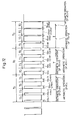
- the flow chart of Fig.11 is for ON controlling each transistor (Tra) - (Trc') with the divided pulse ⁇ ' for the duration from period To to the third period To in which divided pulse ⁇ ' was calculated and stored as shown in Fig. 12.
- the third and the fourth switching time registers in order is read in for ON controlling each transistor (Tra)-(Trc').
- the division of ON time by the dividing means 11 is carried out for pulse of unequal width as shown by Fig.12 and if the divided pulse ⁇ ' is outputted at the first period T'o, at the next period T' 0 the divided pulse which is larger than the above divided pulse by the interpolated value ⁇ is outputted and this is repeated at every period T'o of control. Therefore, as compared with the case where division of ON time is carried out for pulse of equal width (the case shown by Fig.15(a)), as shown in Fig.14 and Fig.15(b) wave form can be repreduced precisely to the mean value v of output voltage at the control period T'o corresponding to the equivalent carrier frequency. Also, in the case where ON Time is divided into pulses of unequal width by linear interpolation, precessing time of the microcomputer 8 required for division is comparatively short and equivalent carrier frequency can be raised fully.
- Fig.16 and Fig.17 show the second modified example which carries out the division into pulses of unequal width on the basis of the correction value table stored beforehand.
- each of three pulses of unequal width which lies intermediate has an error ⁇ 1 , ⁇ ⁇ 2 , D ⁇ 3 respectively in relation to the real value of signal wave (sin ⁇ t). Since each error ⁇ i is determined necessarily if only the shape of a since wave function (determined by amplitude Vi and phase ⁇ t) and the period To of calculating ON time are determined, a correction value table which stores beforehand the error ⁇ i according to amplitude V 1 , phase ⁇ t and calculating period To of ON time is prepared and this correction value table is stored in the microcomputer 8.
- Fig.16 is a block composition diagram of the microcomputer 8 in the case where division into pulses of unequal width is carried out on the basis of the correction value table.
- reference numeral 15 designates an ON time operation circuit which inputs amplitude V 1 and phase ⁇ t of output voltage and calculation period To of ON time and calculation ON time of each transistor (Tra) - (Trc') on the basis of the flow chart of Fig.6.
- Reference numeral 17 designates a correction value reading out circuit which inputs amplitude Vi and phase ⁇ t of the output voltage and the calculation period To of ON time and reads out correction values ⁇ i corresponding to them from the correction value table.
- Each transistor (Tra) - (Trc') is ON controlled by the pulse of unequal width corrected by the pulse of unequal width correcting circuit 18.
- each of three (N-1) intermediate pulses of unequal width can be reproduced precisely in wave form by the corresponding correction value ⁇ i.
- the correction value table can store correction coefficient in lieu of the correction data.
- correction is made by multiplying the quantity of change ⁇ of pulse of unequal width by a correction coeffiecient, as indicated by the following formulae.
- division into pulses of unequal width by the dividing means 11 is carried out on the basis of linear interpolation and the corrected value table but it is a matter of course that the other interpolating method of higher order is applicable to the division into plural pulses of unequal width.
- the third modified example is shown in Fig.18.
- Fig.18 it is selected properly according to the rate of change of ON time whether division of ON time of each transistor (Tra) - (Trc') should be carried out for pulses of equal width or pulses of unequal width.
- ON time ⁇ a of transistor is within the range of Sin( ⁇ 0 + ⁇ /3) as shown in Fig.19 and the rate of change of the ON time is small. Therefore, division into pulses of equal width in a short calculation time is carried out so as to reproduce wave form precisely.
- the ON time T b of transistor is within the range of Sin(po and its rate of change of ON time is large, division into pulses of unequal width is adopted so as to reproduce wave form precisly.
- ON time of transistor is divided into pulses of equal width or pulses of unequal width on the basis of the rate of change of the ON time within the whole range of 0 ⁇ 0 ⁇ 2 ⁇ of angle ⁇ 0 .
- reference numeral 15 designates a sectional information calculation circuit which discriminates the section N in Table II from the phase wt.
- ⁇ 0 ⁇ t-(N ⁇ /3)
- Reference numeral 17 designates a pulse dividing circuit which inputs the angel ⁇ 0 and the effective value V i of voltage of fundamental wave, calculates ON time of each transistor (Tra) - (Trc') on the basis of the relative formulae (4) of PWM control pattern, similarly to the flow chart of Fig.6, and divides the ON time into plural pulses of equal width.
- Reference numeral 18 designates a pulse of unequal width calculation circuit which receives ON time of each transistor (Tra) - (Trc') calculated by the pulses dividing circuit 17, divided pulses of equal width and sectional signals N from the section information calculating circuit 15, grasps ON time (function of SinO - Sin ⁇ /3 in Tablell) of transistors (Tra) - (Trc') to be divided into pulses of unequal width on the basis of the Table II according to the section N, divides only ON time which should be divided into pulses of unequal width into plural pulses of unequal width by the linear interpolation based on the motion similar to the flow chart of Fig.10 and Fig.11 or by the interplation table of the second modified example and outputs the divided pulses of unequal width and pulses of equal width equally divided by the pulse dividing circuit 17 to the base driver 18a.
- division of ON time by the dividing means 11 is carried out for puses of unequal width when the rate of change of ON time is large as shown by Fig.19 and therefore as compared with the case where division is carried out for pulses of equal width (the case shown by Fig.15(a)), wave form can be reproduced precisely in relation to the mean value v of output voltage in the control period T'o corresponding to the equivalent carrier frequency as shown in Fig.19.
- calculation of PWM control pattern can be carried out equally throughout the whole range of angle ⁇ t by utilizing the objectivity of voltage vector and thereafter, it can be easily grasped whether ON time should be divided into pulses of equal width or into pulses of unequal width on the basis of Table II.
- this process is suitabl for a microcomputer and more simplification of process is made possible.
- the one-chip microcomputer 8 which forms the PWM control pattern contains the ON time arithmetic operation circuit 10 as an arithmetic operation means which calculates in the same way as the flow chart of Fig.6, the dividing circuit 11 as a dividing means which divides ON time if each transistor (Tra) - (Trc') calculated by the ON time arithmetic operation circuit 10 into plural pulses and a pulse-width controlling circuit 12 as a controlling means which ON controls each transistor (Tra) - (Trc') by driving the base driver 8a with pulses divided by the dividing circuit 11.
- the ON time arithmetic operation circuit 10 as an arithmetic operation means which calculates in the same way as the flow chart of Fig.6
- the dividing circuit 11 as a dividing means which divides ON time if each transistor (Tra) - (Trc') calculated by the ON time arithmetic operation circuit 10 into plural pulses
- a pulse-width controlling circuit 12 as a controlling means which ON controls
- Reference numeral 13 designates a ripple detecting circuit which detects ripple of torque generated by the induction motor 1.
- Reference numeral 14 is incorporated in the microcomputer 8 and is a number of divisions setting circuit having a number of divisions table in which the value of number of divisions N of ON time of the dividing circuit 11 is stored according to the value of ripple of torque generated by the induction motor 1.
- the number of divisions N of the number of divisions setting circuit 14 is so set that it becomes larger by stages as the ripple of torque becomes larger and is stored.
- the value of number of divisions N according to the size of the ripple of torque detected by the ripple detecting circuit 13 is read out by number of divisions setting circuit 14 and the value of this number of divisions N is outputted to the dividing circuit 11 for the division of ON time.
- the ripple of torque generated by the induction motor 1 becomes larger in electrical angle at every ⁇ /3 as shown by Fig.21.
- This ripple is detected by the torque ripple detecting circuit 13 and the number of divisions N corresponding to the size of this ripple is set by the number of divisions setting circuit 14. Therefore, in the state where torque ripple is large, number of divisions is set at a large value and ON time is divided in more numbers than usual in the state where torque ripple is large, with the result that carrier frequency is raised equivalently to the full. Consequently, ripple of torque of the induction motor 1 is restricted effectively and the induction motor 1 is driven to turn by uniformalized torque.
- ripple of torque is periodic according to the change of phase ⁇ t and therefore as shown in Fig.22, provision of the number of divisions setting circuit 14' having a number of divisions table which stores beforehand the number of divisions N corresponding to phase ⁇ t can dispense with the torque ripple detecting circuit 13.
- Fig.22 shows the fifth modified example.
- the value of number of divisions N for dividing ON time of each transistor (Tra) - (Trc') is changed according to the ripple of torque of the induction motor 1 but in this modified example, in the case where the ripple of current flowing through the three-phase winding 2 and the ripple of voltage are restricted, number of divisions N is set variable according to phase ⁇ t of signal wave, namely, according to the rate of change of ON time of each transistor (Tra) - (Trc').
- the number of division table is stored beforehand in the number of divisions setting circuit 14'.
- the value of Number of divisions N is stored within the range of 0 ⁇ 0 ⁇ 2 ⁇ of angle ⁇ 0 , with reference to Table II.
- ON time of each transistor (Tra) - (Trc') calculated by the arithmetic operation means 10' is divided by the number of divisions N which is so set that the larger the rate of change of the ON time ⁇ , the larger the value, as shown by Fig.23 and Fig.24 (Fig.23 is the case of division into pluses of unequal width and Fig.24 is the case of division into pulses of equal width) and therefore, ripple of current and ripple of voltage can be restricted effectively.
- Fig.25 shows the sixth modified example.
- ON time of each transistor (Tra) - (Trc') is divided by the number of divisions N which is set variable according to the rate of change of ON time, proper choice is given between division into pulses of equal width and division into pulses of unequal width according to the rate of change.
- Fig.25 among the range of phase of signal wave shown by broken lines, in the range where the rate of change of ON time is large, the division of ON time is carried out for pulses of unequal width and in the range where phase of signal wave is small the division of ON time is carried out for pulses of equal width.
- Setting of the number of division N is the same as in the case of the fifth modefied example.
- FIG.26 A flow chart for preventing the short-circuit is shown in Fig.26.
- step S E1 after start ON time of each transistor (Tra) - (Trc') is calculated and at the step S E2 the value of number of divisions N is read out and ON time of each transistor (Tra) - (Trc') is divided into the plural number N by this number of divisions N.
- the width T of the divided pulse is compared with the arm short-circuit preventive time Td and in the case of T ⁇ Td, output pulse is concluded to vanish and at the step SE4, the number of divisions N is reduced and returned to the step S E2 , where ON time of each transistor (Tra) - (Trc') is divided by the reduced number of divisions N.
Landscapes
- Engineering & Computer Science (AREA)
- Power Engineering (AREA)
- Inverter Devices (AREA)
Applications Claiming Priority (10)
| Application Number | Priority Date | Filing Date | Title |
|---|---|---|---|
| JP95200/88 | 1988-04-18 | ||
| JP63095200A JP2705093B2 (ja) | 1988-04-18 | 1988-04-18 | インバータのパルス幅変調制御装置 |
| JP127948/88 | 1988-05-25 | ||
| JP63127948A JPH0832183B2 (ja) | 1988-05-25 | 1988-05-25 | インバータのパルス幅変調制御装置 |
| JP63132460A JP2569724B2 (ja) | 1988-05-30 | 1988-05-30 | インバータのパルス幅変調制御装置 |
| JP63132461A JPH07114548B2 (ja) | 1988-05-30 | 1988-05-30 | インバータのパルス幅変調制御装置 |
| JP63132459A JPH0744843B2 (ja) | 1988-05-30 | 1988-05-30 | インバータのパルス幅変調制御装置 |
| JP132461/88 | 1988-05-30 | ||
| JP132459/88 | 1988-05-30 | ||
| JP132460/88 | 1988-05-30 |
Publications (3)
| Publication Number | Publication Date |
|---|---|
| EP0338798A2 true EP0338798A2 (de) | 1989-10-25 |
| EP0338798A3 EP0338798A3 (en) | 1990-07-04 |
| EP0338798B1 EP0338798B1 (de) | 1994-07-13 |
Family
ID=27525728
Family Applications (1)
| Application Number | Title | Priority Date | Filing Date |
|---|---|---|---|
| EP89303871A Expired - Lifetime EP0338798B1 (de) | 1988-04-18 | 1989-04-18 | Pulsbreitenmodulierungssteuereinheit für Wechselrichter |
Country Status (5)
| Country | Link |
|---|---|
| US (1) | US4989128A (de) |
| EP (1) | EP0338798B1 (de) |
| AU (1) | AU621868B2 (de) |
| DE (1) | DE68916684T2 (de) |
| ES (1) | ES2056213T3 (de) |
Cited By (2)
| Publication number | Priority date | Publication date | Assignee | Title |
|---|---|---|---|---|
| EP0467694A3 (en) * | 1990-07-20 | 1992-04-22 | Kabushiki Kaisha Toshiba | Three-phase pwm signal generating device for inverters |
| EP0655835A1 (de) * | 1993-11-30 | 1995-05-31 | Robert Bosch Gmbh | Verfahren und Vorrichtung zur Steuerung elektrischer Geräte mittels einer Pulsweitenmodulation-Einrichtung |
Families Citing this family (9)
| Publication number | Priority date | Publication date | Assignee | Title |
|---|---|---|---|---|
| US5372138A (en) | 1988-03-21 | 1994-12-13 | Boston Scientific Corporation | Acousting imaging catheters and the like |
| US5383107A (en) * | 1992-11-06 | 1995-01-17 | Sundstrand Corporation | Harmonic control for an inverter by use of an objective function |
| US5844397A (en) * | 1994-04-29 | 1998-12-01 | Reda Pump | Downhole pumping system with variable speed pulse width modulated inverter coupled to electrical motor via non-gap transformer |
| FI110372B (fi) * | 1999-02-15 | 2002-12-31 | Abb Industry Oy | Menetelmä sähkökoneen ohjaamiseksi ja vaihtosuuntaaja |
| KR100325407B1 (ko) * | 1999-07-09 | 2002-03-04 | 이종수 | 펄스폭 변조 제어 시스템 |
| GB201223174D0 (en) * | 2012-12-21 | 2013-02-06 | Trw Ltd | Control of electric motors |
| US9007140B1 (en) | 2013-01-08 | 2015-04-14 | University Of South Florida | Digitally controlled wide range pulse width modulator |
| JP6729795B2 (ja) * | 2017-03-29 | 2020-07-22 | アイシン・エィ・ダブリュ株式会社 | 回転電機制御装置 |
| CN113037072B (zh) * | 2021-05-28 | 2021-08-17 | 天津飞旋科技股份有限公司 | 一种窄脉冲抑制方法、装置和桥式开关电路 |
Family Cites Families (9)
| Publication number | Priority date | Publication date | Assignee | Title |
|---|---|---|---|---|
| US4322786A (en) * | 1980-08-04 | 1982-03-30 | Coulter Systems Corp. | Pulse burst regulated d.c. power supply apparatus and method |
| JPS605782A (ja) * | 1983-06-22 | 1985-01-12 | Hitachi Ltd | インバ−タ装置 |
| DE3486449T2 (de) * | 1983-11-28 | 1997-11-27 | Matsushita Electric Ind Co Ltd | Pulsbreitenmodulationswechselrichtervorrichtung |
| JPS61224874A (ja) * | 1985-03-29 | 1986-10-06 | Toshiba Electric Equip Corp | インバ−タ装置 |
| US4713220A (en) * | 1985-04-22 | 1987-12-15 | National Distillers And Chemical Corporation | Ozonator power supply |
| JPS62118774A (ja) * | 1985-11-18 | 1987-05-30 | Toshiba Corp | インバ−タのパルス幅変調信号発生方式 |
| JPH0697854B2 (ja) * | 1986-01-11 | 1994-11-30 | 株式会社日立製作所 | 電力変換装置の制御装置 |
| GB2186127B (en) * | 1986-01-11 | 1990-03-21 | Hitachi Ltd | Apparatus for controlling power transducers |
| JPS62163589A (ja) * | 1986-01-13 | 1987-07-20 | Hitachi Ltd | パルス幅変調インバ−タによる誘導電動機の制御装置 |
-
1989
- 1989-04-17 AU AU33084/89A patent/AU621868B2/en not_active Ceased
- 1989-04-18 ES ES89303871T patent/ES2056213T3/es not_active Expired - Lifetime
- 1989-04-18 EP EP89303871A patent/EP0338798B1/de not_active Expired - Lifetime
- 1989-04-18 DE DE68916684T patent/DE68916684T2/de not_active Expired - Fee Related
- 1989-04-18 US US07/340,023 patent/US4989128A/en not_active Expired - Fee Related
Cited By (3)
| Publication number | Priority date | Publication date | Assignee | Title |
|---|---|---|---|---|
| EP0467694A3 (en) * | 1990-07-20 | 1992-04-22 | Kabushiki Kaisha Toshiba | Three-phase pwm signal generating device for inverters |
| US5182701A (en) * | 1990-07-20 | 1993-01-26 | Kabushiki Kaisha Toshiba | Three-phase pwm inverter providing an improved output sinusoidal waveform |
| EP0655835A1 (de) * | 1993-11-30 | 1995-05-31 | Robert Bosch Gmbh | Verfahren und Vorrichtung zur Steuerung elektrischer Geräte mittels einer Pulsweitenmodulation-Einrichtung |
Also Published As
| Publication number | Publication date |
|---|---|
| EP0338798B1 (de) | 1994-07-13 |
| AU621868B2 (en) | 1992-03-26 |
| EP0338798A3 (en) | 1990-07-04 |
| DE68916684D1 (de) | 1994-08-18 |
| DE68916684T2 (de) | 1994-10-27 |
| ES2056213T3 (es) | 1994-10-01 |
| US4989128A (en) | 1991-01-29 |
| AU3308489A (en) | 1989-10-19 |
Similar Documents
| Publication | Publication Date | Title |
|---|---|---|
| US4617675A (en) | Digital PWMed pulse generator | |
| EP0351783B1 (de) | Pulsbreitenmodulierte Wechselrichter-Einrichtung | |
| EP0338798B1 (de) | Pulsbreitenmodulierungssteuereinheit für Wechselrichter | |
| EP0593738A1 (de) | Programmierter pbm-umrichterregler | |
| JP4187831B2 (ja) | デジタルデータをフルブリッジ出力段部駆動用のpwm信号に変換するときの精細度を増加させる装置及び方法 | |
| JPS62163589A (ja) | パルス幅変調インバ−タによる誘導電動機の制御装置 | |
| JP6987304B2 (ja) | 電力変換装置、機械学習器、および学習済みモデルの生成方法 | |
| JP2000505638A (ja) | 直接トルク制御インバータ装置 | |
| US4477763A (en) | Method of controlling inverter and system therefor | |
| CN100438314C (zh) | 驱动步进电机的电路以及控制步进电机驱动器的方法 | |
| US12283899B2 (en) | Power conversion device | |
| US6459601B1 (en) | Control circuit of power converter | |
| Grabowski | Direct torque neuro-fuzzy control of induction motor drive | |
| JP2703711B2 (ja) | Pwmインバータの制御方法 | |
| JPH06245588A (ja) | Pwmインバータ制御方法 | |
| JP2569724B2 (ja) | インバータのパルス幅変調制御装置 | |
| JPH04222466A (ja) | インバータのパルス幅変調制御方法およびその装置 | |
| KR920002587B1 (ko) | 공진형 인버터의 최적출력전류제어시스템 | |
| JPH01303093A (ja) | インバータのパルス幅変調制御装置 | |
| JPH0744843B2 (ja) | インバータのパルス幅変調制御装置 | |
| JP7734099B2 (ja) | モータ駆動制御装置、モータユニット、およびモータ駆動制御方法 | |
| US20260019007A1 (en) | Model predictive control for converter with filter cells based on offline-computed pulse patterns and online cell balancing | |
| JP3381862B2 (ja) | インバータのパルス幅変調方法およびその装置 | |
| SU1767665A1 (ru) | Способ управлени инвертором на полностью управл емых вентил х с широтно-импульсной модул цией | |
| JPH08205586A (ja) | 同期電動機の制御装置 |
Legal Events
| Date | Code | Title | Description |
|---|---|---|---|
| PUAI | Public reference made under article 153(3) epc to a published international application that has entered the european phase |
Free format text: ORIGINAL CODE: 0009012 |
|
| AK | Designated contracting states |
Kind code of ref document: A2 Designated state(s): BE DE ES FR GB GR IT |
|
| PUAL | Search report despatched |
Free format text: ORIGINAL CODE: 0009013 |
|
| AK | Designated contracting states |
Kind code of ref document: A3 Designated state(s): BE DE ES FR GB GR IT |
|
| 17P | Request for examination filed |
Effective date: 19901203 |
|
| 17Q | First examination report despatched |
Effective date: 19930121 |
|
| GRAA | (expected) grant |
Free format text: ORIGINAL CODE: 0009210 |
|
| ITF | It: translation for a ep patent filed | ||
| AK | Designated contracting states |
Kind code of ref document: B1 Designated state(s): BE DE ES FR GB GR IT |
|
| REF | Corresponds to: |
Ref document number: 68916684 Country of ref document: DE Date of ref document: 19940818 |
|
| ET | Fr: translation filed | ||
| REG | Reference to a national code |
Ref country code: ES Ref legal event code: FG2A Ref document number: 2056213 Country of ref document: ES Kind code of ref document: T3 |
|
| REG | Reference to a national code |
Ref country code: GR Ref legal event code: FG4A Free format text: 3013518 |
|
| PLBE | No opposition filed within time limit |
Free format text: ORIGINAL CODE: 0009261 |
|
| STAA | Information on the status of an ep patent application or granted ep patent |
Free format text: STATUS: NO OPPOSITION FILED WITHIN TIME LIMIT |
|
| 26N | No opposition filed | ||
| PGFP | Annual fee paid to national office [announced via postgrant information from national office to epo] |
Ref country code: GB Payment date: 19980409 Year of fee payment: 10 Ref country code: FR Payment date: 19980409 Year of fee payment: 10 |
|
| PGFP | Annual fee paid to national office [announced via postgrant information from national office to epo] |
Ref country code: DE Payment date: 19980424 Year of fee payment: 10 |
|
| PGFP | Annual fee paid to national office [announced via postgrant information from national office to epo] |
Ref country code: ES Payment date: 19980428 Year of fee payment: 10 |
|
| PGFP | Annual fee paid to national office [announced via postgrant information from national office to epo] |
Ref country code: GR Payment date: 19980430 Year of fee payment: 10 |
|
| PGFP | Annual fee paid to national office [announced via postgrant information from national office to epo] |
Ref country code: BE Payment date: 19980609 Year of fee payment: 10 |
|
| PG25 | Lapsed in a contracting state [announced via postgrant information from national office to epo] |
Ref country code: GB Free format text: LAPSE BECAUSE OF NON-PAYMENT OF DUE FEES Effective date: 19990418 |
|
| PG25 | Lapsed in a contracting state [announced via postgrant information from national office to epo] |
Ref country code: ES Free format text: LAPSE BECAUSE OF NON-PAYMENT OF DUE FEES Effective date: 19990419 |
|
| PG25 | Lapsed in a contracting state [announced via postgrant information from national office to epo] |
Ref country code: GR Free format text: LAPSE BECAUSE OF NON-PAYMENT OF DUE FEES Effective date: 19990430 Ref country code: BE Free format text: LAPSE BECAUSE OF NON-PAYMENT OF DUE FEES Effective date: 19990430 |
|
| BERE | Be: lapsed |
Owner name: DAIKIN INDUSTRIES LTD Effective date: 19990430 |
|
| GBPC | Gb: european patent ceased through non-payment of renewal fee |
Effective date: 19990418 |
|
| PG25 | Lapsed in a contracting state [announced via postgrant information from national office to epo] |
Ref country code: FR Free format text: LAPSE BECAUSE OF NON-PAYMENT OF DUE FEES Effective date: 19991231 |
|
| REG | Reference to a national code |
Ref country code: FR Ref legal event code: ST |
|
| PG25 | Lapsed in a contracting state [announced via postgrant information from national office to epo] |
Ref country code: DE Free format text: LAPSE BECAUSE OF NON-PAYMENT OF DUE FEES Effective date: 20000201 |
|
| REG | Reference to a national code |
Ref country code: ES Ref legal event code: FD2A Effective date: 20010503 |
|
| PG25 | Lapsed in a contracting state [announced via postgrant information from national office to epo] |
Ref country code: IT Free format text: LAPSE BECAUSE OF NON-PAYMENT OF DUE FEES;WARNING: LAPSES OF ITALIAN PATENTS WITH EFFECTIVE DATE BEFORE 2007 MAY HAVE OCCURRED AT ANY TIME BEFORE 2007. THE CORRECT EFFECTIVE DATE MAY BE DIFFERENT FROM THE ONE RECORDED. Effective date: 20050418 |