EP0337659B1 - Lötstift-Rückhaltevorrichtung - Google Patents
Lötstift-Rückhaltevorrichtung Download PDFInfo
- Publication number
- EP0337659B1 EP0337659B1 EP89303387A EP89303387A EP0337659B1 EP 0337659 B1 EP0337659 B1 EP 0337659B1 EP 89303387 A EP89303387 A EP 89303387A EP 89303387 A EP89303387 A EP 89303387A EP 0337659 B1 EP0337659 B1 EP 0337659B1
- Authority
- EP
- European Patent Office
- Prior art keywords
- mounting portion
- spacer plate
- solder
- assembly
- channels
- Prior art date
- Legal status (The legal status is an assumption and is not a legal conclusion. Google has not performed a legal analysis and makes no representation as to the accuracy of the status listed.)
- Expired - Lifetime
Links
Images

Classifications
-
- H—ELECTRICITY
- H01—ELECTRIC ELEMENTS
- H01R—ELECTRICALLY-CONDUCTIVE CONNECTIONS; STRUCTURAL ASSOCIATIONS OF A PLURALITY OF MUTUALLY-INSULATED ELECTRICAL CONNECTING ELEMENTS; COUPLING DEVICES; CURRENT COLLECTORS
- H01R4/00—Electrically-conductive connections between two or more conductive members in direct contact, i.e. touching one another; Means for effecting or maintaining such contact; Electrically-conductive connections having two or more spaced connecting locations for conductors and using contact members penetrating insulation
- H01R4/02—Soldered or welded connections
-
- H—ELECTRICITY
- H01—ELECTRIC ELEMENTS
- H01R—ELECTRICALLY-CONDUCTIVE CONNECTIONS; STRUCTURAL ASSOCIATIONS OF A PLURALITY OF MUTUALLY-INSULATED ELECTRICAL CONNECTING ELEMENTS; COUPLING DEVICES; CURRENT COLLECTORS
- H01R12/00—Structural associations of a plurality of mutually-insulated electrical connecting elements, specially adapted for printed circuits, e.g. printed circuit boards [PCB], flat or ribbon cables, or like generally planar structures, e.g. terminal strips, terminal blocks; Coupling devices specially adapted for printed circuits, flat or ribbon cables, or like generally planar structures; Terminals specially adapted for contact with, or insertion into, printed circuits, flat or ribbon cables, or like generally planar structures
- H01R12/70—Coupling devices
- H01R12/71—Coupling devices for rigid printing circuits or like structures
- H01R12/712—Coupling devices for rigid printing circuits or like structures co-operating with the surface of the printed circuit or with a coupling device exclusively provided on the surface of the printed circuit
-
- H—ELECTRICITY
- H01—ELECTRIC ELEMENTS
- H01R—ELECTRICALLY-CONDUCTIVE CONNECTIONS; STRUCTURAL ASSOCIATIONS OF A PLURALITY OF MUTUALLY-INSULATED ELECTRICAL CONNECTING ELEMENTS; COUPLING DEVICES; CURRENT COLLECTORS
- H01R12/00—Structural associations of a plurality of mutually-insulated electrical connecting elements, specially adapted for printed circuits, e.g. printed circuit boards [PCB], flat or ribbon cables, or like generally planar structures, e.g. terminal strips, terminal blocks; Coupling devices specially adapted for printed circuits, flat or ribbon cables, or like generally planar structures; Terminals specially adapted for contact with, or insertion into, printed circuits, flat or ribbon cables, or like generally planar structures
- H01R12/50—Fixed connections
- H01R12/51—Fixed connections for rigid printed circuits or like structures
- H01R12/55—Fixed connections for rigid printed circuits or like structures characterised by the terminals
- H01R12/58—Fixed connections for rigid printed circuits or like structures characterised by the terminals terminals for insertion into holes
-
- H—ELECTRICITY
- H05—ELECTRIC TECHNIQUES NOT OTHERWISE PROVIDED FOR
- H05K—PRINTED CIRCUITS; CASINGS OR CONSTRUCTIONAL DETAILS OF ELECTRIC APPARATUS; MANUFACTURE OF ASSEMBLAGES OF ELECTRICAL COMPONENTS
- H05K3/00—Apparatus or processes for manufacturing printed circuits
- H05K3/30—Assembling printed circuits with electric components, e.g. with resistors
- H05K3/306—Assembling printed circuits with electric components, e.g. with resistors with lead-in-hole components
- H05K3/308—Adaptations of leads
Definitions
- the present invention relates to electrical connectors and in particular to a solder post retention system for preventing axial movement of solder posts once assembled into right angle mounted connectors.
- Maintaining the position of solder posts in connectors has been recognized as desirable for some time and permits predrilling of the array of holes in the printed circuit board knowing that the solder posts of a connector will correspond in position. Most attention has been given to maintaining the horizontal position of the solder posts.
- the present invention consists in a right angle electrical connector assembly as defined in claim 1.
- DE-A-33 30 151 discloses an electrical connector assembly in which a secondary locking plate engages in a slot in an insulating housing having cavities containing electrical terminals.
- the locking plate has channels each receiving a circular cross section mating portion of an electrical terminal so that the edges of each channel engage in a peripheral groove in the respective mating portion.
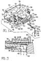
- FIG. 1 there is depicted therein a perspective view of an electrical connector assembly 20 in accordance with an embodiment of the present invention.
- the connector assembly 20 shown is exemplary and is one of a well known type, namely a subminiature D connector of the type manufactured by the assignee, AMP Incorporated, and sold under the trademark AMPLIMITE.
- Connector 20 comprises housing 22 molded of thermoplastic with integral peripheral flange 24, mating face 26, opposed rear face 28 and mounting face 30 at a right angle with respect to mating face 26.
- Cavity 32 is recessed from rear face 28 and defines recessed face 34.
- a plurality of contact receiving passages 36 extend from mating face 26 rearward toward rear face 28, open to recessed face 34 and have contacts 38 secured therein.
- Recessed face 34 is not limited to being planar but could, for example, be stepped.
- Contacts 38 have a mating portion 40 extending into contact receiving passages 36 that may be either pins or sockets, and extend into cavity 32 with mounting portions 42, typically solder posts 44, that extend through post spacer plate 46.
- housing 22 is molded in a single piece with post spacer plate 46 integral therewith. Housing 22 also has apertures 48 for removal of vapor phase material. Mating face 26 is surrounded by flange 24 having mounting apertures 50 at opposite ends thereof for securing a complementary connector (not shown) thereto.
- Electrically conductive shell 52 has a similar outer profile to flange 24 with shell mounting apertures 54 aligned with apertures 50. Lugs 56 on the upper portion of shell 52 fold into recesses 58 on flange 24 to secure shell 52 to housing 22. Shroud 60 extends upward from the flat portion of shell 52 and conforms to and encloses the forward raised portion 62 of housing 22.
- Mounting face 30 of connector assembly 20 has integral flanges 64 at opposite ends thereof.
- Each flange 64 has a coplanar mounting face 30 which is received against a printed circuit board (not shown) with channels 66 provided for flux removal, an opposed holding face 68 with aperture 70 extending therebetween.
- Shell 52 has integral ground straps 72 extending to respective mounting faces 30.
- Ground straps 72 fold into channel 74, such that the lower surface of ground strap is coplanar with mounting face 30, and widens near rear face 28 forming shoulders 76 that engage stops 78 to aid in securing ground strap 72 to housing 22 during unmating of a complementary connector.
- Apertures 80 in the widened region of ground strap 72 align with apertures 70 in flange 64.
- Contacts 38 are formed in a strip on the desired centerline spacing such as in accordance with the teaching of United States Patent No. 4, 775,336, said application being hereby incorporated by reference.
- contacts 38 on a common carrier strip 82 are unwound from a reel (not shown).
- a length of carrier strip 82 called a "comb" having the number of contacts 38 confirming to the number of contact receiving passages 36 in a row of housing 22 is severed from the reel.
- the solder posts 44 of the contacts 38 on the comb of severed carrier strip 82 are formed to be substantially perpendicular to the mating portion 40 of contacts 38.
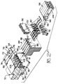
- Loading block 84 is inserted into cavity 32 seating on recessed face 34.
- Loading block 84 has a plurality of channels 86 aligned with and corresponding in number to contact receiving passages 36 in the row of passages 36 into which contacts 38 will be inserted. Channels 86 thus provide an extension of contact receiving cavity 36 toward or beyond rear face 28. Channels 86 in loading block 84 open to surface 88 of block 84 through slots 91.
- the row of contact receiving passages 36 closest to post spacer plate 46 is typically the first to receive contacts 38, then the next closets row of contact receiving passages 36 and so on.
- a different loading block 84 is used for each row of passages 36 with channels 86 therein aligned with passages 36 in the row of passages into which the contacts 38 are being inserted.
- Contacts 38, bent 90 degrees and still integral with carrier strip 82 are partially inserted into respective channels 86 in loading block 84.
- Contacts 36 are loose pieced by shearing carrier strip 82 between punch 90 and anvil 92 then inserted to a predetermined depth in passages 36 by passing through respective channels 86 in loading block 84 thence into passages 36.
- Insertion tool 94 provides the insertion force to insert contacts 38 into housing 22.
- mating portion push surface 96 engages the rear surface of mating portion 40
- insertion feature push surface 98 engages insertion feature 100
- solder post push feature 102 engages substantially the length of solder post 44.
- barbs 95 for securing contact 38 in contact receiving passage 38 in an interference fit pass through side channels 87 and solder posts 44 extend through slots 91 and post spacer plate 46. At least a portion 104 of insertion tool 94 passes through slot 91 and channels 106 in post spacer plate 46.
- Channels 106 may have detents 93 therealong in which solder tails 44 are secured.
- the detents 93 form a row or rows along spacer plate 46 with the number of detents 93 in a given channel 106 corresponding to the number of contact receiving passages 36 laterally aligned with that channel.
- Figure 1 includes a perspective view of a typical socket contact 38.
- Contacts 38 have retention means formed on plate 120 in scalloped edges 122 that terminate in barbs 124.
- barbs 124 Upon insertion of contacts 38 into contact receiving passages 36 barbs 124, which extend beyond the sidewalls of passages 36, plow through the housing plastic and plastic flows around barbs 124 for retention of contacts 38 in passages 36.
- barbs 124 secure plate 120 against the lower surface of passage 34 as positioned by insertion tool 94.
- solder post 44a has upper stop means 126 that are offset laterally outwardly from legs of the U-shape cross-section to engage upper surface 128 of post spacer plate 46. Stop means 126 prevents solder posts 44a from moving axially along post spacer plate 46, in a downward direction from the perspective of Figure 5, as stop shoulder 130 engages upper surface 128.
- Solder post 44a has lower stop means 132 that are offset laterally outwardly from legs of the U-shape cross-section to engage lower surface 134 of post spacer plate 46. Stop means 132 prevents solder post 44a from moving axially along post spacer plate 46, in an upward direction from the perspective of Figure 5, as stop shoulder 136 engages lower surface 134.
- Stop means 126 and 132 may be used independently or in combination with each other. When used in combination with each other, stop means 126 and 132 effectively prevent axial movement of solder tails 44 relative to post spacer plate 46. Since solder posts are manufactured to precise dimensions, stop means 126 and 132 secure solder tails 44 such that the precise location of the tips 138 of solder tails 44 are known, relative to a datum reference in the connector assembly. When stop means 126 and 132 are used in combination, stop shoulders 130 and 136 thereof are axially spaced apart on solder post 44 substantially the thickness of post spacer plate 46, with a tolerance allowance for variations in the thickness. The position of stop means 126 and 132 relative to tips 138 and mating portion 40 are application dependent.
- a stop means 126 and 132 both above and below post spacer plate is desirable to prevent axial movement of solder posts 44 relative to post spacer plate 46, particularly where contact 38 extends rearward of recessed face 34 in suspension (see Figure 3) and has a right angle bend in suspension as solder post 44 is much more free to move.
- contacts 38 having been secured against the bottom of contact receiving passages 36 as described above. Where contacts 38 substantially do not extend into suspension or extend into suspension very little in cavity 32, there is no opportunity for solder tails 44 to move axially toward spacer plate 46 as shown in Figure 3 and as contact 44b in Figure 5. Solder tail 44b, which is typical of all solder tails in the lowest row of contact receiving passages 36, is prevented from moving toward upper surface 128 of spacer plate 46 by being secured against the lower surface of a contact receiving passage 36 by barbs 124 on plate 120.
- the means for preventing axial movement of solder posts 44 relative to spacer plate 46 can consist of contact 38 being secured against the lower surface of a contact receiving passage 36 by barbs 124 on plate 120 adjacent an upper surface 128 of spacer plate 46 and stop 132 adjacent lower surface 134.
- solder posts 44 have a U-shaped cross-section having an arcuate outer surface 140, an arcuate concave inner surface 142 and planar surfaces 144,146 extending therebetween at two locations. These surfaces may provide an interference fit with the walls of channels 106.
- stop means 126 and 132 are formed in solder post 44 by shearing the legs of the U-shaped cross-section of solder tail 44 at two spaced locations 148,150.
- the sheared surface at 148,150 is preferably perpendicular to the axis of solder tail 44 resulting in a pair of stop shoulders 130 or 136 that define a plane that is substantially parallel to surfaces 128,134 of locator plate 46.
- the sheared leg portions between the spaced locations is laterally separated to extend beyond the remainder of solder tail 44 as seen in Figures 4, 5 and 6.
- One of the shear surfaces at the two spaced locations 148,150 thus forms stop shoulder 130 or 136.
- upper and lower stop means 126,132 in the preferred embodiment, have stop shoulders 130 and 136 respectively that extend beyond walls 152 of channels 106 in spacer plate 46.
- Stop means 126,132 could take on a conical shape tapering down from a broader cross-section. This embodiment of stop means 126,132 would be inherently forgiving of the thickness of solder plate 46. The conical shape could also taper outwardly from tail 44 providing a shoulder much like shoulders 130,136 adjacent surfaces 128 and 134. Stop means 126 could take on many other forms. One such form is an arcuate head.
- stop means 126,132 are manifest as tabs 162 that extend beyond the side edges of a profiled solder tail 44.
- a profiled blank solder tail stamped from strip stock has stop means 126,132 extending from lateral sidewalls 160 rather than shear lines extending into solder tail 44 to provide stop shoulders 130,136. Stamping solder tail 44 as a profiled blank provides precise control over the spacing between stop shoulders 130 and 136.
- solder tail 44 in the alternate embodiment has a U-shaped cross-section, convex toward housing 22, having an arcuate outer surface 140, an arcuate concave inner surface 142 and typically surfaces extending therebetween with the convex shape facilitating insertion of solder tail 44 along channel 106 during assembly.
- solder tail 44 formed to a U-shaped cross-section
- an incidental portion of the area of each of stop shoulders 130,136 extends beyond walls 152 of channels 106 and would engage surfaces 128 and 134 of spacer plate 46.
- the incidental portion of the area of each of stop shoulders 130,136 that extends beyond walls 152 of channels 106 may not be sufficient to prevent axial movement of solder tail 44.
- tabs 162 are formed or offset laterally outwardly from legs of the U-shape cross-section of solder post 44, as best seen in Figures 7 and 8.
- a transition region 164 exists adjacent tabs 162 in solder tail 44.
- forming tabs 162 laterally outwardly from the legs of the U-shape cross-section provides a greater portion of stop shoulders 130,136 that extend over surfaces 128 and 134 than would extend thereover if tabs 162 were not formed or offset laterally outwardly from the legs of the U-shape cross-section of solder post 44.
- a stop means 126 or 132 may comprise a single tab 162 extending from a lateral sidewall of solder tail 44. Stop means 126 or 132 may comprise a pair of tabs 162 such that the pair of stop shoulders, 130 or 136, defined thereby conform to surfaces 128 and 134. In the preferred embodiment, the pair of stop shoulders 130 are coplanar and the pair of stop shoulders 136 are coplanar.
Landscapes
- Coupling Device And Connection With Printed Circuit (AREA)
- Multi-Conductor Connections (AREA)
- Connector Housings Or Holding Contact Members (AREA)
- Details Of Connecting Devices For Male And Female Coupling (AREA)
- Butt Welding And Welding Of Specific Article (AREA)
Claims (5)
- Rechtwinklige elektrische Verbinderanordnung (20) mit einem dielektrischen Gehäuse (22) mit darin angeordneten Anschlußaufnahmedurchgängen (36) und mit einer Abstandshalterplatte (46), die erste (134) und zweite (128) gegenüberliegende Flächen hat, mit einer Vielzahl paralleler Durchgangskanäle (106), die sich in die Oberflächen (128, 134) und in ein Ende der Abstandshalterplatte (46), das entfernt vom Gehäuse (22) liegt, öffnen, wobei die Kanäle (106) seitlich mit den Durchgängen (36) fluchten, wobei die Anordnung (20) außerdem eine Vielzahl elektrischer Anschlüsse (38) aufweist, wobei jeder einen Kupplungsabschnitt (40) und einen Befestigungsabschnitt (42) hat, wobei der Kupplungsabschnitt (40) jedes Anschlusses (38) in einem entsprechenden Durchgang (36) aufgenommen wird und der Befestigungsabschnitt (42) des Anschlusses (38) in einem entsprechenden Kanal (106) aufgenommen wird, der seitlich mit einem entsprechenden Durchgang (36) fluchtet, wobei jeder Befestigungsabschnitt (42) einen im wesentlichen U-förmigen Querschnitt aufweist und in Richtung auf das Gehäuse hin konvex ist, mit Einrichtungen (120, 122), um eine axiale Bewegung des Befestigungsabschnittes (42) zu einer Fläche (128) der Abstandshalterplatte (46) zu unterdrücken, dadurch gekennzeichnet, daß jeder Befestigungsabschnitt (42) wenigstens eine Halteschulter (130, 136) auf einer oder auf beiden Seiten der Abstandshalterplatte (46) hat, wodurch der Befestigungsabschnitt (42) gegen axiale Bewegung in einer Richtung normal zur Abstandshalterplatte (46) zurückgehalten wird, und daß die oder jede Halteschulter (130, 136) an einem Vorsprung (126, 132, 162) einer Seitenwand (160) des Befestigungsabschnitts (42) vorgesehen ist, wobei der Vorsprung (126, 132, 162) sich schräg nach außen und von der Seitenwand (160) weg erstreckt, so daß die Halteschulter (130, 136) die entsprechende gegenüberliegende Fläche (128, 134) der Abstandshalterplatte (146) überlappt.
- Anordnung nach Anspruch 1, dadurch gekennzeichnet, daß jeder Befestigungsabschnitt (42) eine bogenförmige äußere Oberfläche (140), eine bogenförmige konkave innere Fläche (142) und sich dazwischen erstreckende ebene Flächen (144, 146) hat, wobei diese einen Festsitz mit den Wänden des entsprechenden Kanals (106) schaffen.
- Anordnung nach Anspruch 1 oder 2, dadurch gekennzeichnet, daß sich eine ausgeschnittene Fläche jeder Seitenwand jedes Befestigungsabschnitts (42) zwischen einem beabstandeten Paar der Vorsprünge an der Seitenwand erstreckt.
- Anordnung nach Anspruch 1, 2 oder 3, dadurch gekennzeichnet, daß jeder Vorsprung sich in Richtung auf die entsprechende gegenüberliegende Fläche (128, 134) der Abstandshalterplatte (46) verjüngt.
- Anordnung nach Anspruch 1, dadurch gekennzeichnet, daß jeder Vorsprung die Form eines Riegels (162) hat, der seitlich nach außen von der Seitenwand (160) des Befestigungsabschnittes mit einem Übergangsbereich (164) versetzt ist.
Applications Claiming Priority (2)
| Application Number | Priority Date | Filing Date | Title |
|---|---|---|---|
| US181841 | 1988-04-15 | ||
| US07/181,841 US4842528A (en) | 1987-03-27 | 1988-04-15 | Solder post retention means |
Publications (2)
| Publication Number | Publication Date |
|---|---|
| EP0337659A1 EP0337659A1 (de) | 1989-10-18 |
| EP0337659B1 true EP0337659B1 (de) | 1994-09-14 |
Family
ID=22666036
Family Applications (1)
| Application Number | Title | Priority Date | Filing Date |
|---|---|---|---|
| EP89303387A Expired - Lifetime EP0337659B1 (de) | 1988-04-15 | 1989-04-06 | Lötstift-Rückhaltevorrichtung |
Country Status (8)
| Country | Link |
|---|---|
| US (1) | US4842528A (de) |
| EP (1) | EP0337659B1 (de) |
| JP (1) | JP2953585B2 (de) |
| KR (1) | KR940010424B1 (de) |
| CN (1) | CN1023928C (de) |
| CA (1) | CA1303166C (de) |
| DE (1) | DE68918146T2 (de) |
| MY (1) | MY104119A (de) |
Families Citing this family (51)
| Publication number | Priority date | Publication date | Assignee | Title |
|---|---|---|---|---|
| GB2248529B (en) * | 1987-10-14 | 1992-06-17 | Amp Inc | Electrical receptacle connector for pcb |
| USD318265S (en) | 1988-06-30 | 1991-07-16 | Next Computer, Inc. | Connector for a computer cable |
| USD317291S (en) | 1988-06-30 | 1991-06-04 | Next Computer, Inc. | Connector for a computer cable |
| JP2542078Y2 (ja) * | 1989-07-14 | 1997-07-23 | 第一電子工業 株式会社 | 電気コネクタ |
| US4968263A (en) * | 1990-03-28 | 1990-11-06 | Molex Incorporated | Multi-pin electrical connector with floating terminal pins |
| US5044984A (en) * | 1990-06-22 | 1991-09-03 | Amp Incorporated | Stackable connector assembly and bracket therefor |
| US5071372A (en) * | 1990-11-30 | 1991-12-10 | Amp Incorporated | Connector with contact spacer plate having tapered channels |
| US5037334A (en) * | 1990-11-30 | 1991-08-06 | Amp Corporated | Connector with equal lateral force contact spacer plate |
| US5080596A (en) * | 1990-11-30 | 1992-01-14 | Amp Incorporated | Connector with contact spacer plate providing greater lateral force on rear contacts |
| JP2816435B2 (ja) * | 1990-11-30 | 1998-10-27 | アンプ インコーポレイテッド | コンタクトスペーサ付き電気コネクタ |
| US5104326A (en) | 1991-01-25 | 1992-04-14 | Molex Incorporated | Printed circuit board shielded electrical connector |
| US5112233A (en) * | 1991-05-30 | 1992-05-12 | Thomas & Betts Corporation | Electrical connector having contact retention means |
| US5186633A (en) * | 1991-09-03 | 1993-02-16 | Amp Incorporated | Surface mount electrical connector with interleaved solder tails |
| US5199886A (en) * | 1991-11-19 | 1993-04-06 | Amp Incorporated | Shrouded connector assembly |
| JP2502229Y2 (ja) * | 1991-12-11 | 1996-06-19 | 日本航空電子工業株式会社 | コネクタ |
| US5249974A (en) * | 1992-09-15 | 1993-10-05 | Pan-International Industrial Corp. | Multi-contact connector |
| US5358413A (en) * | 1992-12-08 | 1994-10-25 | The Whitaker Corporation | Right-angle board-mountable electrical connector with precision terminal positioning |
| US5340320A (en) * | 1993-06-25 | 1994-08-23 | The Whitaker Corporation | Shield for a header having right angle electrical terminals |
| CN1036963C (zh) * | 1994-03-28 | 1998-01-07 | 株式会社日本健康增进研究会 | 电连接器 |
| DE69501592T2 (de) * | 1994-05-26 | 1998-07-09 | Whitaker Corp | Oberflächen montierter elektrischer verbinder mit verbesserter erdungsvorrichtung |
| US5540598A (en) * | 1994-06-16 | 1996-07-30 | The Whitaker Corporation | Pin spacer for an electrical connector |
| US5468160A (en) * | 1994-08-16 | 1995-11-21 | The Whitaker Corporation | Mounting bracket for an electrical connector |
| JPH08124638A (ja) * | 1994-10-20 | 1996-05-17 | Amp Japan Ltd | 表面実装型コネクタ及びその電気コンタクト |
| EP0735619A1 (de) * | 1995-03-30 | 1996-10-02 | Thomas & Betts Corporation | Elektrischer Verbinder mit verbesserter Kontaktbefestigungsanordnung |
| US5733143A (en) * | 1995-09-20 | 1998-03-31 | Thomas & Betts Corporation | Stacked electrical connector assembly |
| US5692928A (en) * | 1996-05-10 | 1997-12-02 | Molex Incorporated | Electrical connector having terminals with improved retention means |
| US5807142A (en) * | 1996-05-10 | 1998-09-15 | Molex Incorporated | Electrical connector having terminals with improved retention means |
| US5725386A (en) * | 1996-05-24 | 1998-03-10 | The Whitaker Corporation | Board-mountable electrical connector |
| US5779489A (en) * | 1996-05-24 | 1998-07-14 | The Whitaker Corporation | Board mountable electrical connector |
| US6003226A (en) * | 1997-05-14 | 1999-12-21 | Molex Incorporated | Method for manufacturing electrical connectors |
| TW340680U (en) * | 1997-05-16 | 1998-09-11 | Molex Taiwan Co Ltd | Lead fastener for electric adapters |
| EP0924806B1 (de) * | 1997-12-17 | 2004-04-07 | Fci | Verbinder mit schwimmenden Kontakten und ein Kontakt für so einen Verbinder |
| US6106308A (en) * | 1997-12-31 | 2000-08-22 | Hon Hai Precision Ind. Co., Ltd. | Contact of an electrical connector having solder terminal capable of fitting with a housing of the connector |
| US6056603A (en) * | 1998-04-08 | 2000-05-02 | The Whitaker Corporation | Sacrificial plastic rib for contact retention |
| US6305947B1 (en) * | 1998-11-19 | 2001-10-23 | Berg Technology, Inc. | Angled coaxial connector module |
| US6093062A (en) * | 1999-06-03 | 2000-07-25 | Wieson Electronic Co., Ltd. | Structure of a connector terminal |
| NL1012696C2 (nl) * | 1999-07-23 | 2001-01-24 | Berg Electronics Mfg | Stekker of contrastekker voor gebruik in een voedingsconnector. |
| KR20030007636A (ko) * | 2000-05-16 | 2003-01-23 | 브라이엄 영 유니버시티 | 기계가공 데이타를 직접 전송하는 공작기계 제어 방법 및제어시스템 |
| US6801817B1 (en) * | 2001-02-20 | 2004-10-05 | Advanced Micro Devices, Inc. | Method and apparatus for integrating multiple process controllers |
| US6592382B2 (en) * | 2001-12-17 | 2003-07-15 | Woody Wurster | Simplified board connector |
| US6905367B2 (en) | 2002-07-16 | 2005-06-14 | Silicon Bandwidth, Inc. | Modular coaxial electrical interconnect system having a modular frame and electrically shielded signal paths and a method of making the same |
| TW562308U (en) * | 2003-04-02 | 2003-11-11 | Hon Hai Prec Ind Co Ltd | Contact of electrical connector |
| JP2005056748A (ja) * | 2003-08-06 | 2005-03-03 | Tyco Electronics Amp Kk | 表面実装型コネクタ |
| DE102006014646B4 (de) * | 2006-03-28 | 2008-06-26 | Phoenix Contact Gmbh & Co. Kg | Anschlussklemme für Leiterplatten |
| DE102006026104A1 (de) * | 2006-06-03 | 2007-12-06 | Tyco Electronics Amp Gmbh | Hochpolige Stiftleiste |
| CN201075426Y (zh) * | 2007-06-21 | 2008-06-18 | 富士康(昆山)电脑接插件有限公司 | 电连接器 |
| US7967613B2 (en) * | 2009-11-09 | 2011-06-28 | Thinksign Optoelectronics, Inc. | Power unit for LED display |
| US8749991B2 (en) | 2010-05-10 | 2014-06-10 | Toyota Motor Engineering & Manufacturing North America, Inc. | Audio amplifier assembly having grounding bracket |
| JP6116056B2 (ja) * | 2013-08-07 | 2017-04-19 | 日本航空電子工業株式会社 | コネクタ |
| DE102017125811A1 (de) * | 2017-11-06 | 2019-05-09 | Phoenix Contact Gmbh & Co. Kg | Steckverbinder |
| TWM568529U (zh) * | 2018-04-27 | 2018-10-11 | 正崴精密工業股份有限公司 | 電連接器及其導電端子 |
Family Cites Families (14)
| Publication number | Priority date | Publication date | Assignee | Title |
|---|---|---|---|---|
| NL302726A (de) * | 1963-02-18 | |||
| US3530422A (en) * | 1968-03-25 | 1970-09-22 | Elco Corp | Connector and method for attaching same to printed circuit board |
| JPS524544Y2 (de) * | 1972-07-19 | 1977-01-29 | ||
| US4080041A (en) * | 1977-03-14 | 1978-03-21 | International Telephone And Telegraph Corporation | Electrical connector |
| US4292736A (en) * | 1978-09-08 | 1981-10-06 | Amp Incorporated | Method for making jack type receptacles |
| US4225209A (en) * | 1979-05-18 | 1980-09-30 | Amp Incorporated | Electrical connector receptacle |
| US4410230A (en) * | 1981-09-02 | 1983-10-18 | Holmberg Electronics Corporation | Connector block |
| JPS58175926A (ja) * | 1982-04-05 | 1983-10-15 | 日本電気ホームエレクトロニクス株式会社 | 出力回路の保護方法 |
| US4491376A (en) * | 1982-09-20 | 1985-01-01 | General Motors Corporation | Electrical header assembly |
| DE3318135A1 (de) * | 1983-05-18 | 1984-11-22 | Erni Elektroapparate Gmbh, 7321 Adelberg | Loetfreie elektrische verbindung |
| DE3330151A1 (de) * | 1983-08-20 | 1985-03-07 | Stocko Metallwarenfabriken Henkels Und Sohn Gmbh & Co, 5600 Wuppertal | Gehaeuse fuer elektrische steckkontakte |
| JPS6142887A (ja) * | 1984-07-31 | 1986-03-01 | アンプ インコ−ポレ−テツド | 電気コネクタ |
| US4660911A (en) * | 1985-12-06 | 1987-04-28 | Amp Incorporated | Surface mount connector |
| US4697864A (en) * | 1986-06-19 | 1987-10-06 | Amp Incorporated | Printed circuit board receptacle for sealed connector |
-
1988
- 1988-04-15 US US07/181,841 patent/US4842528A/en not_active Expired - Fee Related
-
1989
- 1989-03-15 CA CA000593697A patent/CA1303166C/en not_active Expired - Lifetime
- 1989-03-18 MY MYPI89000347A patent/MY104119A/en unknown
- 1989-04-06 EP EP89303387A patent/EP0337659B1/de not_active Expired - Lifetime
- 1989-04-06 DE DE68918146T patent/DE68918146T2/de not_active Expired - Fee Related
- 1989-04-08 KR KR1019890004631A patent/KR940010424B1/ko not_active Expired - Fee Related
- 1989-04-14 CN CN89102271A patent/CN1023928C/zh not_active Expired - Fee Related
- 1989-04-15 JP JP1096215A patent/JP2953585B2/ja not_active Expired - Fee Related
Also Published As
| Publication number | Publication date |
|---|---|
| JP2953585B2 (ja) | 1999-09-27 |
| US4842528A (en) | 1989-06-27 |
| EP0337659A1 (de) | 1989-10-18 |
| CN1023928C (zh) | 1994-03-02 |
| DE68918146D1 (de) | 1994-10-20 |
| KR940010424B1 (ko) | 1994-10-22 |
| MY104119A (en) | 1993-12-31 |
| KR890016703A (ko) | 1989-11-29 |
| DE68918146T2 (de) | 1995-04-13 |
| CN1037997A (zh) | 1989-12-13 |
| CA1303166C (en) | 1992-06-09 |
| JPH0249376A (ja) | 1990-02-19 |
Similar Documents
| Publication | Publication Date | Title |
|---|---|---|
| EP0337659B1 (de) | Lötstift-Rückhaltevorrichtung | |
| US4789346A (en) | Solder post alignment and retention system | |
| US4125935A (en) | Method for assembly of electrical connector | |
| EP0488298B1 (de) | Verbinder mit Kontaktdistanzierplatte mit gleichförmiger seitlicher Kraft | |
| US5382168A (en) | Stacking connector assembly of variable size | |
| US6024612A (en) | Receptacle contact | |
| US5662487A (en) | Connector | |
| JP3360178B2 (ja) | 一体的支持構造を有する電気コネクタ | |
| US5080596A (en) | Connector with contact spacer plate providing greater lateral force on rear contacts | |
| EP0191539B1 (de) | Elektrisches Anschlussendstück für Steckverbinder | |
| US5308258A (en) | Planar modular interconnect system | |
| US5711067A (en) | Method of forming electrical connector | |
| US4948382A (en) | Miniature insulation displacement electrical contact | |
| US4664460A (en) | Electrical connectors | |
| EP0488349B1 (de) | Verbinder mit Kontaktabstandsplatte mit keilförmigen Kanälen | |
| EP0082697B1 (de) | Verbinder mit mehreren Kontakten | |
| US5190483A (en) | Contact retention | |
| EP0806813B1 (de) | Elektrischer Steckverbinder mit verbesserten Kontaktstückhaltemitteln | |
| EP0374307B1 (de) | Verbinderanordnung für gedruckte Leiterplatte | |
| US5244420A (en) | Electrical connector assembly | |
| CA2058318A1 (en) | Miniature multiple electrical connector | |
| EP0218435A2 (de) | Elektrischer Mehrkontaktsteckverbinder und Verfahren zu seinem Zusammenbau | |
| EP0139786B1 (de) | Einpress-Steckverbinder sowie Isoliergehäuse und Kontakte für diesen | |
| EP1199773B1 (de) | Elektrischer Verbinder und Klemme | |
| KR900007721Y1 (ko) | 프린트 기판 연결용 코넥터 |
Legal Events
| Date | Code | Title | Description |
|---|---|---|---|
| PUAI | Public reference made under article 153(3) epc to a published international application that has entered the european phase |
Free format text: ORIGINAL CODE: 0009012 |
|
| AK | Designated contracting states |
Kind code of ref document: A1 Designated state(s): BE DE FR GB IT NL |
|
| RAP1 | Party data changed (applicant data changed or rights of an application transferred) |
Owner name: AMP INCORPORATED |
|
| 17P | Request for examination filed |
Effective date: 19900402 |
|
| RAP1 | Party data changed (applicant data changed or rights of an application transferred) |
Owner name: THE WHITAKER CORPORATION |
|
| 17Q | First examination report despatched |
Effective date: 19930118 |
|
| RBV | Designated contracting states (corrected) |
Designated state(s): DE FR GB IT NL |
|
| GRAA | (expected) grant |
Free format text: ORIGINAL CODE: 0009210 |
|
| AK | Designated contracting states |
Kind code of ref document: B1 Designated state(s): DE FR GB IT NL |
|
| REF | Corresponds to: |
Ref document number: 68918146 Country of ref document: DE Date of ref document: 19941020 |
|
| ITF | It: translation for a ep patent filed | ||
| ET | Fr: translation filed | ||
| PLBE | No opposition filed within time limit |
Free format text: ORIGINAL CODE: 0009261 |
|
| STAA | Information on the status of an ep patent application or granted ep patent |
Free format text: STATUS: NO OPPOSITION FILED WITHIN TIME LIMIT |
|
| 26N | No opposition filed | ||
| PGFP | Annual fee paid to national office [announced via postgrant information from national office to epo] |
Ref country code: NL Payment date: 19990322 Year of fee payment: 11 |
|
| PG25 | Lapsed in a contracting state [announced via postgrant information from national office to epo] |
Ref country code: NL Free format text: LAPSE BECAUSE OF NON-PAYMENT OF DUE FEES Effective date: 20001101 |
|
| NLV4 | Nl: lapsed or anulled due to non-payment of the annual fee |
Effective date: 20001101 |
|
| REG | Reference to a national code |
Ref country code: GB Ref legal event code: IF02 |
|
| PG25 | Lapsed in a contracting state [announced via postgrant information from national office to epo] |
Ref country code: IT Free format text: LAPSE BECAUSE OF NON-PAYMENT OF DUE FEES;WARNING: LAPSES OF ITALIAN PATENTS WITH EFFECTIVE DATE BEFORE 2007 MAY HAVE OCCURRED AT ANY TIME BEFORE 2007. THE CORRECT EFFECTIVE DATE MAY BE DIFFERENT FROM THE ONE RECORDED. Effective date: 20050406 |
|
| PGFP | Annual fee paid to national office [announced via postgrant information from national office to epo] |
Ref country code: DE Payment date: 20070531 Year of fee payment: 19 |
|
| PGFP | Annual fee paid to national office [announced via postgrant information from national office to epo] |
Ref country code: GB Payment date: 20070425 Year of fee payment: 19 |
|
| PGFP | Annual fee paid to national office [announced via postgrant information from national office to epo] |
Ref country code: FR Payment date: 20070417 Year of fee payment: 19 |
|
| GBPC | Gb: european patent ceased through non-payment of renewal fee |
Effective date: 20080406 |
|
| PG25 | Lapsed in a contracting state [announced via postgrant information from national office to epo] |
Ref country code: DE Free format text: LAPSE BECAUSE OF NON-PAYMENT OF DUE FEES Effective date: 20081101 |
|
| REG | Reference to a national code |
Ref country code: FR Ref legal event code: ST Effective date: 20081231 |
|
| PG25 | Lapsed in a contracting state [announced via postgrant information from national office to epo] |
Ref country code: FR Free format text: LAPSE BECAUSE OF NON-PAYMENT OF DUE FEES Effective date: 20080430 |
|
| PG25 | Lapsed in a contracting state [announced via postgrant information from national office to epo] |
Ref country code: GB Free format text: LAPSE BECAUSE OF NON-PAYMENT OF DUE FEES Effective date: 20080406 |