EP0337485A2 - Filmträger für integrierte RF-Schaltung - Google Patents
Filmträger für integrierte RF-Schaltung Download PDFInfo
- Publication number
- EP0337485A2 EP0337485A2 EP89106727A EP89106727A EP0337485A2 EP 0337485 A2 EP0337485 A2 EP 0337485A2 EP 89106727 A EP89106727 A EP 89106727A EP 89106727 A EP89106727 A EP 89106727A EP 0337485 A2 EP0337485 A2 EP 0337485A2
- Authority
- EP
- European Patent Office
- Prior art keywords
- flexible substrate
- electrodes
- film carrier
- waveguide
- bare
- Prior art date
- Legal status (The legal status is an assumption and is not a legal conclusion. Google has not performed a legal analysis and makes no representation as to the accuracy of the status listed.)
- Withdrawn
Links
Images


Classifications
-
- H—ELECTRICITY
- H10—SEMICONDUCTOR DEVICES; ELECTRIC SOLID-STATE DEVICES NOT OTHERWISE PROVIDED FOR
- H10W—GENERIC PACKAGES, INTERCONNECTIONS, CONNECTORS OR OTHER CONSTRUCTIONAL DETAILS OF DEVICES COVERED BY CLASS H10
- H10W72/00—Interconnections or connectors in packages
- H10W72/701—Tape-automated bond [TAB] connectors
-
- H—ELECTRICITY
- H10—SEMICONDUCTOR DEVICES; ELECTRIC SOLID-STATE DEVICES NOT OTHERWISE PROVIDED FOR
- H10W—GENERIC PACKAGES, INTERCONNECTIONS, CONNECTORS OR OTHER CONSTRUCTIONAL DETAILS OF DEVICES COVERED BY CLASS H10
- H10W44/00—Electrical arrangements for controlling or matching impedance
- H10W44/20—Electrical arrangements for controlling or matching impedance at high-frequency [HF] or radio frequency [RF]
-
- H—ELECTRICITY
- H10—SEMICONDUCTOR DEVICES; ELECTRIC SOLID-STATE DEVICES NOT OTHERWISE PROVIDED FOR
- H10W—GENERIC PACKAGES, INTERCONNECTIONS, CONNECTORS OR OTHER CONSTRUCTIONAL DETAILS OF DEVICES COVERED BY CLASS H10
- H10W70/00—Package substrates; Interposers; Redistribution layers [RDL]
- H10W70/40—Leadframes
- H10W70/453—Leadframes comprising flexible metallic tapes
-
- H—ELECTRICITY
- H10—SEMICONDUCTOR DEVICES; ELECTRIC SOLID-STATE DEVICES NOT OTHERWISE PROVIDED FOR
- H10W—GENERIC PACKAGES, INTERCONNECTIONS, CONNECTORS OR OTHER CONSTRUCTIONAL DETAILS OF DEVICES COVERED BY CLASS H10
- H10W70/00—Package substrates; Interposers; Redistribution layers [RDL]
- H10W70/60—Insulating or insulated package substrates; Interposers; Redistribution layers
- H10W70/611—Insulating or insulated package substrates; Interposers; Redistribution layers for connecting multiple chips together
-
- H—ELECTRICITY
- H10—SEMICONDUCTOR DEVICES; ELECTRIC SOLID-STATE DEVICES NOT OTHERWISE PROVIDED FOR
- H10W—GENERIC PACKAGES, INTERCONNECTIONS, CONNECTORS OR OTHER CONSTRUCTIONAL DETAILS OF DEVICES COVERED BY CLASS H10
- H10W70/00—Package substrates; Interposers; Redistribution layers [RDL]
- H10W70/60—Insulating or insulated package substrates; Interposers; Redistribution layers
- H10W70/67—Insulating or insulated package substrates; Interposers; Redistribution layers characterised by their insulating layers or insulating parts
- H10W70/688—Flexible insulating substrates
-
- H—ELECTRICITY
- H10—SEMICONDUCTOR DEVICES; ELECTRIC SOLID-STATE DEVICES NOT OTHERWISE PROVIDED FOR
- H10W—GENERIC PACKAGES, INTERCONNECTIONS, CONNECTORS OR OTHER CONSTRUCTIONAL DETAILS OF DEVICES COVERED BY CLASS H10
- H10W44/00—Electrical arrangements for controlling or matching impedance
- H10W44/20—Electrical arrangements for controlling or matching impedance at high-frequency [HF] or radio frequency [RF]
- H10W44/203—Electrical connections
- H10W44/216—Waveguides, e.g. strip lines
-
- H—ELECTRICITY
- H10—SEMICONDUCTOR DEVICES; ELECTRIC SOLID-STATE DEVICES NOT OTHERWISE PROVIDED FOR
- H10W—GENERIC PACKAGES, INTERCONNECTIONS, CONNECTORS OR OTHER CONSTRUCTIONAL DETAILS OF DEVICES COVERED BY CLASS H10
- H10W70/00—Package substrates; Interposers; Redistribution layers [RDL]
- H10W70/60—Insulating or insulated package substrates; Interposers; Redistribution layers
- H10W70/67—Insulating or insulated package substrates; Interposers; Redistribution layers characterised by their insulating layers or insulating parts
- H10W70/68—Shapes or dispositions thereof
- H10W70/682—Shapes or dispositions thereof comprising holes having chips therein
-
- H—ELECTRICITY
- H10—SEMICONDUCTOR DEVICES; ELECTRIC SOLID-STATE DEVICES NOT OTHERWISE PROVIDED FOR
- H10W—GENERIC PACKAGES, INTERCONNECTIONS, CONNECTORS OR OTHER CONSTRUCTIONAL DETAILS OF DEVICES COVERED BY CLASS H10
- H10W72/00—Interconnections or connectors in packages
- H10W72/071—Connecting or disconnecting
- H10W72/077—Connecting of TAB connectors
-
- H—ELECTRICITY
- H10—SEMICONDUCTOR DEVICES; ELECTRIC SOLID-STATE DEVICES NOT OTHERWISE PROVIDED FOR
- H10W—GENERIC PACKAGES, INTERCONNECTIONS, CONNECTORS OR OTHER CONSTRUCTIONAL DETAILS OF DEVICES COVERED BY CLASS H10
- H10W72/00—Interconnections or connectors in packages
- H10W72/50—Bond wires
- H10W72/541—Dispositions of bond wires
- H10W72/5449—Dispositions of bond wires not being orthogonal to a side surface of the chip, e.g. fan-out arrangements
-
- H—ELECTRICITY
- H10—SEMICONDUCTOR DEVICES; ELECTRIC SOLID-STATE DEVICES NOT OTHERWISE PROVIDED FOR
- H10W—GENERIC PACKAGES, INTERCONNECTIONS, CONNECTORS OR OTHER CONSTRUCTIONAL DETAILS OF DEVICES COVERED BY CLASS H10
- H10W72/00—Interconnections or connectors in packages
- H10W72/50—Bond wires
- H10W72/551—Materials of bond wires
- H10W72/552—Materials of bond wires comprising metals or metalloids, e.g. silver
- H10W72/5522—Materials of bond wires comprising metals or metalloids, e.g. silver comprising gold [Au]
-
- H—ELECTRICITY
- H10—SEMICONDUCTOR DEVICES; ELECTRIC SOLID-STATE DEVICES NOT OTHERWISE PROVIDED FOR
- H10W—GENERIC PACKAGES, INTERCONNECTIONS, CONNECTORS OR OTHER CONSTRUCTIONAL DETAILS OF DEVICES COVERED BY CLASS H10
- H10W72/00—Interconnections or connectors in packages
- H10W72/90—Bond pads, in general
- H10W72/931—Shapes of bond pads
- H10W72/932—Plan-view shape, i.e. in top view
-
- H—ELECTRICITY
- H10—SEMICONDUCTOR DEVICES; ELECTRIC SOLID-STATE DEVICES NOT OTHERWISE PROVIDED FOR
- H10W—GENERIC PACKAGES, INTERCONNECTIONS, CONNECTORS OR OTHER CONSTRUCTIONAL DETAILS OF DEVICES COVERED BY CLASS H10
- H10W90/00—Package configurations
- H10W90/701—Package configurations characterised by the relative positions of pads or connectors relative to package parts
- H10W90/751—Package configurations characterised by the relative positions of pads or connectors relative to package parts of bond wires
- H10W90/756—Package configurations characterised by the relative positions of pads or connectors relative to package parts of bond wires between a chip and a stacked lead frame, conducting package substrate or heat sink
Definitions
- the present invention relates to a waveguide film carrier used for evaluating and mounting an RF microwave device.
- an RF microwave device is housed in a package.
- the package has internal connection terminals for a device therein. Each connection terminal extends outside the package to serve as a package input/output terminal.
- the film carrier of the present invention is applied between the device housed in the package and the internal connection terminals of the package.
- a wire-bonding method shown in Fig. 1 is conventionally used to connect a bare-chip semiconductor as a device housed in a package to connection terminals of the package.
- reference numeral 201 denotes a package consisting of, e.g., ceramic; 202, internal connection terminals formed in the package; 109, a bare-chip semiconductor; 110, electrode pads of the bare-chip semiconductor; and 206, wires consisting of, e.g., gold.
- Input/output to/from the bare-chip semiconductor is performed from each input/output terminal of the package via a corresponding wire 206.
- Each wire 206 is connected to a corresponding internal connection terminal by thermocompression bonding.
- a second method utilizes a film-like conductor (film carrier).
- Fig. 2 shows a connection using a film carrier.
- the wires used in the method shown in Fig. 1 are replaced with a film carrier 207.
- a film carrier of this type is formed to have a structure comprising an insulating flexible substrate 101, an opening portion 102 formed in the insulating flexible substrate, RF electrodes 103, bias supply electrodes 104, ground electrodes 105 and the like formed on one surface (in Figs.
- the film carrier having this arrangement is formed as follows. That is, a conductor foil consisting of, e.g., copper is adhered on the flexible substrate 101, in which the opening portion 102 is already formed, by an adhesive 107 and formed into a predetermined shape by a general-purpose punching method.
- the opening portion 102 is formed by using an etchant which etches only the insulating flexible substrate.
- a bump 108 may be formed at the distal end portion of the lead 106 by plating or the like. The bump 108 has an effect of easily and reliably forming an electrical connection between the lead 106 and the device.
- the bare-chip semiconductor element is connected to the film carrier as shown in Fig. 3C.
- Fig. 3D is a perspective view in which the bare-chip semiconductor element 109 is connected to the film carrier.
- the film carrier connected to the semiconductor element 109 (Fig. 3D) is conveyed to a predetermined position of a mounting substrate 112 or the like.
- An electrode 113 formed on the mounting substrate 112 and the end of a lead 106 opposite to that connected to the bare-chip semiconductor element 109 are heated and connected with each other by thermocompression bonding by using the capillary 111.
- the resultant structure is cut at cut portions 114 shown in Fig. 3C, and unnecessary leads and insulating flexible substrate are disposed, thereby completing the device as shown in Fig. 3E.
- the semiconductor element is connected to the internal connection terminals of the package by thermocompression bonding and unnecessary portions are disposed as described above.
- a waveguide film carrier which has an insulating flexible substrate, RF, bias supply and ground electrodes formed on the insulating flexible substrate, and conductive leads connected to the electrodes, and which mounts a bare-chip semiconductor element in a package and RF-connecting electrode pads of the bare-chip semiconductor element to internal connection terminals of the package, wherein an opening portion corresponding to the bare-chip semiconductor element to be mounted is formed in a portion of the insulating flexible substrate, the leads are formed to project in the opening portion at positions corresponding to the electrode pads of the bare-chip semiconductor element to be mounted, the leads are formed on an outer peripheral portion of the insulating substrate to project at positions corresponding to the internal connection terminals of the package, and further comprising at least one waveguide constituted by the RF electrodes for contributing to RF signal propagation, the ground electrodes and the insulating flexible substrate.
- an RF IC film carrier comprising an insulating flexible substrate having an opening portion, a plurality of electrodes formed to be separated from each other on the flexible substrate, and a plurality of conductive leads for selectively connecting electrodes of a bare-chip semiconductor element to be located in the opening portion of the flexible substrate to the electrodes formed on the flexible substrate, wherein the other ends of the electrodes project outward from the flexible substrate, so that some of the electrodes and the flexible substrate constitute a waveguide.
- an RF IC comprising a bare-chip semiconductor element, a package having a base portion, a projecting portion, formed integrally with the base portion, for forming a closed loop, and a connection conductor formed across the projecting portion, a cover for the package, and an RF IC film carrier including an insulating flexible substrate having an opening portion, a plurality of electrodes formed to be separated from each other on the flexible substrate, and a plurality of conductive leads for selectively connecting electrodes of the semiconductor element located in the opening portion of the flexible substrate to the electrodes formed on the flexible substrate, the other ends of the electrodes projecting outward from the flexible substrate, so that some of the electrodes and the flexible substrate constitute a waveguide, wherein the film carrier is housed in a region surrounded by the projecting portion of the package, and the electrodes on the film carrier are connected to the connection conductor of the package.
- At least the RF electrode for transmitting an RF signal constitutes the waveguide together with the insulating flexible substrate and the ground electrode, and a characteristic impedance required for this arrangement can be realized.
- an impedance match can be easily obtained between the bare-chip semiconductor elements or between each bare-chip semiconductor and an internal connection terminal of a package.
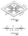
- Figs. 4A to 4C are views for explaining a first embodiment of the present invention, in which Fig. 4A is a perspective view showning an overall arrangement, Fig. 4B is a sectional view taken along a line IVB - IVB′ in Fig. 4A, and Fig. 4C is a sectional view taken along a line IVC - IVC′ in Fig. 4A.
- reference numerals 1A and 1B denote insulating flexible substrates.
- the substrates 1A and 1B are rectangular members having openings in their central portions.
- the substrates 1A and 1B may constitute a so-called ribbon-like structure in which substrates having the same structure are arranged side by side.
- Reference numeral 2 denotes an opening portion; 3, RF electrodes; 4, bias supply electrodes; 5, ground electrodes; 6, conductive leads; 8, element-side bumps; 8′, package-side bumps; 9, a bare-chip semiconductor element; 10, electrode pads; 11, a capillary; 12, a mounting substrate; 13, an electrode; 14, cut portions; and 15, a second opening portion formed in the insulating flexible substrate 1.
- an adhesive 7 is not used because it changes permittivity of the insulating flexible substrate 1, it can be similarly used as shown in Fig. 3B.
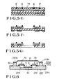
- a metal such as copper is deposited as underlying conductor films 51 on the front and rear surfaces of the insulating flexible substrate 1 consisting of a polyimide resin by sputtering, vapor deposition or the like.
- the thickness of the polyimide film is about 50 ⁇ m.
- it is effective to perform reverse sputtering of a small amount of Ar ions on the surfaces of the polyimide film before vapor deposition.
- a photoresist 52 is coated on both the surfaces, and the surfaces are exposed and developed to form an opening in a portion in which a waveguide conductor film is formed.
- a film-like resist e.g., LISTON (tradename) available from Du Pont de Nemours, E.I., Co. may be laminated on the flexible film.
- an etching mask conductor film 53 e.g., Ni is formed on the front side of the region opened by development. This film serves as a mask upon formation of an opening portion in the film.
- a waveguide conductor film 54 is formed on the surface by electrolytic plating.
- a second resist film 55 is formed, a necessary opening is formed, and then gold is deposited by electrolytic plating. Thereafter, as shown in Fig. 5F, the resist is removed.
- Fig. 5C an etching mask conductor film 53, e.g., Ni is formed on the front side of the region opened by development. This film serves as a mask upon formation of an opening portion in the film.
- a waveguide conductor film 54 is formed on the surface by electrolytic plating.
- a second resist film 55 is formed, a necessary opening is formed, and then gold is deposited by electrolytic plating. Thereafter, as shown in Fig. 5F, the resist is removed.
- Fig. 5C an etching mask conductor film 53,
- the polyimide film is etched by using the waveguide conductor film 54 and the etching mask conductor film 53 as masks to form an opening portion having a proper size in a predetermined portion.
- effective examples of an etchant are KOH and a solution mixture of ethanol and water.
- Fig. 4C is a sectional view showing a part of the coplanar waveguide of the film carrier.
- the waveguides are formed at four positions W1, W2, W3 and W4. That is, the outside waveguides W1 and W2 are coplanar waveguides formed to have a predetermined characteristic impedance by the central RF electrode 3, the ground electrodes 5 at both the sides of the RF electrode 3, and the insulating flexible substrate 1.
- the inside waveguides W3 and W4 are coplanar waveguides formed to have a predetermined characteristic impedance by the central RF electrode 3, the ground electrodes 5 at both the sides of the RF electrode 3, and the insulating flexible substrate 1.
- the waveguides W1 and W2 are connected to the waveguides W3 and W4, respectively, by the short leads 6.
- the short leads 6 projecting in the opening portion 2 are connected to the inside waveguides W3 and W4.
- the leads 6 are very short because the waveguides W3 and W4 are formed.
- the bias supply electrode 4 differs from the RF electrode 3.
- a part of the bias supply electrode 4 is used as the ground electrode 5 so that the bias supply electrode 4 is sandwiched by the ground electrodes 5, thereby constituting the coplanar waveguide structure. Therefore, it is apparent that the concept of the coplanar waveguide structure can be applied to the bias supply electrode 4. This will be the same in embodiments to be described later.
- Fig. 4D the waveguide film carrier is conveyed to a predetermined portion of the bare-chip semiconductor element 9 so that the element-side bumps 8 on the leads 6 overlap the electrode pads 10 formed on the bare-chip semiconductor 9.
- the leads 6 and the electrode pads 10 on the surface of the bare-chip semiconductor element 9 are heated and connected with each other by thermocompression bonding by using the capillary 11, thereby connecting and mounting the waveguide film carrier to the bare-chip semiconductor element 9.
- Fig. 4E is a partially-cutaway perspective view showing a connected/mounted state. In this state, RF characteristics of the bare-chip semiconductor can be measured. Mounting to packages of devices found to be defective as a result of the measurement is cancelled to improve the manufacturing yield of products.
- FIG. 4B A method of connecting and mounting the waveguide film carrier, on which the bare-chip semiconductor element 9 is connected and mounted, to a package will be described below.
- the leads 6 are cut at positions represented by reference numerals 14.
- the package-side bumps 8′ formed on the leads 6 overlap internal connection terminals 202. Therefore, the overlapped portions are heated by the capillary 11 and connected by thermocompression bonding.
- Fig. 6 is a sectional view showing an RF IC in which the bare-chip semiconductor and the film carrier are mounted in the package. Referring to Fig.
- reference numeral 201 denotes a package; 202, the internal connection terminals; 203, package input/output terminals; 60, a solder; and 70, a film carrier.
- the package 201 comprises a base portion 201a, a closed-loop or annular projecting portion 201b, a recess portion 201c formed in a central portion of the base portion 201a surrounded by the projecting portion 201b, and a conductor 201d formed across the projecting portion 201b on the base portion 201a and constituting the internal connection terminals 202 and the external connection terminals 203.
- the film carrier 70 mounting the bare-chip semiconductor element 9 thereon is dropped in a space surrounded by the projecting portion 201.
- the bare-chip semiconductor element 9 is housed in the recess portion 201c and fixed to the bottom of the recess portion 201c of the base 201a by the solder 60.
- the electrodes (3, 4 and 5 in Fig. 4A) of the carrier 70 are positioned on the internal connection terminals 202 of the package 201 and connected thereto directly or via the bumps.
- a seal ring 80 is placed on the projecting portion 201b and a metal cover 81 is placed thereon.
- These members are seam-joining to complete an RF IC.
- the connection point of the bare-chip semiconductor element 9 with respect to the film carrier 70 is preferably at the same level as that with respect to the internal connection terminals 202.
- the solder of the semiconductor element and the package also serves to equalize the levels. The solder may be replaced with an adhesive.
- a method of connecting and mounting the semiconductor element to a mounting substrate 12 will be described below.
- a first method as shown in Fig. 4F, the waveguide film carrier having the bare-chip semiconductor element 9 thereon is conveyed to a predetermined position on the mounting substrate 12, and the leads 6 and the electrode 13 on the surface of the mounting substrate 12 are heated by the capillary 11 and connected by thermocompression bonding, thereby connecting and mounting the waveguide film carrier on the mounting substrate 12. Thereafter, the rear surface of the bare-chip semiconductor element 9 is connected to the mounting substrate 12 by a solder or the like.
- the waveguide film carrier on which the bare-chip semiconductor element 9 is connected and mounted, is reversed so that an electrode surface of the bare-chip semiconductor element 9 serves as the electrode 13 surface of the mounting substrate 12.
- the waveguide film carrier is conveyed to a predetermined position on the mounting substrate 12, and the leads 6 and the electrode 13 of the surface of the mounting substrate 12 are heated by the capillary 11 and connected by thermocompression bonding, thereby connecting and mounting the waveguide film carrier on the mounting substrate 12.
- the substrate is cut at the cut portions 14 (Fig. 4D) formed in the second opening portion 15, and unnecessary leads 6 and an outer peripheral portion of the insulating flexible substrate 1A are disposed.
- the waveguide film carrier having the impedance-matched waveguides W3 and W4 is used for the connection between the bare-chip semiconductor element and the package or mounting substrate. Therefore, RF characteristics can be improved as compared with connections using wires, ribbons and the like.
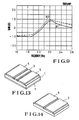
- Fig. 7 is a graph showing transmission characteristics of the coplanar waveguide of the above embodiment.
- the waveguide does not cause unnecessary resonance within a range of DC to 30 GHz and therefore can be applied to a wide-band circuit.
- Figs. 8 and 9 are the frequency characteristics of the MMIC (MMIC: monolythic microwave integrated circuit) amplifier chip comparing an RF characteristic curve 80 measured by connecting a meter directly to a bare-chip semiconductor with a characteristic curve 81 obtained by measuring a characteristic of the same element mounted in a package via the film carrier of the present invention from outside the package.
- Fig. 8 also shows a measured value 82 obtained when the element is mounted by using wires.
- MMIC monolythic microwave integrated circuit
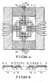
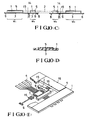
- Figs. 10A to 10D are views for explaining a second embodiment of the present invention, in which Fig. 10A is a plan view showing an arrangement of the second embodiment, Fig. 10B is a sectional view taken along a line XA - XA′ in Fig. 10A, Fig. 10C is a sectional view taken along a line XC - XC′ in Fig. 10A, and Fig. 10D is a sectional view taken along a line XD - XD′ in Fig. 10A.
- Ground electrodes 5 are formed on the surface opposite to RF electrodes 3 and are connected to leads 6 via through holes 16.
- Fig. 10E shows a state in which a bare-chip semiconductor 9 is mounted.
- a film carrier of the second embodiment is similar to that of the first embodiment in that all of the leads for connections are formed on one surface of an insulating substrate.
- a method of connecting the bare-chip semiconductor element 9 to the waveguide film carrier and a method of connecting the waveguide film carrier to a package or a mounting substrate 12 are the same as those in the first embodiment.
- Figs. 11A and 11B are views for explaining a third embodiment of the present invention.
- the third embodiment exemplifies a waveguide film carrier for connecting a plurality of bare-chip semiconductor elements.
- reference numeral 17 denotes a second bare-chip semiconductor element; 18, a third opening portion; and 19, a third bare-chip semiconductor element.
- a method of connecting and mounting the waveguide carrier to a package is similar to that in the first embodiment.
- a plurality of bare-chip semiconductor elements 9, 17 and 19 are connected by the waveguide film carrier having impedance-matched waveguides W1 to W5. Therefore, the RF characteristics can be improved as compared with those of connections using wires, ribbons and the like.
- the pattern of the waveguide film carrier can be easily changed by changing an etching mask, packages can be easily unified.
- Figs. 12A and 12B are views for explaining a fourth embodiment of the present invention.
- reference numerals 1 to 19 denote the same parts as in the embodiment shown in Figs. 11A and 11B.
- a plurality of bare-chip semiconductor elements 9, 17 and 19 are connected by a waveguide film carrier having impedance-matched waveguides W1 to W5. Therefore, the RF characteristics can be improved as compared with those obtained by connections using wires, ribbons and the like.
- the pattern of the waveguide film carrier can be easily changed, packages can be easily unified.
- Fig. 13 is a perspective view of a main part for explaining a fifth embodiment of the present invention.
- Fig. 13 shows a shielded coplanar waveguide as the waveguides W1 to W5 in each of the above embodiments.
- an RF electrode 3 is formed on the front surface of an insulating flexible substrate 1 and ground electrodes 5 are formed at both sides of the RF electrode 3, thereby constituting a coplanar waveguide.
- a ground electrode 5 having a shielding effect is formed on the rear surface of the insulating flexible substrate 1.
- the ground electrodes 5 on the front and rear surfaces are connected via through holes.
- Fig. 14 is a perspective view of a main part for explaining a sixth embodiment of the present invention.
- a pair of an RF electrode 3 and a ground electrode 5 are formed on one surface of an insulating flexible substrate 1.
- one or more opening portions are formed in a portion of an insulating flexible substrate, leads are formed in these opening portions, and RF, bias supply and ground electrodes are formed on or in the insulating flexible substrate, so that the RF and ground electrodes and the insulating flexible substrate constitute a waveguide having a predetermined characteristic impedance. Therefore, a lead length can be shortened, an inductance component of a lead can be reduced, and impedance match can be easily obtained. As a result, not only a bare-chip semiconductor element can be mounted while impedances are matched, but also a plurality of bare-chip semiconductor elements can be closely connected by using the insulating flexible substrate.
- a coplanar waveguide, a microstrip line, a shielded coplanar waveguide and a slot line can be selectively used as the waveguide in accordance with the number or the like of bare-chip semiconductor elements to be mounted.
Landscapes
- Wire Bonding (AREA)
Applications Claiming Priority (2)
| Application Number | Priority Date | Filing Date | Title |
|---|---|---|---|
| JP91593/88 | 1988-04-15 | ||
| JP9159388 | 1988-04-15 |
Publications (2)
| Publication Number | Publication Date |
|---|---|
| EP0337485A2 true EP0337485A2 (de) | 1989-10-18 |
| EP0337485A3 EP0337485A3 (de) | 1991-04-03 |
Family
ID=14030850
Family Applications (1)
| Application Number | Title | Priority Date | Filing Date |
|---|---|---|---|
| EP19890106727 Withdrawn EP0337485A3 (de) | 1988-04-15 | 1989-04-14 | Filmträger für integrierte RF-Schaltung |
Country Status (1)
| Country | Link |
|---|---|
| EP (1) | EP0337485A3 (de) |
Cited By (8)
| Publication number | Priority date | Publication date | Assignee | Title |
|---|---|---|---|---|
| EP0552701A3 (en) * | 1992-01-24 | 1993-09-01 | Sumitomo Electric Industries, Ltd. | Package for microwave device |
| EP0498446A3 (en) * | 1991-02-08 | 1993-10-20 | Toshiba Kk | Multichip packaged semiconductor device and method for manufacturing the same |
| EP0563969A3 (en) * | 1992-04-03 | 1993-10-27 | Mitsubishi Electric Corp | High frequency signal transmission tape and apparatus for bonding the high frequency signal transmission tape |
| EP0578028A1 (de) * | 1992-07-07 | 1994-01-12 | Mitsubishi Denki Kabushiki Kaisha | Hochfrequenz-Halbleiterbauelement |
| EP0540247A3 (en) * | 1991-10-28 | 1994-10-19 | Ibm | Formulation of multichip modules |
| EP0365783B1 (de) * | 1988-10-28 | 1995-02-01 | International Business Machines Corporation | Packungsstrukturen für integrierte Mehrschichtschaltungen |
| FR2747509A1 (fr) * | 1996-04-12 | 1997-10-17 | Nec Corp | Structure de montage pour un circuit a semi-conducteur |
| EP1174922A3 (de) * | 2000-07-18 | 2002-06-19 | Rosenberger Hochfrequenztechnik GmbH & Co. KG | Gehäuse für eine integrierte Schaltung mit Koplanarleitungen |
Family Cites Families (2)
| Publication number | Priority date | Publication date | Assignee | Title |
|---|---|---|---|---|
| US4543544A (en) * | 1984-01-04 | 1985-09-24 | Motorola, Inc. | LCC co-planar lead frame semiconductor IC package |
| EP0293838A3 (de) * | 1987-06-02 | 1989-09-06 | Kabushiki Kaisha Toshiba | Packung für integrierte Halbeiterschaltungsanordnung hoher Geschwindigkeit |
-
1989
- 1989-04-14 EP EP19890106727 patent/EP0337485A3/de not_active Withdrawn
Cited By (11)
| Publication number | Priority date | Publication date | Assignee | Title |
|---|---|---|---|---|
| EP0365783B1 (de) * | 1988-10-28 | 1995-02-01 | International Business Machines Corporation | Packungsstrukturen für integrierte Mehrschichtschaltungen |
| EP0498446A3 (en) * | 1991-02-08 | 1993-10-20 | Toshiba Kk | Multichip packaged semiconductor device and method for manufacturing the same |
| EP0540247A3 (en) * | 1991-10-28 | 1994-10-19 | Ibm | Formulation of multichip modules |
| EP0552701A3 (en) * | 1992-01-24 | 1993-09-01 | Sumitomo Electric Industries, Ltd. | Package for microwave device |
| US5416660A (en) * | 1992-01-24 | 1995-05-16 | Sumitomo Electric Industries, Ltd. | Package for microwave device |
| EP0563969A3 (en) * | 1992-04-03 | 1993-10-27 | Mitsubishi Electric Corp | High frequency signal transmission tape and apparatus for bonding the high frequency signal transmission tape |
| US5349317A (en) * | 1992-04-03 | 1994-09-20 | Mitsubishi Denki Kabushiki Kaisha | High frequency signal transmission tape |
| EP0578028A1 (de) * | 1992-07-07 | 1994-01-12 | Mitsubishi Denki Kabushiki Kaisha | Hochfrequenz-Halbleiterbauelement |
| US5426319A (en) * | 1992-07-07 | 1995-06-20 | Mitsubishi Denki Kabushiki Kaisha | High-frequency semiconductor device including microstrip transmission line |
| FR2747509A1 (fr) * | 1996-04-12 | 1997-10-17 | Nec Corp | Structure de montage pour un circuit a semi-conducteur |
| EP1174922A3 (de) * | 2000-07-18 | 2002-06-19 | Rosenberger Hochfrequenztechnik GmbH & Co. KG | Gehäuse für eine integrierte Schaltung mit Koplanarleitungen |
Also Published As
| Publication number | Publication date |
|---|---|
| EP0337485A3 (de) | 1991-04-03 |
Similar Documents
| Publication | Publication Date | Title |
|---|---|---|
| US5294897A (en) | Microwave IC package | |
| KR100541580B1 (ko) | 반도체 장치 및 그 제조 방법 | |
| US5182631A (en) | Film carrier for RF IC | |
| US4991001A (en) | IC packing device with impedance adjusting insulative layer | |
| US6175241B1 (en) | Test carrier with decoupling capacitors for testing semiconductor components | |
| EP0457985A1 (de) | Mikrowellenhalbleiteranordnung | |
| US5495125A (en) | Molded semiconductor device | |
| JPH04137655A (ja) | Icパッケージ | |
| EP1520296B1 (de) | Tragbarer silizium chip | |
| US5426319A (en) | High-frequency semiconductor device including microstrip transmission line | |
| EP0337485A2 (de) | Filmträger für integrierte RF-Schaltung | |
| US20030222342A1 (en) | Multi-chip package | |
| US5532906A (en) | Wiring substrate | |
| KR100270954B1 (ko) | 갈륨 아세나이드 집적회로 용 와이어본딩되지 않은 입/출력 인터페이스 | |
| JPS61114562A (ja) | マイクロ波用チツプキヤリヤ | |
| JP3058898B2 (ja) | 半導体装置及びその評価方法 | |
| EP0293838A2 (de) | Packung für integrierte Halbeiterschaltungsanordnung hoher Geschwindigkeit | |
| EP1267459A1 (de) | Kühlkörper für Laser im Elektronikgehäuse | |
| JP2666156B2 (ja) | 高周波ic用フイルムキヤリア | |
| JP4127589B2 (ja) | 高周波半導体装置用パッケージおよび高周波半導体装置 | |
| GB2292833A (en) | Microwave integrated circuit and method of fabrication | |
| JP3112253B2 (ja) | 高周波用半導体装置 | |
| JP2000164970A (ja) | 光素子モジュール | |
| JP2532126B2 (ja) | 導波路形フィルムキャリアおよびその端子接続方法 | |
| JP3170017B2 (ja) | 半導体装置 |
Legal Events
| Date | Code | Title | Description |
|---|---|---|---|
| PUAI | Public reference made under article 153(3) epc to a published international application that has entered the european phase |
Free format text: ORIGINAL CODE: 0009012 |
|
| 17P | Request for examination filed |
Effective date: 19890509 |
|
| AK | Designated contracting states |
Kind code of ref document: A2 Designated state(s): DE FR GB SE |
|
| PUAL | Search report despatched |
Free format text: ORIGINAL CODE: 0009013 |
|
| AK | Designated contracting states |
Kind code of ref document: A3 Designated state(s): DE FR GB SE |
|
| 17Q | First examination report despatched |
Effective date: 19930217 |
|
| RAP1 | Party data changed (applicant data changed or rights of an application transferred) |
Owner name: NIPPON TELEGRAPH AND TELEPHONE CORPORATION |
|
| STAA | Information on the status of an ep patent application or granted ep patent |
Free format text: STATUS: THE APPLICATION IS DEEMED TO BE WITHDRAWN |
|
| 18D | Application deemed to be withdrawn |
Effective date: 19960626 |